Microcomputer Circuits and Processes
Microcomputer Circuits and Processes
Microcomputer Circuits and Processes

Create successful ePaper yourself
Turn your PDF publications into a flip-book with our unique Google optimized e-Paper software.
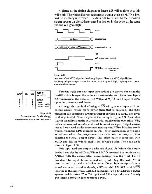
A glance at the timing diagram in figure 2.28 will confirm that this<br />
will work. The whole diagram refers to an output cycle, so M/IO is low,<br />
<strong>and</strong> no memory is involved. The data bits to be sent to the television<br />
screen appear on the address-data bus late on in the cycle, at the same<br />
time as WR goes high.<br />
clock<br />
=x"'"-- a_d_d_re_ss >c address bus<br />
=x address X data to TV screen >c. address-data bus<br />
JI'---<br />
RD<br />
L-- WR high means<br />
_<br />
ALE<br />
output<br />
--, I MjTO low, i.e. input-output<br />
1-1 ----', operation<br />
Figure 2.28<br />
Addition of the MilO signal to the timing diagram. Here, the MilO signal is low,<br />
implying an input-output instruction. Also, the WR signal is high, implying a write, here<br />
an output instruction.<br />
M/ra RD WR<br />
type of<br />
operation<br />
0 0<br />
,<br />
output<br />
0 1 0 input<br />
0<br />
,<br />
memory write<br />
, , 0 memory read<br />
Figure 2.29<br />
Operation types for the allowed<br />
combinations ofRD, WR, <strong>and</strong> MilO.<br />
You can work out how input instructions are carried out using the<br />
read (RD) line to open the buffer on the input device. The table in figure<br />
2.29 summarizes the states of RD, WR, <strong>and</strong> M/IO for all types of CPU<br />
operation, memory <strong>and</strong> in-out.<br />
Although thiJ method of using M/IO will give one input <strong>and</strong> one<br />
output device, rather more power than that is required. The 8086<br />
processor can control 64000 input/output devices! The M/IO line gives<br />
us that potential. Glance again at the timing in figure 2.28. Note that<br />
there is an address on the address bus during the entire operation. Why<br />
is this address not decoded <strong>and</strong> used to select an input-output device,<br />
just as it was used earlier to select a memory card? That is in fact how it<br />
works. When the CPU executes an OUT or IN instruction, it will send<br />
an address which the programmer can write into the program, thus<br />
selecting the input-output device. This select pulse is combined with<br />
M/IO <strong>and</strong> RD or WR to enable the device's buffer. The hook-up is<br />
shown in figure 2.30.<br />
One input <strong>and</strong> one output device are shown. As before, the output<br />
device is enabled by ANDing WR <strong>and</strong> M/IO inverted, but now it is also<br />
ANDed with the device select signal coming from the 4-bit, 1-of-16<br />
decoder. The input device is enabled by ANDing RD with M/IO<br />
inverted <strong>and</strong> the device selection pulse. Other input-output devices<br />
would use other selection signals, ANDing with RD, WR, <strong>and</strong> M/IO<br />
inverted in the same way. With full decoding of an 8-bit address bus, the<br />
system could control 2 8 = 256 input <strong>and</strong> 256 output devices. Already<br />
our simple computer has enormous power.<br />
24