- Page 1: OSBORNE 16-Bit Microprocessor Handb
- Page 4 and 5: Copyright © 1981, 1979, 1978, 1976
- Page 7 and 8: Contents 1. The National Semiconduc
- Page 9 and 10: INTRODUCTION This is one o'f two bo
- Page 11 and 12: Thus a signal making a low-to-high
- Page 13: We will demonstrate the capriciousn
- Page 16 and 17: Before making direct comparisons of
- Page 18 and 19: SENSE LINES IN INS8900 TWO INS8208s
- Page 20 and 21: INS8900 AND PACE ADDRESSING MODES M
- Page 22 and 23: This illustration shows base page.
- Page 24 and 25: INS8900 AND PACE CPU PINS AND SIGNA
- Page 26 and 27: The INSS900 clock logic has been si
- Page 28 and 29: The maximum extension permitted by
- Page 30 and 31: ....I ....I ~ EXECUTION ..... f----
- Page 32 and 33: There are two draw\Jacks inherent i
- Page 34 and 35: IRO INT ENABLE lEN NHALT LEVEL 0 IN
- Page 36 and 37: The interrupt sequence does not sav
- Page 38 and 39: ecute a Jump Indirect (JMP@) throug
- Page 40 and 41: The following symbols are used in T
- Page 42 and 43: Table 1-1. INS8900 and PACE Instruc
- Page 44 and 45: Table 1-1. INS8900 and PACE Instruc
- Page 46 and 47: Table 1-2. INS8900 and PACE Instruc
- Page 48 and 49: Memory, as organized for the benchm
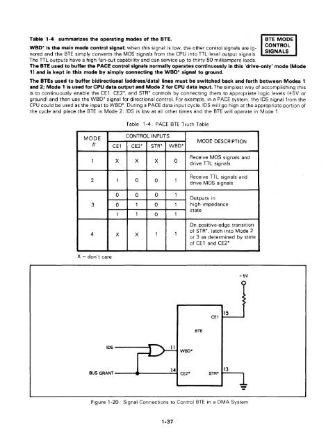
- Page 52 and 53: In a DMA or multiprocessor we will
- Page 54 and 55: Notice that the data from external
- Page 56 and 57: When the output port's address is s
- Page 58 and 59: One other portion of Table 1-5 requ
- Page 60 and 61: PACE CPU r - -;;,;;;.;---- - - - ;;
- Page 62 and 63: PACE CPU EXTRA CLOCK CYCLEISIOUE IN
- Page 64 and 65: INS8900 Absolute Maximwn Ratings Vo
- Page 66 and 67: INS8900 Tming Waveforms ~ J ttl- jJ
- Page 68 and 69: INS8900 Tming Wavefonns (continued)
- Page 70 and 71: PACE STE absolute maximum ratings [
- Page 72 and 73: PACE BTE/S absolute maximum ratings
- Page 74 and 75: PACE STE/S switching' time waveform
- Page 77 and 78: Chapter 2 THE GENERAL INSTRUMENT CP
- Page 79 and 80: CP1600 PROGRAMMABLE REGISTERS The C
- Page 81 and 82: If Register R4 or R5 provides the i
- Page 83 and 84: ESCI MSYNc' BCl BC2 BDIR 015 014 01
- Page 85 and 86: MC MC T1 T2 T3 T4 T1 T2 T3 T4 BC 1
- Page 87 and 88: INSTRUCTION FETCH MEMORY WRITE BAR
- Page 89 and 90: The PerF signal as an input inhibit
- Page 91 and 92: INSTRUCTION FETCH INSTRUCTION EXECU
- Page 93 and 94: SW The Status Word. whose bits corr
- Page 95 and 96: I Table 2-2. CP1600 Instruction Set
- Page 97 and 98: Table 2-2. CP1600 Instruction Set S
- Page 99 and 100: Table 2-3. CP1600 Branch Conditions
- Page 101 and 102:
Table 2-4. CP1600 Instruction Set O
- Page 103 and 104:
SUPPORT DEVICES THAT MAY BE USED WI
- Page 105 and 106:
=rt-01~~1 .. DATA READ ..J ,I II I
- Page 107 and 108:
Interrupts may be generated by cond
- Page 109 and 110:
Bit 0 is always the complement of t
- Page 111 and 112:
When the CPU is ready to receive da
- Page 113 and 114:
The only accurate long time interva
- Page 115 and 116:
DATA SHEETS This section contains s
- Page 117 and 118:
CP1600 ELECTRICAL CHARACTERISTICS (
- Page 119 and 120:
CP1610 ELECTRICAL CHARACTERISTICS (
- Page 121 and 122:
Chapter 3 THE TEXAS INSTRUMENTS TMS
- Page 123 and 124:
Let us first consider the manner in
- Page 125 and 126:
can begin executing a new program.
- Page 127 and 128:
efore you switched to your current
- Page 129 and 130:
A CRU bit instruction outputs a 12-
- Page 131 and 132:
When bits are transferred from a me
- Page 133 and 134:
or the high-order byte of a general
- Page 135 and 136:
Pins AO - A 14 provide the 15-bit A
- Page 137 and 138:
DBIN goes high at the beginning of
- Page 139 and 140:
If the second (destination) operand
- Page 141 and 142:
Every CRU 1/0 instruction will requ
- Page 143 and 144:
The Address Bus is used in an unusu
- Page 145 and 146:
THE HOLD STATE The TMS 9900 has a t
- Page 147 and 148:
External logic identifies the prior
- Page 149 and 150:
At the conclusion of the interrupt
- Page 151 and 152:
decoder is high, the four outputs,
- Page 153 and 154:
A14 A13 A12 A11 AD 'M"EMEN CRUOUT C
- Page 155 and 156:
The CPU checks LOAD at the end of e
- Page 157 and 158:
The following symbols are used in T
- Page 159 and 160:
Table 3-2. TMS 9900 Instruction Set
- Page 161 and 162:
Table 3-2. TMS 9900 Instruction Set
- Page 163 and 164:
Table 3-3. TMS 9900 Instruction Set
- Page 165 and 166:
Figure 3-14 illustrates that part o
- Page 167 and 168:
HOLD HLDA IAQ (LSB) (AO) CRUOUT/A13
- Page 169 and 170:
TMS 9980 SERIES MICROPROCESSOR TIMI
- Page 171 and 172:
Memory Address Reset ~ ~ Memory Byt
- Page 173 and 174:
• Two levels of external interrup
- Page 175 and 176:
The TMS 9940 does introduce one add
- Page 177 and 178:
The TMS 9940-can, in fact. use stan
- Page 179 and 180:
Table 3-7 shows how the TMS 9940 in
- Page 181 and 182:
2) The address output on A 1 1- A8
- Page 183 and 184:
You could use the CRU to perform an
- Page 185 and 186:
TMS 9940 GENERAL PURPOSE FLAGS If y
- Page 187 and 188:
2) The XOP instructions will not wo
- Page 189 and 190:
When an external quartz crystal is
- Page 191 and 192:
Clock Logic Arithmetic and Logic Un
- Page 193 and 194:
.~ TMS 9901 PSI PINS AND SIGNALS Th
- Page 195 and 196:
ICO ~--.r---, INTERRUPT MASK BITS o
- Page 197 and 198:
You access interrupt logic through
- Page 199 and 200:
generate data in two CRU bits, one
- Page 201 and 202:
Either of the following two events
- Page 203 and 204:
Table 3-9, 'TMS9902 Control and Sta
- Page 205 and 206:
3) Write to the Interval Timer regi
- Page 207 and 208:
When the break control bit is set t
- Page 209 and 210:
The time interval separating serial
- Page 211 and 212:
Transmit logic has now been initial
- Page 213 and 214:
TMS9902 RECEIVE OPERATIONS As soon
- Page 215 and 216:
THE TMS9903 SYNCHRONOUS COMMUNICATI
- Page 217 and 218:
We will describe programming aspect
- Page 219 and 220:
Table 3-12. TMS9903 Synchronous Com
- Page 221 and 222:
Note carefully that in SDLC mode yo
- Page 223 and 224:
We will next describe the Parameter
- Page 225 and 226:
In Monosync mode a single Sync char
- Page 227 and 228:
Table 3-14. TMS9903 Synchronous Com
- Page 229 and 230:
TMS9903 INTERRUPT LOGIC There are s
- Page 231 and 232:
for the short frame may go undetect
- Page 233 and 234:
DATA SHEE"rS The following pages co
- Page 235 and 236:
TMS9900 TIMING REQUIREMENTS OVER FU
- Page 237 and 238:
TMS9940 RECOMMENDED PROGRAMMINGITES
- Page 239 and 240:
TMS9940 CLOCK CHARACTERISTICS Inter
- Page 241 and 242:
TIM9904 Switching Characteristics,
- Page 243 and 244:
TMS9901 Electrical Characteristics
- Page 245 and 246:
TMS9902 TMS 9902 ELECTRICAL SPECIFI
- Page 247 and 248:
TMS9903 EQUIVALENT OF OUTPUTS EQUIV
- Page 249:
TMS9903 nMING REQUIREMENTS OVER FUL
- Page 252 and 253:
Using a 240 nanosecond clock. the M
- Page 254 and 255:
There is one further major differen
- Page 256 and 257:
placement is treated as a signed bi
- Page 258 and 259:
Indirect. indexed addressing may be
- Page 260 and 261:
NOVA STATUS FLAGS Nova minicomputer
- Page 262 and 263:
The Memory Bus consists of a 16-bit
- Page 264 and 265:
C3 1 40 MO C2 2 39 M1 C1 3 38 M2 CO
- Page 266 and 267:
The following sequence is sufficien
- Page 268 and 269:
CPU LOGIC AND INSTRUCTION EXECUTION
- Page 270 and 271:
The numbers CD . ® . (3) . 0 and (
- Page 272 and 273:
This is how the Busy and Done statu
- Page 274 and 275:
__ __ ___ ______ __________ These a
- Page 276 and 277:
MBUSY is a signal used by external
- Page 278 and 279:
An actual example of I/O device log
- Page 280 and 281:
MICRONOVA AND 9440 INTERRUPT PROCES
- Page 282 and 283:
acknowledge signal output by the Mi
- Page 284 and 285:
If you want to nest interrupts then
- Page 286 and 287:
The following notation is used in T
- Page 288 and 289:
Table 4-2. MicroNova and 9440 Instr
- Page 290 and 291:
Table 4-2. MicroNova and 9440 Instr
- Page 292 and 293:
Table 4-2. MicroNova and 9440 Instr
- Page 294 and 295:
tt www xx Two bits choosing the I/O
- Page 296 and 297:
() +5V '--- 0 -- ~CK I PRE LS74 ~ Q
- Page 298 and 299:
This timing is also illustrated in
- Page 300 and 301:
iBO iBi SELB SELD YO iR'5 C Yi iR6
- Page 302 and 303:
The LS 139 2-to-4 decoder decodes i
- Page 304 and 305:
y MEMORY CLOCK. In order that all w
- Page 307 and 308:
DATA SHEETS This section contains s
- Page 309 and 310:
MICRONOVA D. C. (STATIC) CHARACTERI
- Page 311 and 312:
9440 AC CHARACTERISTICS: T A = 0 to
- Page 313 and 314:
9440 AC CHARACTERISTICS: TA = 0 to
- Page 315 and 316:
9440 AC CHARACTERISTICS: TA = 0 to
- Page 317 and 318:
Chapter 5 THE INTEL 8086 The 8086 i
- Page 319 and 320:
The 8086 has a large family of supp
- Page 321 and 322:
8086 PROGRAMMABLE REGISTERS AND ADD
- Page 323 and 324:
All 8086 memory addresses are compu
- Page 325 and 326:
Any Stack instruction such as a Pus
- Page 327 and 328:
Instructions that access data memor
- Page 329 and 330:
Let us now examine the various data
- Page 331 and 332:
We may now illustrate direct, index
- Page 333 and 334:
Base relative implied data memory a
- Page 335 and 336:
The 8086 also has Stack memory addr
- Page 337 and 338:
Here is an illustration of base rel
- Page 339 and 340:
8086 CPU PINS AND SIGNALS 8086 CPU
- Page 341 and 342:
In the previous illustration you wi
- Page 343 and 344:
RD is a single bus control signal t
- Page 345 and 346:
The eight combinations of 52. 51. a
- Page 347 and 348:
If memory or an I/O device must be
- Page 349 and 350:
But the 8086. having asynchronous C
- Page 351 and 352:
Note that the CPU may have to wait
- Page 353 and 354:
For an 8286 or 8287 Bus Transceiver
- Page 355 and 356:
The 8288 Bus Controller. described
- Page 357 and 358:
If there is an active Hold request
- Page 359 and 360:
If a 16-bit data word lies on an od
- Page 361 and 362:
A number of the Vector table entrie
- Page 363 and 364:
SINGLE STEPPING MODE When the T sta
- Page 365 and 366:
Secondary memory reference instruct
- Page 367 and 368:
AAS instruction operations may be s
- Page 369 and 370:
Table 5-2. 8086 Branch-an-Condition
- Page 371 and 372:
The LOCK must directly precede MOVS
- Page 373 and 374:
The following abbreviations are use
- Page 375 and 376:
sss PPOO v x yy yyyy represents thr
- Page 377 and 378:
Table 5-4. A Summary of 8086 and 80
- Page 379 and 380:
Table 5-4. A Summary of 8086 and 80
- Page 381 and 382:
Table 5-4. A Summary of 8086 and 80
- Page 383 and 384:
I Table 5-4. A Summary of 8086 and
- Page 385 and 386:
Table 5-4. A Summary of 8086 and 80
- Page 387 and 388:
Table 5-4. A Summary of 8086 and 80
- Page 389 and 390:
! Table 5-4. A Summary of 8086 and
- Page 391 and 392:
Table 5-4. A Summary of 8086 and 80
- Page 393 and 394:
Table 5-4. A Summary of 8086 and 80
- Page 395 and 396:
Table 5-4. A Summary of 8086 and 80
- Page 397 and 398:
i I Table 5-4. A Summary of 8086 an
- Page 399 and 400:
Table 5-5. 8086 and 8088 Instructio
- Page 401 and 402:
Table 5-5. 8086 and 8088 Instructio
- Page 403 and 404:
Table 5-5. 8086 and 8088 Instructio
- Page 405 and 406:
Table 5-6. 8086 and 8088 Instructio
- Page 407 and 408:
Table 5-6. 8086 and 8088 Instructio
- Page 409 and 410:
Table 5-6. 8086 and 8088 Instructio
- Page 411 and 412:
Table 5-7. 8080A to 8086 Instructio
- Page 413 and 414:
THE 8088 CPU The 8088 is an 8086 mi
- Page 415 and 416:
8088 TIMING AND INSTRUCTION EXECUTI
- Page 417 and 418:
THE INTEL 8284 CLOCK GENERATOR/DRIV
- Page 419 and 420:
CSYNC PCLK AEN1 RDY1 READY RDY2 AEN
- Page 421 and 422:
In multi-CPU configurations you wil
- Page 423 and 424:
THE INTEL 8288 BUS CONTROLLER In co
- Page 425 and 426:
8288 and 8086 control signal timing
- Page 427 and 428:
THE 8282/8283 8-BIT INPUT/OUTPUT LA
- Page 429 and 430:
AO A1 A2 A3 A4 A5 A6 A7 OE GND -- -
- Page 431 and 432:
ALE - ~ +DE ADO ~ - \ r AD7 8282 ST
- Page 433 and 434:
DATA SHEETS This section contains s
- Page 435 and 436:
8086/8086-2/8086-4 A.C. CHARACTERIS
- Page 437 and 438:
8086/8086-2/8086-4 CLK (8284 Oulpul
- Page 439 and 440:
8086/8086-2/8086-4 OSo,OS, !i.II.SO
- Page 441 and 442:
8086/8086-2/8086-4 CL'~ I I L TINYC
- Page 443 and 444:
8088 A.C. CHARACTERISTICS 8088: TA=
- Page 445 and 446:
8088 ClK (828~ Output) I WRITE ~~~~
- Page 447 and 448:
8088 T, T, ClK VCl OSo.OS, S"S"So (
- Page 449 and 450:
8088 NOTE: 1. SETUP REQUIREMENTS FO
- Page 451 and 452:
8282/8283 INPUTS 1= )K '" ' r~'==tm
- Page 453 and 454:
8284 ABSOLUTE MAXIMUM RATINGS· Tem
- Page 455 and 456:
8286/8287 ABSOLUTE MAXIMUM RATINGS
- Page 457 and 458:
8286/8287 50 50 8217 40 40 u III 30
- Page 459 and 460:
8288 STATE eLK ADDRESS/DATA ALE ) )
- Page 461 and 462:
Chapter 6 THE ZILOG Z8000 SERIES Th
- Page 463 and 464:
THE Z8001 AND Z8002 CPU'S Because t
- Page 465 and 466:
15 14 13 12 11 10 9 8 7 6 5 4 3 2 o
- Page 467 and 468:
The Parity, Overflow, Sign, Zero, a
- Page 469 and 470:
Z8000 REGISTER DESIGNATIONS Z8000 s
- Page 471 and 472:
The index or displacement portion o
- Page 473 and 474:
A Za001 direct memory address may b
- Page 475 and 476:
Long segmented Z8001 indexed addres
- Page 477 and 478:
Long segmented base relative addres
- Page 479 and 480:
AD9 AD10 AD11 AD12 AD13 STOP Mi AD1
- Page 481 and 482:
When a zaooo microprocessor execute
- Page 483 and 484:
Z8001 AND Z8002 TIMING AND INSTRUCT
- Page 485 and 486:
14----T1---_.I ..... r-----T2---...
- Page 487 and 488:
I--T1--1 .... • --T2--"-1---TW --
- Page 489 and 490:
I: Memory Refresh T1 -\- T2 -I· T3
- Page 491 and 492:
Last machine cycle Instruction fetc
- Page 493 and 494:
Last machine cycle Aborted Instruct
- Page 495 and 496:
The segmentation trap. internal sof
- Page 497 and 498:
Block transfer instructions may tra
- Page 499 and 500:
The multiply instruction also has w
- Page 501 and 502:
As illustrated above. the contents
- Page 503 and 504:
THE BENCHMARK PROGRAM The Z8000 can
- Page 505 and 506:
Object Code b - immediate value cor
- Page 507 and 508:
Table 6-3. A Summary of the Z8000 I
- Page 509 and 510:
Table 6-3. A Summary of the Z8000 I
- Page 511 and 512:
I I I i Table 6-3. A Summary of the
- Page 513 and 514:
Table G-3. A Summary of the Z8000 I
- Page 515 and 516:
Table 6-3. A Summary of the Z8000 I
- Page 517 and 518:
Table 6-3. A Summary of the zaooo I
- Page 519 and 520:
Table 6-3. A Summary of the Z8000 I
- Page 521 and 522:
Table 6-3. A Summary of the Z8000 I
- Page 523 and 524:
Table 6-3. A Summary of the Z8000 I
- Page 525 and 526:
Table 6-3. A Summary of the Z8000 I
- Page 527 and 528:
0) m ..,J Table 6-3. A Summary of t
- Page 529 and 530:
Copyright © 1 979 McGraw-Hili, Inc
- Page 531 and 532:
Table 6-3. A Summary of the Z8000 I
- Page 533 and 534:
Table 6-3. A Summary of the Z8000 I
- Page 535 and 536:
Mnemonic Object Code Bytes Table 6-
- Page 537 and 538:
Table 6-4. Z8000 Instruction Set Ob
- Page 539 and 540:
Table 6-4. Z8000 Instruction Set Ob
- Page 541 and 542:
Table 6-4. Z8000 Instruction Set Ob
- Page 543 and 544:
Table 6-5. Z8000 Object Codes (Cont
- Page 545:
Table 6-5. Z8000 Object Codes (Cont
- Page 548 and 549:
Z8001,Z8002 Composite AC Timing Dia
- Page 550 and 551:
Z8001,Z8002 Absolute Maximum Rating
- Page 552 and 553:
The primary source for the MC68000
- Page 554 and 555:
As we have already pointed out. all
- Page 556 and 557:
System Byte ~~--.... --~~~------~,
- Page 558 and 559:
04 03 02 01 DO AS UDS LOS R/W OTACK
- Page 560 and 561:
A1-A23~ __________ ________________
- Page 562 and 563:
I 50 I 51 I 52 I 53 I 54 55 I 56 I
- Page 564 and 565:
ClK A1-A23---{~ ______________ ~~~
- Page 566 and 567:
elK A1-A23 R/W 00-015 -----..... Fi
- Page 568 and 569:
Figure 7-11 illustrates the timing
- Page 570 and 571:
Completion of Halt State. Address B
- Page 572 and 573:
Figure 7-13 shows the successful co
- Page 574 and 575:
The MC68000 provides extensive exce
- Page 576 and 577:
Memory Addresses 1---16 Bits (Hex
- Page 578 and 579:
---------j 0 = Write cycle aborted
- Page 580 and 581:
7) The contents of the Status regis
- Page 582 and 583:
Register Direct Addressing This add
- Page 584 and 585:
Address Registers AO ~-------------
- Page 586 and 587:
Address Registers AO~ _____________
- Page 588 and 589:
Byte .,___ o_o_o_o_o_oo_o ____ ~ __
- Page 590 and 591:
ABBREVIA TIONS Following are the ab
- Page 592 and 593:
STATUS The effect of instruction ex
- Page 594 and 595:
eeeee [EXT] ffffff gggggg hhhhhh ii
- Page 596 and 597:
Standard Read Cycle .. I. 6800 Peri
- Page 598 and 599:
+5 V o AS~----~--4~;---------------
- Page 600 and 601:
Table 7-5. MC68000 Instructions Whi
- Page 602 and 603:
Table 7-6. MC68000 Instruction Set
- Page 604 and 605:
I I I I I I Table 1-6 .. MC68000 In
- Page 606 and 607:
Table 7-6. MC68000 Instruction Set
- Page 608 and 609:
Table 7-6. MC68000 Instruction Set
- Page 610 and 611:
I Table 7-6. MC68000 Instruction Se
- Page 612 and 613:
Table 7-6. MC68000 Instruction Set
- Page 614 and 615:
Table 7-6. MC68000 Instruction Set
- Page 616 and 617:
I Table 7-6. MC68000 Instruction Se
- Page 618 and 619:
Table 7-6. MC68000 Instruction Set
- Page 620 and 621:
Table 7-6. MC68000 Instruction Set
- Page 622 and 623:
I Table 7-6. MC68000 Instructim Set
- Page 624 and 625:
Table 7-6. MC68000 Instruction Set
- Page 626 and 627:
Table 7-7. MC68000 Instruction Obje
- Page 628 and 629:
Table 7-7. MC68000 Instruction Obje
- Page 630 and 631:
Table 7-7. MC6SOOO Instruction Obje
- Page 632 and 633:
Table 7-7. MC68000 Instruction Obje
- Page 634 and 635:
Table 7-8. MC68000 Object Codes in
- Page 636:
Table 7-8. MC68000 Object Codes in
- Page 642 and 643:
THE 2901, 2901 A, AND 2901 B MICROP
- Page 644 and 645:
THE 2901, 2901A, AND 29018 MICROPRO
- Page 646 and 647:
,....----,1>-........ 0 RAM3 CL~~D-
- Page 648 and 649:
00-03 is a data input port. All dat
- Page 650 and 651:
The 2901 local RAM consists of sixt
- Page 652 and 653:
The 2901 local RAM generates a 4-bi
- Page 654 and 655:
The Q register is a single 4-bit lo
- Page 656 and 657:
Table 8-1. ALU Source Operand Contr
- Page 658 and 659:
~ .- "% 3-IN MUX t 3-IN MUX I Local
- Page 660 and 661:
" ","',"",·',w. ",,",'. I, t ,', "
- Page 662 and 663:
, ~ ,'" , t: , ,,",',' ~Z.'~UX $fif
- Page 664 and 665:
Local RAM Q Register A Latch B Latc
- Page 666 and 667:
Let us now examine status logic of
- Page 668 and 669:
CD ~ CJ) i7 yy I sr r 1 T 1 1 1 T 1
- Page 670 and 671:
Given the bit numbering system used
- Page 672 and 673:
17 SO 51 !±b 1G A B 2G 17 50 51 !
- Page 674 and 675:
An arithmetic upshift causes 0 to b
- Page 676 and 677:
We described logic associated with
- Page 678 and 679:
This is the algorithm we are about
- Page 680 and 681:
In Figure 8-15. CX and CY high is t
- Page 682 and 683:
THE 2903 MICROPROCESSOR SLICE The 2
- Page 684 and 685:
AO A Word A1 Address A2 { A3 16 x 4
- Page 686 and 687:
2903 MICROPROCESSOR SLICE PINS AND
- Page 688 and 689:
At intermediate and most significan
- Page 690 and 691:
The A latch contents are output con
- Page 692 and 693:
Beginning with the logically simple
- Page 694 and 695:
Now consider the data paths we just
- Page 696 and 697:
We can take the S ALU input from DB
- Page 698 and 699:
The 2903 has local RAM addressing.
- Page 700 and 701:
Table 8-7. 2903 Destination and Shi
- Page 702 and 703:
The ALU shifter, but not the Q shif
- Page 704 and 705:
By holding WE high you can output d
- Page 706 and 707:
You can use this pair of ALU destin
- Page 708 and 709:
Table 8-8. 2903 Special Functions S
- Page 710 and 711:
There are some differences between
- Page 712 and 713:
Z = FO • Pi . . . FN • QO • Q
- Page 714 and 715:
The negative status, N, is output h
- Page 716 and 717:
multiplier is in the low-order bit
- Page 718 and 719:
+5V () - 00, L5S .... 0103 0100 010
- Page 720 and 721:
But what happens if you get a negat
- Page 722 and 723:
Move the divisor and most significa
- Page 724 and 725:
If you look again at Table 8-9, you
- Page 726 and 727:
For Step 1 we execute the Double Le
- Page 728 and 729:
Finally. in Step 4 we execute a Two
- Page 730 and 731:
DO - 03 04 - 07" 08 - 011 012 - 015
- Page 732 and 733:
CIN 2901's r ----------------------
- Page 734 and 735:
THE 2909 AND 2911 MICROPROGRAM SEQU
- Page 736 and 737:
Macroinstruction object codes have
- Page 738 and 739:
RE R3 R2 R1 RO OR3 03 OR2 02 OR1 01
- Page 740 and 741:
RE ------------------~ Stack Po.int
- Page 742 and 743:
Microprogram Counter will be one mo
- Page 744 and 745:
Consider first a typical subroutine
- Page 746 and 747:
Table 8-11. The 2903 Twos Complemen
- Page 748 and 749:
Status outputs from the 2901 or 290
- Page 750 and 751:
Address Bits from Status from Micro
- Page 752 and 753:
THE 2910 MICROPROGRAM SEQUENCER Thi
- Page 754 and 755:
DO-Dll&~~ ~ Address Register/ ~ Dow
- Page 756 and 757:
DO - 011. 10 -13 Control Inputs 1--
- Page 758 and 759:
Table 8-12. 2910 Microprogram Seque
- Page 760 and 761:
When the 2910 receives an RFCT inst
- Page 762 and 763:
2910 MICROPROGRAM SEQUENCER ADDRESS
- Page 764 and 765:
Table 8-13. The 2903 Twos Complemen
- Page 766 and 767:
egister. As we did in instruction 2
- Page 768 and 769:
10 EMPTY CI OE C(I+4) CN YO Y1 Y2 Y
- Page 770 and 771:
Table 8-14. 2930 Series Program Con
- Page 773 and 774:
DATA SHEETS This section contains s
- Page 775 and 776:
Am2901 /2901 A SOURCE OPERANDS AND
- Page 777 and 778:
Am2901 ELECTRICAL CHARACTERISTICS O
- Page 779 and 780:
Am2901A ELECTRICAL CHARACTERISTICS
- Page 781 and 782:
Am2901A SET-UP AND HOLD TIMES (mini
- Page 783 and 784:
Am2901B I. Typical Room Temperature
- Page 785 and 786:
Am29018 II. Am2901 B Guaranteed Mil
- Page 787 and 788:
Am2903 Am2903 OPERATING RANGE PIN T
- Page 789 and 790:
Am2910 MAXIMUM RATINGS (Above which
- Page 791 and 792:
Am2909 • Am2911 OPERATION OF THE
- Page 793 and 794:
Am2909/ Am2911 MAXIMUM RATINGS (Abo
- Page 795 and 796:
Am2909 • Am2911 SWITCHING CHARACT
- Page 797:
Am2930 Am2930 SWITCHING CHARACTERIS
- Page 800 and 801:
PACE/INS8900 (Continued) direct ind
- Page 802 and 803:
OSBORNE/McGraw-Hili Books of Intere