Silicon diffusion in aluminum for rear passivated ... - ISC Konstanz
Silicon diffusion in aluminum for rear passivated ... - ISC Konstanz
Silicon diffusion in aluminum for rear passivated ... - ISC Konstanz

Create successful ePaper yourself
Turn your PDF publications into a flip-book with our unique Google optimized e-Paper software.
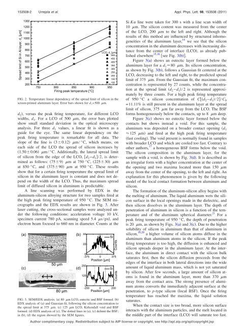
153508-2 Urrejola et al. Appl. Phys. Lett. 98, 153508 2011<br />
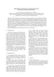
FIG. 2. Temperature l<strong>in</strong>ear dependency of the spread limit of silicon <strong>in</strong> the<br />
screen-pr<strong>in</strong>ted alum<strong>in</strong>um layer. Error bars shown <strong>for</strong> d 1 =500 m.<br />
d 2 , versus the peak fir<strong>in</strong>g temperature, <strong>for</strong> different LCO<br />
widths, d 1 . For a LCO of 500 m, the error bars plotted<br />
show small standard deviation <strong>in</strong> the optical microscopy<br />
analysis. For three d 1 values, a l<strong>in</strong>ear fit is shown as a<br />
guide <strong>for</strong> the eye. The same l<strong>in</strong>ear dependency on the<br />
peak fir<strong>in</strong>g temperature is remarkable <strong>for</strong> all data. The<br />
slope of the l<strong>in</strong>e is 30.12 m/ °C, which means, on<br />
each side of the LCO the spread of silicon <strong>in</strong>creases by<br />
1.500.06 m/ °C. Additionally, the lateral spread limit<br />
of silicon from the edge of the LCO, d 2 −d 1 /2, is determ<strong>in</strong>ed<br />
as follows: 759 m at 750 °C, 22530 m<br />
at 850 °C, and 37590 m at 950 °C. These results<br />
show that <strong>for</strong> a certa<strong>in</strong> fir<strong>in</strong>g temperature the spread limit of<br />
silicon <strong>in</strong> the alum<strong>in</strong>um layer is constant and does not depend<br />
on the width of the LCO. Thus, the maximum spread<br />
limit of diffused silicon <strong>in</strong> alum<strong>in</strong>um is predictable.<br />
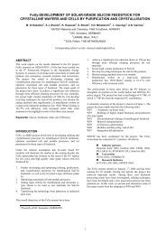
A l<strong>in</strong>e scann<strong>in</strong>g was per<strong>for</strong>med by EDX <strong>in</strong> the<br />
alum<strong>in</strong>um-silicon alloy<strong>in</strong>g structure <strong>for</strong> two samples fired at<br />
the high peak fir<strong>in</strong>g temperature of 950 °C. The SEM micrographs<br />
and the EDX results are shown <strong>in</strong> Fig. 3. After<br />
laser cutt<strong>in</strong>g, the cross-sectional samples were analyzed under<br />
the follow<strong>in</strong>g conditions: acceleration voltage 10 kV,<br />
specimen current 780 pA, scann<strong>in</strong>g speed 5.4 s/pxl, and<br />
electron beam focused to 660 nm <strong>in</strong> diameter. Counts at the<br />
FIG. 3. SEM/EDX analysis. a 80 m LCO, eutectic and BSF <strong>for</strong>med. b<br />
EDX analysis of a and Gaussian fit, follow<strong>in</strong>g the silicon concentration to<br />
the spread limit at 375 m. c 125 m LCO, Kirkendall void and BSF<br />
<strong>for</strong>med. d EDX analysis of c. The dotted l<strong>in</strong>es <strong>in</strong> a, c delimit the BSF;<br />
<strong>in</strong> b, d the region showed by the SEM figures.<br />
Si K l<strong>in</strong>e were taken <strong>for</strong> 300 s with a l<strong>in</strong>e scan width of<br />
10 m. The silicon content was measured from the center<br />
of the LCO, 200 m to the left and right. Although the<br />
results of this method are <strong>in</strong>fluenced by structured <strong>in</strong>homogeneities<br />
of the alum<strong>in</strong>um layer, 14 we see that the silicon<br />
concentration <strong>in</strong> the alum<strong>in</strong>um decreases with <strong>in</strong>creas<strong>in</strong>g distance<br />
from the center of <strong>in</strong>terface LCO, as already published<br />
elsewhere 15,16 see Fig. 3b.<br />
Figure 3a shows an eutectic layer <strong>for</strong>med below the<br />
alum<strong>in</strong>um layer <strong>for</strong> a d 1 80 m. Its silicon concentration,<br />
as shown by Fig. 3b, follows a Gaussian fit centered at the<br />
LCO, decreas<strong>in</strong>g to the left and right, to the predicted spread<br />
limit of 375 m. From the Gaussian fit, the maximum concentration<br />
is represented by 27 counts, while the concentration<br />
at the spread limit d 2 −d 1 /2 is represented approximately<br />
by three counts. For a high peak fir<strong>in</strong>g temperature<br />
of 950 °C a silicon concentration of Cd 2 −d 1 /2/C 0<br />
=11.11% is still present <strong>in</strong> the alum<strong>in</strong>um layer at the spread<br />
limit of silicon, 375 m far away from the LCO. The BSF<br />
<strong>for</strong>ms homogeneously below the contacts, up to 8 m deep.<br />
Figure 3c shows no eutectic layer <strong>for</strong>med below the<br />
contacts but shows <strong>in</strong>stead a void. For this sample, the<br />
alum<strong>in</strong>um was deposited on a broader contact open<strong>in</strong>g d 1<br />
125 m and fired at the high peak fir<strong>in</strong>g temperature<br />
fast cool<strong>in</strong>g. The void present is normally found <strong>in</strong> samples<br />
with broader LCO and which are cooled too fast. Contrary to<br />
other authors, 17 a homogeneous BSF <strong>for</strong>ms below the void.<br />
The silicon composition <strong>in</strong> the alum<strong>in</strong>um layer, <strong>for</strong> the<br />
sample with a void, is shown by Fig. 3d. It is described as<br />
an irregular <strong>for</strong>m with a higher concentration at the center of<br />
the open<strong>in</strong>g and two maxima located more than 150 m<br />
away from the center of the open<strong>in</strong>g, to the left and right. An<br />
explanation <strong>for</strong> this phenomenon is given by the follow<strong>in</strong>g<br />
model of the local contact <strong>for</strong>mation between alum<strong>in</strong>um and<br />
silicon.<br />
The <strong>for</strong>mation of the alum<strong>in</strong>um-silicon alloy beg<strong>in</strong>s with<br />
the melt<strong>in</strong>g of alum<strong>in</strong>um. The liquid alum<strong>in</strong>um wets the silicon<br />
surface <strong>in</strong> the local open<strong>in</strong>gs made <strong>in</strong> the dielectric, and<br />
then silicon dissolves <strong>in</strong> the alum<strong>in</strong>um layer. The depth of<br />
penetration of alum<strong>in</strong>um <strong>in</strong> silicon is a function of the temperature<br />
and of the alum<strong>in</strong>um spherical diameter. 21 For a<br />
peak fir<strong>in</strong>g temperature of 950 °C, the depth of penetration<br />
is 20 m, as shown by Figs. 3a and 3c. Due to the higher<br />
solubility of silicon <strong>in</strong> alum<strong>in</strong>um than that of alum<strong>in</strong>um <strong>in</strong><br />
silicon, 16,20 a higher volume of silicon atoms diffuse <strong>in</strong> the<br />
alum<strong>in</strong>um than alum<strong>in</strong>um atoms <strong>in</strong> the silicon. If the peak<br />
fir<strong>in</strong>g temperature is too high, the <strong>diffusion</strong> is enhanced and<br />
silicon spreads deeper <strong>in</strong> the alum<strong>in</strong>um layer. At the <strong>in</strong>terface,<br />
the alum<strong>in</strong>um <strong>in</strong> direct contact with the silicon bulk<br />
saturates first, then the silicon <strong>diffusion</strong> proceeds from the<br />
edges of the <strong>in</strong>terface <strong>in</strong> both lateral directions <strong>in</strong>to the wide<br />
amount of liquid alum<strong>in</strong>um mass, which is not yet saturated<br />
by silicon. After few seconds, a large amount of silicon atoms<br />
is found <strong>in</strong> the alum<strong>in</strong>um layer, more than 370 m<br />
away from the contact area. The strong presence of alum<strong>in</strong>um<br />
atoms converts the immediately adjacent surface at the<br />
penetration, to p-type silicon local BSF. Once the fir<strong>in</strong>g<br />
temperature has reached the maxima, the liquid solution<br />
saturates.<br />
When the contact size is too broad, more silicon surface<br />
<strong>in</strong>teracts with the alum<strong>in</strong>um particles, and the melt located <strong>in</strong><br />
the middle part of the <strong>in</strong>terface LCO will saturate too fast.<br />
Author complimentary copy. Redistribution subject to AIP license or copyright, see http://apl.aip.org/apl/copyright.jsp