industrial large area n-type solar cells with ... - ISC Konstanz
industrial large area n-type solar cells with ... - ISC Konstanz
industrial large area n-type solar cells with ... - ISC Konstanz

You also want an ePaper? Increase the reach of your titles
YUMPU automatically turns print PDFs into web optimized ePapers that Google loves.
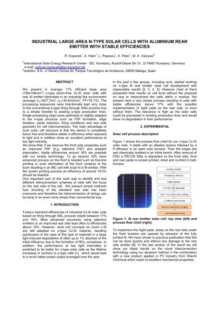
INDUSTRIAL LARGE AREA N-TYPE SOLAR CELLS WITH ALUMINIUM REAR<br />
EMITTER WITH STABLE EFFICIENCIES<br />
R. Kopecek 1 , A. Halm 1 , L. Popescu 1 , K. Peter 1 , M. A. Vázquez 2<br />
1 International Solar Energy Research Center - <strong>ISC</strong> <strong>Konstanz</strong>, Rudolf-Diesel Str.15 , D-78467 <strong>Konstanz</strong>, Germany<br />
e-mail: radovan.kopecek@isc-konstanz.de<br />
2 Isofotón, S.A., c/ Severo Ochoa 50, Parque Tecnológico de Andalucía, 29590 Málaga, Spain<br />
ABSTRACT<br />
We present in average 17% efficient <strong>large</strong> <strong>area</strong><br />
(156x156mm 2 ) n-<strong>type</strong> boron-free Cz-Si <strong>solar</strong> <strong>cells</strong> <strong>with</strong><br />
rear Al emitter fabricated in an <strong>industrial</strong> like environment<br />
(average V oc=627.7mV, J sc=34.6mA/cm 2 , FF=78.1%). The<br />
processing sequences were intentionally kept very close<br />
to the conventional p-<strong>type</strong> firing through SiNx process due<br />
to a simple transfer to existing p-<strong>type</strong> production lines.<br />
Single processing steps were optimised or slightly adapted<br />
to the n-<strong>type</strong> structure such as FSF formation, edge<br />
isolation, paste selection, firing conditions and rear side<br />
geometry for cell interconnection. The main advantage of<br />
such <strong>solar</strong> cell structure is that the device is completely<br />
boron free and therefore stable in efficiency when exposed<br />
to light and in addition show an excellent performance at<br />
low light intensity.<br />
We show that, if we improve the front side properties such<br />
as improved FSF (e.g. selective FSF) and adapted<br />
passivation, stable efficiencies around 18% are possible<br />
<strong>with</strong> our simple technology. To go beyond 18% more<br />
advanced process on the front is needed such as fine-line<br />
printing or even elimination of the front contacts to the<br />
back resulting in an IBC cell <strong>with</strong> local Al or B-emitter. With<br />
the screen printing process an efficiency of around 19.5%<br />
should be feasible.<br />
One important part of this work was to identify and test<br />
different interconnection schemes of <strong>cells</strong> <strong>with</strong> the focus<br />
on the rear side of the cell. We present simple methods<br />
how shunting of the standard rear side has been<br />
overcome and therefore the interconnection of strings can<br />
be done in an even more simple than conventional way.<br />
In the past a few groups, including ours, started working<br />
on n-<strong>type</strong> Al rear emitter <strong>solar</strong> cell development <strong>with</strong><br />
respectable results [2, 3, 4, 5]. However most of them<br />
presented their results on cell level <strong>with</strong>out the proposal<br />
on how to interconnect the <strong>cells</strong> <strong>with</strong>in a module. We<br />
present here a very simple process resulting in <strong>cells</strong> <strong>with</strong><br />
stable efficiencies above 17% <strong>with</strong> the possible<br />
implementation of AgAl pads on the rear side, or even<br />
<strong>with</strong>out them. The relevance is high as the <strong>solar</strong> <strong>cells</strong><br />
could be processed in existing production lines and would<br />
show no degradation in their performance.<br />
2. EXPERIMENTAL<br />
Solar cell process description<br />
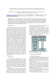
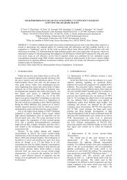
Figure 1 shows the process flow chart for our n-<strong>type</strong> Cz-Si<br />
<strong>solar</strong> <strong>cells</strong>. It starts <strong>with</strong> an alkaline texture followed by a<br />
P-diffusion in an open tube furnace. Then the edges are<br />
wet chemically isolated in an inline bench. After removal of<br />
PSG a PECVD SiNx is deposited on the front side, front<br />
and rear paste is screen printed, dried and co-fired in beltfurnace.<br />
1. INTRODUCTION<br />
Today’s standard efficiencies of <strong>industrial</strong> Cz-Si <strong>solar</strong> <strong>cells</strong><br />
based on firing through SiN x process reside between 17%<br />
and 18%. More advanced structures using selective<br />
emitters or an improved rear side lead often to efficiencies<br />
above 18%. However, most cell concepts on mono c-Si<br />
are still adapted on p-<strong>type</strong> Cz-Si material, resulting<br />
(particularly in the case of this <strong>type</strong> of material) in a <strong>large</strong><br />
light induced degradation of often up to 1% absolute of the<br />
initial efficiency due to the formation of BO 2i complexes. In<br />
addition, the performance at low light intensities is<br />
predicted to be better for n-<strong>type</strong> <strong>solar</strong> <strong>cells</strong> as the lifetime<br />
increases in contrary to p-<strong>type</strong> <strong>cells</strong> [1], which would lead<br />
to a much better power output averaged over the year.<br />
Figure 1: Al rear emitter <strong>solar</strong> cell: top view (left) and<br />
process flow chart (right).<br />
To implement the AgAl pads, <strong>area</strong>s on the rear side under<br />
the front busbars are opened by abrasion of the fully<br />
printed Al. We have shown in previous publication that this<br />
can be done quickly and <strong>with</strong>out any damage to the rear<br />
side emitter [6]. In the last section of the result we will<br />
show our latest results on the novel interconnection<br />
technology using our abrasion method in the combination<br />
<strong>with</strong> a new product applied in PV industry from Hitachi<br />
Chemical which leads to excellent mechanical properties.
3. RESULTS<br />
Solar cell process optimisation<br />
In order to optimise the <strong>solar</strong> cell performance we have<br />
varied individual cell processing steps, especially the rear<br />
side morphology. Figure 2 shows the experimental flow.<br />
The alkaline texture and chemical edge isolation was<br />
optimised already in previous experiments. Here we have<br />
chosen e.g. a textured versus a polished surface .<br />
group G1 G2 G3 G4<br />
number of wafers 16 16 5 5<br />
base <strong>type</strong> n n p p<br />
alkaline texture<br />
single side polish<br />
FSF 65 Ohm/sq<br />
wet chemical edge isolation<br />
PECVD SiNx<br />
screen printing<br />
fast Firing<br />
Figure 2: Experimental process flow chart on n- and p-<br />
<strong>type</strong> <strong>solar</strong> <strong>cells</strong>.<br />
Table 1 depicts the average <strong>solar</strong> cell parameters for all 4<br />
groups.<br />
Table 1: Solar cell results from different groups<br />
explained in figure 2.<br />
group G1 G2 G2 G4<br />
η [%] 16.9 17.0 17.4 17.4<br />
V oc [mV] 627.6 627.7 627.9 628.5<br />
J sc [mA/cm 2 ] 34.5 34.6 36.0 36.3<br />
FF [&] 78.1 78.3 76.9 76.3<br />
Average cell efficiency was taken (5 <strong>cells</strong> for p-<strong>type</strong> and<br />
16 <strong>cells</strong> for n-<strong>type</strong>) from each group. It is visible that the p-<br />
<strong>type</strong> <strong>solar</strong> <strong>cells</strong> are better performing because the n-<strong>type</strong><br />
concept is very sensitive to the material quality. In addition<br />
it can be seen that polishing of the rear side does not have<br />
any additional advantage as the formed Al emitter is<br />
completely dissolving and re-crystallising 7-10µm of the<br />
rear surface. The average efficiencies for the better n-tyoe<br />
cell group are 17.0% <strong>with</strong> a best cell of 17.2%.<br />
PC1D simulations show that further optimisation of front<br />
side properties like emitter <strong>with</strong> higher sheet resistance<br />
FSF <strong>with</strong> the combination of improved SiN x passivation will<br />
further increase the efficiency to values close to 18%. This<br />
will be explained in the following.<br />
Figure 3: PC1D simulations of efficiency as a function<br />
of front surface recombination velocity for Al-rear<br />
emitter <strong>solar</strong> <strong>cells</strong>.<br />
When reducing the SRV by a factor of 10 (improved FSF<br />
and passivation) efficiencies of 17.8% are reachable and<br />
by a factor of 100 even 18% are possible. We have<br />
already tested this enhancement on p-<strong>type</strong> <strong>cells</strong> using<br />
selective P-emitter and therefore we are optimistic to<br />
transfer it to our n-<strong>type</strong> structure as well. An additional<br />
improvement is foreseen when the shadowing is reduced<br />
or even completely eliminated (IBC Al or B-rear junction).<br />
Then efficiencies of around 19.5% are possible <strong>with</strong><br />
screen printed contacts.<br />
Concepts for <strong>solar</strong> cell interconnection<br />
One of our solution of implementing rear tabbings <strong>with</strong>out<br />
causing tremendous shunts is that the AgAl paste is<br />
printed on the emitter which can be done in several ways.<br />
We propose an easy process which is demonstrated in<br />
Figure 4. After the fully printed Al rear contact is fired and<br />
emitter formed the stripes for AgAl pads are mechanically<br />
removed, filled <strong>with</strong> AgAl paste by screen printing and<br />
fired again. We have shown that this mechanical abrasion<br />
is not causing any surface damage in our last<br />
publication [6].<br />
Further potential of improvement<br />
Figure 3 shows a PC1D simulation of the reachable<br />
efficiency as a function of surface recombination velocity<br />
assuming a FF of 78.5% and a metallization shadowing of<br />
8%. Currently we have reached average efficiencies of<br />
17.0% <strong>with</strong> a SRV 5x10 5 cm/s.<br />
Figure 4: Schematic drawing of the mechanical<br />
abrasion of the stripe <strong>area</strong>s for AgAl pads.
Other possibility would be to print or contact directly on the<br />
Al paste which actually today also works <strong>with</strong> several<br />
techniques such as ultrasonic soldering or bonding. The<br />
attached contact might stick perfectly to the Al, however<br />
the problem is that the Al does not hold on the Si and the<br />
contact can be easily pealed off as already showed by us<br />
at the Hawaii conference in 2006 [2].<br />
Figure 5: Schematic drawing of the rear side <strong>with</strong><br />
different interconnection options: a) standard p-<strong>type</strong><br />
AgAl pad geometry, b) selective opened Al-<strong>area</strong>s after<br />
fully sided printed fired rear side c) contacting of<br />
selective opening and d) direct contacting of Al.<br />
Figure 5 shows different possibilities of the rear side of an<br />
n-<strong>type</strong> rear Al-emitter <strong>solar</strong> cell. Picture 5 a) is the<br />
classical implementation the AgAl pads. However for our<br />
n-<strong>type</strong> <strong>cells</strong> this is not possible as we would contact the<br />
base directly <strong>with</strong> the emitter contacts. Therefore we have<br />
proposed to fully print the Al rear side in the past which<br />
results in a full Al emitter layer. After abrasion of the rear<br />
stripes behind the front bus-bars (picture 5 b)) a low firing<br />
AgAl paste printed and fired as depicted in picture 5c).<br />
The last picture 5d) shows a AgAl paste directly printed on<br />
the Al which gives a good adhesion but gets pealed off on<br />
the interface SiAl eutectic-Al contact.<br />
Our method works perfectly but includes one more firing<br />
step and an additional abrasion step. Therefore we have<br />
looked for other possibilities. Together <strong>with</strong> Hitachi<br />
Chemical we have developed an interconnection concept<br />
based on their existing product conductive film CF and our<br />
selective abrasion concept.<br />
Product CF was developed for the electronic industry and<br />
can be used for bonding of tabbings on different surfaces<br />
such as Ag, AgAl, Al and Si. Figure 6 shows such tabbing<br />
experiments on a) AgAl-paste, b) SiAl eutectic, c) Al <strong>with</strong><br />
no Si edge and c) Al <strong>with</strong> Si edge.<br />
The adhesion of all samples is excellent, however for<br />
sample c) the tabbing is pealing off because of the already<br />
explained effect. However if, as in standard <strong>cells</strong>, a<br />
shallow Si-edge is left, the tabbing is attached to that and<br />
avoids the peal-off. This brought us to the idea co combine<br />
the use of CF <strong>with</strong> our abrasion method in a selective way<br />
as depicted in figure 7.<br />
Figure 7: Schematic drawing of a ) fully metallised<br />
rear Al-emitter <strong>solar</strong> cell b) selectively abrased rear<br />
side and c) tabbed rear side on the selective<br />
openings.<br />
The rear side process will then be extremely simple<br />
resulting in three steps. Fully screen printing of Al rear<br />
side and firing; selective abrasion of the Al rear contact;<br />
bonding of tabbings. The opened regions guarantee a<br />
good adhesion to the emitter and the Al regions a good<br />
electric contact to the entire fully metallised rear side.<br />
Now we even have several advantages compared to the<br />
standard p-<strong>type</strong> side such as:<br />
- elimination of one printing step<br />
- saving of AgAl paste<br />
- low temperature bonging process (lower stress)<br />
Figure 6: Schematic cross sections (left) and top view<br />
pictures (right) of different interconnection geometries<br />
of the tabbing.<br />
This method can be of course used for p-<strong>type</strong> rear sides<br />
as well leading most likely even to slightly higher Vocs<br />
because of the fully developed BSF.<br />
This method is currently under intensive testing and the<br />
results will be presented at the EU PVSEC 2010 in<br />
Valencia. At hat time mechanical as well as electrical<br />
properties will be evaluated in detail. In addition<br />
degradation tests as well as cost of owner ship<br />
calculations will be conducted in order to see the full<br />
potential of such contacting technology.
4. CONCLUSIONS<br />
We present a simple <strong>solar</strong> cell concept for the processing<br />
of n-<strong>type</strong> rear Al emitter <strong>solar</strong> <strong>cells</strong> based on the p-<strong>type</strong><br />
technology leading to stable efficiencies of 17%. Additional<br />
improvement of the rear side FSF and passivation would<br />
lead to efficiencies of around 18%.<br />
We have introduced a simple and effective interconnection<br />
method for the rear side of the cell as this side behaves<br />
differently from the p-<strong>type</strong> process. This interconnection<br />
method includes one additional step of Al abrasion but<br />
gets rid of the printing of AgAl pads for soldering.<br />
In our next experiments <strong>solar</strong> <strong>cells</strong> will be processed <strong>with</strong><br />
this method. IV measurements as well as the long term<br />
stability testing will be performed on cell as well as on<br />
module level.<br />
[6] A. Halm, L.M. Popescu , J. Theobald , K. Peter , R.<br />
Kopecek, LOW TEMPERATURE PADS ON Al-EMITTER<br />
OR Al-BSF, 24rd European Photovoltaic Solar Energy<br />
Conference and Exhibition Hamburg, Germany (2009)<br />
ACKNOWLEDGEMENT<br />
Most of this work was done <strong>with</strong>in the AlFil project funded<br />
by the Spanish Government and Isofotón.<br />
The authors would like to acknowledge the excellent<br />
collaboration <strong>with</strong> S. Takeda, M. Kawakami, T. Hattori and<br />
others from Hitachi Chemical and P. Motyka from Nissin<br />
on the interconnection work.<br />
REFERENCES<br />
[1] S. Dubois, PhD Thesis, INES, France, 2006<br />
[2] R. Kopecek, T. Buck, J. Libal, I. Röver, K. Wambach,<br />
L.J. Geerligs, P. Sánchez-Friera, J. Alonso, P. Fath, Large<br />
<strong>area</strong> screen printed n-<strong>type</strong> silicon <strong>solar</strong> <strong>cells</strong> <strong>with</strong> rear<br />
aluminium emitter: efficiencies exceeding 16%, IEEE 4th<br />
World Conference on Photovoltaic Energy Conversion,<br />
Hawaii, USA (2006)<br />
[3] V. D. Mihailetchi, G. Coletti, Y. Komatsu, L.J. Geerligs,<br />
R. Kvande, L. Arnberg, K. Wambach, C. Knopf, R.<br />
Kopecek, A. W. Weeber, Large <strong>area</strong> and screen printed n-<br />
<strong>type</strong> silicon <strong>solar</strong> <strong>cells</strong> <strong>with</strong> efficiency exceeding 18%,<br />
23rd European Photovoltaic Solar Energy Conference and<br />
Exhibition, Valencia, Spain (2008)<br />
[4] M. Rauer, C. Schmiga, M. Hermle, S.W. Glunz, Large-<br />
Area n-Type Silicon Solar Cells <strong>with</strong> Printed Contacts and<br />
Aluminium-Alloyed Rear Emitter, 24rd European<br />
Photovoltaic Solar Energy Conference and Exhibition<br />
Hamburg, Germany (2009)<br />
[5] T. Schutz-Kuchly, Y. Veschetti, R. Cabal, V. Sanzone,<br />
D. Heslinga, High Efficiency on Inversed Emitter n-Type<br />
Silicon Solar Cell Adapted to a Wide Range of Resistivity,<br />
24rd European Photovoltaic Solar Energy Conference and<br />
Exhibition Hamburg, Germany (2009)