Design of a Planar Slotted Waveguide Array Antenna for X-band ...
Design of a Planar Slotted Waveguide Array Antenna for X-band ...
Design of a Planar Slotted Waveguide Array Antenna for X-band ...
- No tags were found...

You also want an ePaper? Increase the reach of your titles
YUMPU automatically turns print PDFs into web optimized ePapers that Google loves.
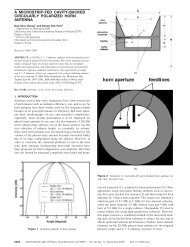
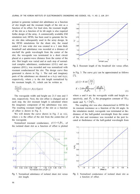
JOURNAL OF THE KOREAN INSTITUTE OF ELECTROMAGNETIC ENGINEERING AND SCIENCE, VOL. 11, NO. 2, JUN. 2011portant to generate isolated slot admittance as a function<strong>of</strong> slot length and the resonant length <strong>of</strong> the slot as afunction <strong>of</strong> its <strong>of</strong>fset. For feed slots, the resonant length<strong>of</strong> the slot as a function <strong>of</strong> its tilt angle is also required<strong>for</strong>the design <strong>of</strong> the array. A commercially available EMsimulation tool, HFSS, has been used to generate the basicslot data subsequently used in the array design. Inthe HFSS simulations <strong>for</strong> the shunt slot, the roundended 2.5 mm wide slot was created in a 1 mm thickbroadwall and admittance was recorded at a distance <strong>of</strong>one-half the guide wavelength from the center <strong>of</strong> theslot; the waveguide was terminated in a short circuitplaced at a quarter-wave distance from the center <strong>of</strong> theslot. Slot length was varied and at each step <strong>of</strong> normalizedcomplex admittance, conductance (G/G r ) and susceptance(B/G r), was recorded and was normalized withresonant conductance<strong>of</strong> the slot. The design curve thusgenerated is shown in Fig. 1. The real and imaginaryparts <strong>of</strong> the admittance are denoted as a h 1(y) and h 2(y),respectively, where y is the slot length normalized bythe resonant length, l/l r , which can be written as( , )Y x lG0( )= h ( y) + jh ( y) g( x)1 2The waveguide width and height are 21.5 mm and 5mm, respectively. Next, the slot <strong>of</strong>fset is changed and ateach step, the slot resonant length is calculated wherethe imaginary component <strong>of</strong> the admittance was zero.The resulting resonant length <strong>of</strong> the slot as a function<strong>of</strong> <strong>of</strong>fset is shown in Fig. 2.We will denote the curve shown in Fig. 2 as v(x),where x is the <strong>of</strong>fset <strong>of</strong> the slot from the center-line <strong>of</strong>the waveguide.Normalized resonant conductance, g ( x) = GrG0, <strong>of</strong>the isolated shunt slot as a function <strong>of</strong> <strong>of</strong>fset is plottedFig. 2. Resonant length <strong>of</strong> the broadwall slot versus <strong>of</strong>fset.in Fig. 3. The curve g(x) can be approximated as follows[7],2 æ p x ög ( x) = K sin ç ÷è a øa b 2 æ pb10 k0öK = 2.09 cos ç ÷b10 k0è 2 ø , (1)where a and b are the waveguide width and height respectively,and b10 is the propagation constant <strong>of</strong> TE 10mode and k0 = 2p l0.The coupling slot was also characterized in HFSS <strong>for</strong>its resonant resistance as a function <strong>of</strong> the tilt angle. Inthe simulation model, waveguide was terminated at thedistance<strong>of</strong> the half-guided wavelength from the center<strong>of</strong> the slot and resistance was recorded at the port locatedat thedistance <strong>of</strong> the half-guided wavelength fromFig. 1. Normalized admittance <strong>of</strong> isolated shunt slot versusslot length.Fig. 3. Normalized conductance <strong>of</strong> isolated shunt slot asa function <strong>of</strong> <strong>of</strong>fset.98