

80960KA EMBEDDED 32-BIT MICROPROCESSOR - Datasheet ...
80960KA EMBEDDED 32-BIT MICROPROCESSOR - Datasheet ...
80960KA EMBEDDED 32-BIT MICROPROCESSOR - Datasheet ...

Create successful ePaper yourself
Turn your PDF publications into a flip-book with our unique Google optimized e-Paper software.
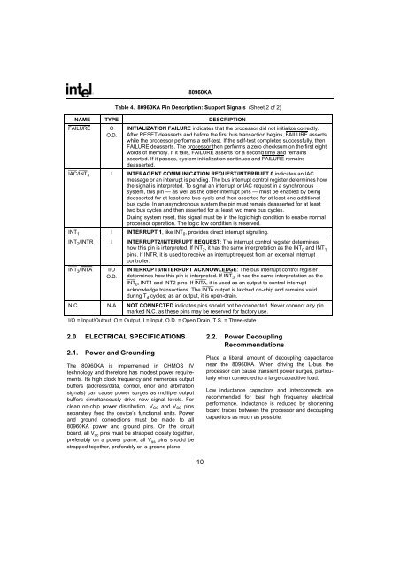
<strong>80960KA</strong>FAILUREOO.D.INITIALIZATION FAILURE indicates that the processor did not initialize correctly.After RESET deasserts and before the first bus transaction begins, FAILURE assertswhile the processor performs a self-test. If the self-test completes successfully, thenFAILURE deasserts. The processor then performs a zero checksum on the first eightwords of memory. If it fails, FAILURE asserts for a second time and remainsasserted. If it passes, system initialization continues and FAILURE remainsdeasserted.IAC/INT 0 I INTERAGENT COMMUNICATION REQUEST/INTERRUPT 0 indicates an IACmessage or an interrupt is pending. The bus interrupt control register determines howthe signal is interpreted. To signal an interrupt or IAC request in a synchronoussystem, this pin — as well as the other interrupt pins — must be enabled by beingdeasserted for at least one bus cycle and then asserted for at least one additionalbus cycle. In an asynchronous system the pin must remain deasserted for at leasttwo bus cycles and then asserted for at least two more bus cycles.During system reset, this signal must be in the logic high condition to enable normalprocessor operation. The logic low condition is reserved.INT 1 I INTERRUPT 1, like INT 0 , provides direct interrupt signaling.INT 2 /INTR I INTERRUPT2/INTERRUPT REQUEST: The interrupt control register determineshow this pin is interpreted. If INT 2 , it has the same interpretation as the INT 0 and INT 1pins. If INTR, it is used to receive an interrupt request from an external interruptcontroller.INT 3 /INTAI/OO.D.Table 4. <strong>80960KA</strong> Pin Description: Support Signals (Sheet 2 of 2)NAME TYPE DESCRIPTIONINTERRUPT3/INTERRUPT ACKNOWLEDGE: The bus interrupt control registerdetermines how this pin is interpreted. If INT 3 , it has the same interpretation as theINT 0 , INT1 and INT2 pins. If INTA, it is used as an output to control interruptacknowledgetransactions. The INTA output is latched on-chip and remains validduring T d cycles; as an output, it is open-drain.N.C. N/A NOT CONNECTED indicates pins should not be connected. Never connect any pinmarked N.C. as these pins may be reserved for factory use.I/O = Input/Output, O = Output, I = Input, O.D. = Open Drain, T.S. = Three-state2.0 ELECTRICAL SPECIFICATIONS2.1. Power and GroundingThe <strong>80960KA</strong> is implemented in CHMOS IVtechnology and therefore has modest power requirements.Its high clock frequency and numerous outputbuffers (address/data, control, error and arbitrationsignals) can cause power surges as multiple outputbuffers simultaneously drive new signal levels. Forclean on-chip power distribution, V CC and V SS pinsseparately feed the device’s functional units. Powerand ground connections must be made to all<strong>80960KA</strong> power and ground pins. On the circuitboard, all V cc pins must be strapped closely together,preferably on a power plane; all V ss pins should bestrapped together, preferably on a ground plane.2.2. Power DecouplingRecommendationsPlace a liberal amount of decoupling capacitancenear the <strong>80960KA</strong>. When driving the L-bus theprocessor can cause transient power surges, particularlywhen connected to a large capacitive load.Low inductance capacitors and interconnects arerecommended for best high frequency electricalperformance. Inductance is reduced by shorteningboard traces between the processor and decouplingcapacitors as much as possible.10


