Dual-Core Intel® Xeon® Processor 5200 Series
Dual-Core Intel® Xeon® Processor 5200 Series
Dual-Core Intel® Xeon® Processor 5200 Series

You also want an ePaper? Increase the reach of your titles
YUMPU automatically turns print PDFs into web optimized ePapers that Google loves.
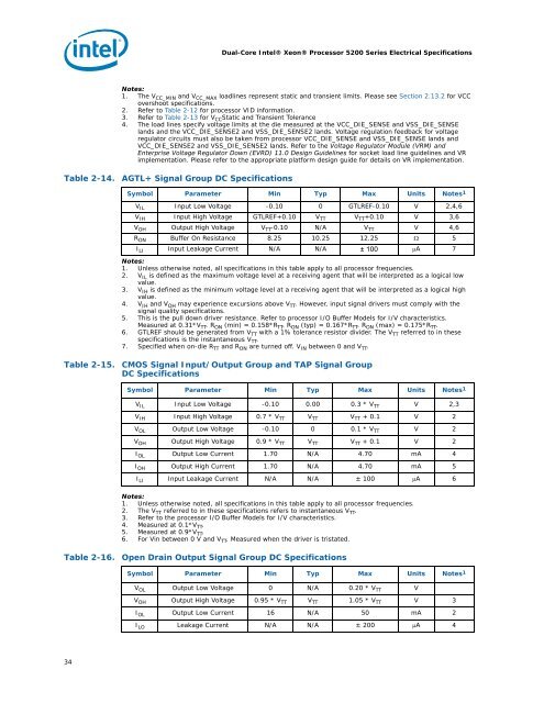
34<br />
<strong>Dual</strong>-<strong>Core</strong> <strong>Intel®</strong> <strong>Xeon®</strong> <strong>Processor</strong> <strong>5200</strong> <strong>Series</strong> Electrical Specifications<br />
Notes:<br />
1. The V CC_MIN and V CC_MAX loadlines represent static and transient limits. Please see Section 2.13.2 for VCC<br />
overshoot specifications.<br />
2. Refer to Table 2-12 for processor VID information.<br />
3. Refer to Table 2-13 for V CCStatic and Transient Tolerance<br />
4. The load lines specify voltage limits at the die measured at the VCC_DIE_SENSE and VSS_DIE_SENSE<br />
lands and the VCC_DIE_SENSE2 and VSS_DIE_SENSE2 lands. Voltage regulation feedback for voltage<br />
regulator circuits must also be taken from processor VCC_DIE_SENSE and VSS_DIE_SENSE lands and<br />
VCC_DIE_SENSE2 and VSS_DIE_SENSE2 lands. Refer to the Voltage Regulator Module (VRM) and<br />
Enterprise Voltage Regulator Down (EVRD) 11.0 Design Guidelines for socket load line guidelines and VR<br />
implementation. Please refer to the appropriate platform design guide for details on VR implementation.<br />
Table 2-14. AGTL+ Signal Group DC Specifications<br />
Symbol Parameter Min Typ Max Units Notes 1<br />
VIL Input Low Voltage -0.10 0 GTLREF-0.10 V 2,4,6<br />
VIH Input High Voltage GTLREF+0.10 VTT VTT+0.10 V 3,6<br />
VOH Output High Voltage VTT-0.10 N/A VTT V 4,6<br />
RON Buffer On Resistance 8.25 10.25 12.25 Ω 5<br />
ILI Input Leakage Current N/A N/A ± 100 μA 7<br />
Notes:<br />
1. Unless otherwise noted, all specifications in this table apply to all processor frequencies.<br />
2. V IL is defined as the maximum voltage level at a receiving agent that will be interpreted as a logical low<br />
value.<br />
3. V IH is defined as the minimum voltage level at a receiving agent that will be interpreted as a logical high<br />
value.<br />
4. V IH and V OH may experience excursions above V TT . However, input signal drivers must comply with the<br />
signal quality specifications.<br />
5. This is the pull down driver resistance. Refer to processor I/O Buffer Models for I/V characteristics.<br />
Measured at 0.31*V TT . R ON (min) = 0.158*R TT . R ON (typ) = 0.167*R TT . R ON (max) = 0.175*R TT .<br />
6. GTLREF should be generated from V TT with a 1% tolerance resistor divider. The V TT referred to in these<br />
specifications is the instantaneous V TT .<br />
7. Specified when on-die R TT and R ON are turned off. V IN between 0 and V TT .<br />
Table 2-15. CMOS Signal Input/Output Group and TAP Signal Group<br />
DC Specifications<br />
Symbol Parameter Min Typ Max Units Notes 1<br />
VIL Input Low Voltage -0.10 0.00 0.3 * VTT V 2,3<br />
VIH Input High Voltage 0.7 * VTT VTT VTT + 0.1 V 2<br />
VOL Output Low Voltage -0.10 0 0.1 * VTT V 2<br />
VOH Output High Voltage 0.9 * VTT VTT VTT + 0.1 V 2<br />
IOL Output Low Current 1.70 N/A 4.70 mA 4<br />
IOH Output High Current 1.70 N/A 4.70 mA 5<br />
ILI Input Leakage Current N/A N/A ± 100 μA 6<br />
Notes:<br />
1. Unless otherwise noted, all specifications in this table apply to all processor frequencies.<br />
2. The V TT referred to in these specifications refers to instantaneous V TT .<br />
3. Refer to the processor I/O Buffer Models for I/V characteristics.<br />
4. Measured at 0.1*V TT .<br />
5. Measured at 0.9*V TT .<br />
6. For Vin between 0 V and V TT . Measured when the driver is tristated.<br />
Table 2-16. Open Drain Output Signal Group DC Specifications<br />
Symbol Parameter Min Typ Max Units Notes 1<br />
VOL Output Low Voltage 0 N/A 0.20 * VTT V<br />
VOH Output High Voltage 0.95 * VTT VTT 1.05 * VTT V 3<br />
IOL Output Low Current 16 N/A 50 mA 2<br />
ILO Leakage Current N/A N/A ± 200 μA 4