Dual-Core Intel® Xeon® Processor 5200 Series
Dual-Core Intel® Xeon® Processor 5200 Series
Dual-Core Intel® Xeon® Processor 5200 Series

Create successful ePaper yourself
Turn your PDF publications into a flip-book with our unique Google optimized e-Paper software.
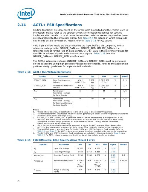
2.14 AGTL+ FSB Specifications<br />
36<br />
<strong>Dual</strong>-<strong>Core</strong> <strong>Intel®</strong> <strong>Xeon®</strong> <strong>Processor</strong> <strong>5200</strong> <strong>Series</strong> Electrical Specifications<br />
Routing topologies are dependent on the processors supported and the chipset used in<br />
the design. Please refer to the appropriate platform design guidelines for specific<br />
implementation details. In most cases, termination resistors are not required as these<br />
are integrated into the processor silicon. See Table 2-8 for details on which signals do<br />
not include on-die termination. Please refer to Table 2-18 for R TT values.<br />
Valid high and low levels are determined by the input buffers via comparing with a<br />
reference voltage called GTLREF_DATA and GTLREF_ADD. GTLREF_DATA is the<br />
reference voltage for the FSB 4X data signals, GTLREF_ADD is the reference voltage for<br />
the FSB 2X address signals and common clock signals. Table 2-18 lists the<br />
GTLREF_DATA and GTLREF_ADD specifications.<br />
The AGTL+ reference voltages (GTLREF_DATA and GTLREF_ADD) must be generated<br />
on the baseboard using high precision voltage divider circuits. Refer to the appropriate<br />
platform design guidelines for implementation details.<br />
Table 2-18. AGTL+ Bus Voltage Definitions<br />
Symbol Parameter Min Typ Max Units Notes 1<br />
GTLREF_DATA Data Bus Reference<br />
Voltage<br />
GTLREF_ADD Address Bus Reference<br />
Voltage<br />
R TT<br />
R TT<br />
Termination<br />
Resistance (pull up)<br />
for Data Signals<br />
Termination<br />
Resistance (pull up)<br />
for Common Clock and<br />
Address Signals<br />
0.98 *<br />
0.667 * V TT<br />
0.98 *<br />
0.667 * V TT<br />
0.667 *<br />
VTT 0.667 *<br />
VTT 1.02*0.667<br />
* VTT 1.02*0.667<br />
* VTT V 2, 3<br />
V 2, 3<br />
43 49 55 Ω 4, 5<br />
40 49 58 Ω 4, 6<br />
Notes:<br />
1. Unless otherwise noted, all specifications in this table apply to all processor frequencies.<br />
2. The tolerances for this specification have been stated generically to enable system designer to calculate the<br />
minimum values across the range of V TT .<br />
3. GTLREF_DATA and GTLREF_ADD is generated from V TT on the baseboard by a voltage divider of 1%<br />
resistors. The minimum and maximum specifications account for this resistor tolerance. Refer to the<br />
appropriate platform design guidelines for implementation details. The V TT referred to in these<br />
specifications is the instantaneous V TT .<br />
4. R TT is the on-die termination resistance measured at V OL of the AGTL+ output driver. Measured at<br />
0.31*V TT. R TT is connected to V TT on die. Refer to processor I/O Buffer Models for I/V characteristics.<br />
5. This specified range is also applicable for the DP[3:0]# and DRDY# Common Clock signals. Refer to<br />
Table 2-6 and Table 2-7 for AGTL+ signal grouping and details on signals that include on-die termination<br />
6. The DP[3:0]# and DRDY# Common Clock signals are not included in this range. Refer to Table 2-6 and<br />
Table 2-7 for AGTL+ signal grouping and details on signals that include on-die termination.<br />
Table 2-19. FSB Differential BCLK Specifications (Sheet 1 of 2)<br />
Symbol Parameter Min Typ Max Unit Figure Notes 1<br />
VL Input Low Voltage -0.150 0.0 0.150 V 2-10<br />
VH Input High Voltage 0.660 0.710 0.850 V 2-10<br />
VCROSS(abs) Absolute Crossing Point 0.250 0.350 0.550 V 2-10,<br />
2-11<br />
V CROSS(rel) Relative Crossing Point 0.250 +<br />
0.5 *<br />
(V Havg -<br />
0.700)<br />
Δ VCROSS<br />
Range of Crossing<br />
Points<br />
N/A 0.550 +<br />
0.5 *<br />
(V Havg -<br />
0.700)<br />
V 2-10,<br />
2-11<br />
N/A N/A 0.140 V 2-10,<br />
2-11<br />
2,9<br />
3,8,9,11