UNIVERSITI TEKNOLOGI MALAYSIA - FKE - UTM
UNIVERSITI TEKNOLOGI MALAYSIA - FKE - UTM
UNIVERSITI TEKNOLOGI MALAYSIA - FKE - UTM

Create successful ePaper yourself
Turn your PDF publications into a flip-book with our unique Google optimized e-Paper software.
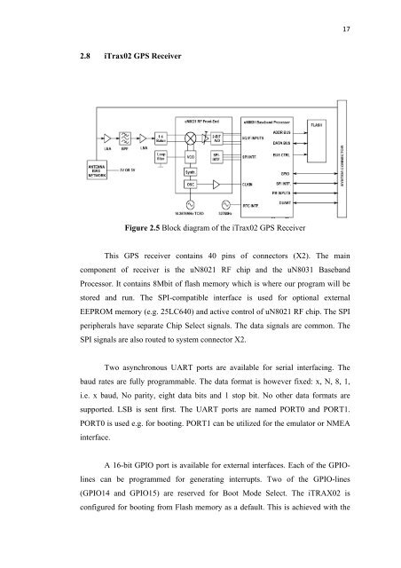
172.8 iTrax02 GPS ReceiverFigure 2.5 Block diagram of the iTrax02 GPS ReceiverThis GPS receiver contains 40 pins of connectors (X2). The maincomponent of receiver is the uN8021 RF chip and the uN8031 BasebandProcessor. It contains 8Mbit of flash memory which is where our program will bestored and run. The SPI-compatible interface is used for optional externalEEPROM memory (e.g. 25LC640) and active control of uN8021 RF chip. The SPIperipherals have separate Chip Select signals. The data signals are common. TheSPI signals are also routed to system connector X2.Two asynchronous UART ports are available for serial interfacing. Thebaud rates are fully programmable. The data format is however fixed: x, N, 8, 1,i.e. x baud, No parity, eight data bits and 1 stop bit. No other data formats aresupported. LSB is sent first. The UART ports are named PORT0 and PORT1.PORT0 is used e.g. for booting. PORT1 can be utilized for the emulator or NMEAinterface.A 16-bit GPIO port is available for external interfaces. Each of the GPIOlinescan be programmed for generating interrupts. Two of the GPIO-lines(GPIO14 and GPIO15) are reserved for Boot Mode Select. The iTRAX02 isconfigured for booting from Flash memory as a default. This is achieved with the