
You also want an ePaper? Increase the reach of your titles
YUMPU automatically turns print PDFs into web optimized ePapers that Google loves.
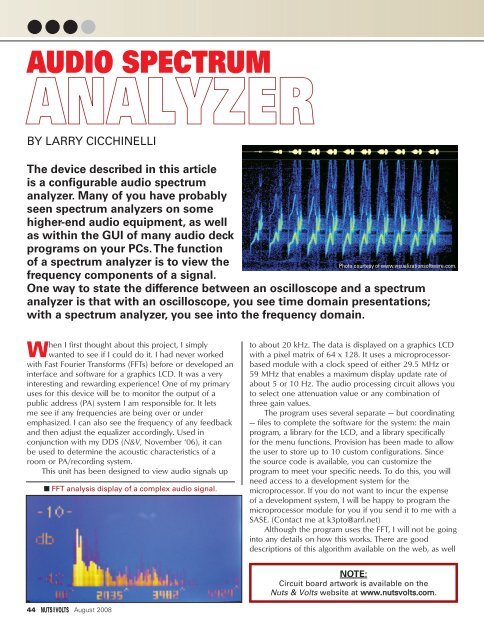
●●●●AUDIO SPECTRUMANALYZERBY LARRY CICCHINELLIThe device described in this articleis a configurable audio spectrumanalyzer. Many of you have probablyseen spectrum analyzers on somehigher-end audio equipment, as wellas within the GUI of many audio deckprograms on your PCs.The functionof a spectrum analyzer is to view thefrequency components of a signal.One way to state the difference between an oscilloscope and a spectrumanalyzer is that with an oscilloscope, you see time domain presentations;with a spectrum analyzer, you see into the frequency domain.Photo courtesy of www.visualizationsoftware.com.When I first thought about this project, I simplywanted to see if I could do it. I had never workedwith Fast Fourier Transforms (FFTs) before or developed aninterface and software for a graphics LCD. It was a veryinteresting and rewarding experience! One of my primaryuses for this device will be to monitor the output of apublic address (PA) system I am responsible for. It letsme see if any frequencies are being over or underemphasized. I can also see the frequency of any feedbackand then adjust the equalizer accordingly. Used inconjunction with my DDS (N&V, November ‘06), it canbe used to determine the acoustic characteristics of aroom or PA/recording system.This unit has been designed to view audio signals up■ FFT analysis display of a complex audio signal.to about 20 kHz. The data is displayed on a graphics LCDwith a pixel matrix of 64 x 128. It uses a microprocessorbasedmodule with a clock speed of either 29.5 MHz or59 MHz that enables a maximum display update rate ofabout 5 or 10 Hz. The audio processing circuit allows youto select one attenuation value or any combination ofthree gain values.The program uses several separate — but coordinating— files to complete the software for the system: the mainprogram, a library for the LCD, and a library specificallyfor the menu functions. Provision has been made to allowthe user to store up to 10 custom configurations. Sincethe source code is available, you can customize theprogram to meet your specific needs. To do this, you willneed access to a development system for themicroprocessor. If you do not want to incur the expenseof a development system, I will be happy to program themicroprocessor module for you if you send it to me with aSASE. (Contact me at k3pto@arrl.net)Although the program uses the FFT, I will not be goinginto any details on how this works. There are gooddescriptions of this algorithm available on the web, as wellNOTE:Circuit board artwork is available on the<strong>Nuts</strong> & <strong>Volts</strong> website at www.nutsvolts.com.44 August 2008
as others that transform between the time domain and thefrequency domain. There is a good primer of the DFT inthe October ‘07 issue of <strong>Nuts</strong> & <strong>Volts</strong>.This device is relatively small, fitting into an enclosureof about 6.8” x 4.8” x 2.5”, and is powered by a DC wallwart between 9V and 15V. Someone who is better atpackaging than I am could probably fit it into a smallerenclosure. I tried a 4.5” square box but could not quitemake it work.The main thrust of this article is to describe each ofthe circuits, some of the software, and the construction ofthe system. Complete construction information, includingthe bill of materials (BOM), schematics, and printed circuitboard (PCB) details can be found on my website atWWW.QSL.NET/k3pto under the heading “Audio FFTdisplay.” The source code for the main program andthe libraries are also on my website, as well as atwww.nutsvolts.com.The three circuit boards embody of the following:power supply and processor; analog circuits; and theinterface for the graphics LCD. I could have put the LCDinterface on the same board as the processor but Idecided to make it a separate board for two reasons: (1) itallows the LCD to be ported to other projects more easily;and (2) the board has very fine and closely spaced traces(.020” pitch). I felt it would be advantageous to have aseparate board just in case the first assembly attempt fails.Then only this board would be affected — see theConstruction Notes elsewhere in this article.Figure 1 is a block diagram of the system. Note thatthe controlpath to the display and the ADC are over SPI(Synchronous Peripheral Interface). This is a serial communicationsprotocol designed by Motorola in the 1960s. It isa popular method of enabling a microprocessor tocommunicate with peripheral devices, usually on the samecircuit board. With SPI, you can controlseveral devices connected to thecontroller via a serial bus that has thefollowing signals: Clock, Data In, andData Out. Each controlled device alsorequires a separate Chip Select signal.When implementing an SPIsystem with multiple devices, youneed to make sure that the properphase relationship (there are fourpossibilities) between the clock and thedata is maintained for each device. Inthis system, both devices use thesame clock to data phasing. Oneproject I built (see N&V November‘06) used two devices from the samemanufacturer that had different clockto data phasing so I had to adjust thephase each time I initiated communicationswith one of them and thenput it back when done.The power supply (Figure 2)■ FIGURE 1. FFTblock diagram.contains two series regulators: 5V and 3.3V. The 5V isused by the analog circuits and the 3.3V by the microprocessorand LCD. The output of the 5V regulator is alsothe source for the 3.3V regulator. The series resistor, R1,reduces the power dissipation of the 5V regulator. If youwant to optimize the circuit a little, you can change theresistor based on the wall wart you use. The analog circuitcurrent is about 20 mA (mostly due to the relay) and the3.3V current is either 70 mA or 140 mA, depending onthe processor board you are using. You have to have atleast 7V on the input of the 5V regulator for properoperation. With a 10 ohm resistor, the voltage drop with200 mA will be about 2V. So, a 9V wall wart is sufficientto power the unit that uses the faster processor. If youchoose to use the slower processor, then a 20 ohmresistor will be a better choice. Be sure to get a resistorwith the appropriate power rating.There are two main functions the Input Amplifier/■ FIGURE 2. The powersupply module.August 2008 45
they are the same cost as 5% values (asSMD resistors). Also, an error of 1% isequivalent to only 0.09 db.There are two procedures that mustbe used to calibrate the ADC and theFFT processing:1) Measure the no-signal DC offset voltage.You can do this by simply not activating K1and not applying an input signal. Also, eachof the analog switches must be turned on sothat the gain of each of the three stages isone. The voltage will be very close to 2.5Vand is subtracted from all the readings inorder to present the FFT algorithm with aseries of values centered on 0 volts — arequirement of the algorithm. This ADCvalue — that should be close to 2048 — isstored into the configuration memory area.Note that there is an adjustmentpotentiometer for each of the gain circuits.These are required due to the offsetvoltages and currents of the op-amps. Thereis a menu option that allows you to activate anddeactivate the analog switches so that you can use thepotentiometers to “balance” the output voltage to thesame value whether or not the switch is activated. When■ FIGURE 4. The 22 kHzlow pass filter.done, the voltage should be very close to +2.5V,independent of the selected gain.2) Measure the processed signal amplitude of a single■ FIGURE 5. The digitalmicroprocessor section.August 2008 47
■ The analog and digital boards. The digitalboard has the RCM4120 inserted.The maximum signal presented to the ADC must beless than 5V peak-to-peak, about 1.7 VRMS. I suggest thatyou use 0.7 VRMS as a standard because it is equivalentto 2.0V peak-to-peak, as well as 0 dBm into 500Ω andmakes a nice reference value. You could also use 1 VRMSsince this would be 2.828V peak-to-peak. Both leave a little“headroom,” but not a whole lot. Theresistor values I show on the schematic arebased on the following two examples.frequency sine wave input. This procedure allows you toadjust the input signal amplitude and will store both theprocessed and unprocessed amplitudes. I suggest 0 dBmor 1 VRMS — see the discussion that follows. Thecalibration function displays the value of the input signalyou are using for calibration so that you can monitor itwhile adjusting it. This yields the best calibration for thesystem.Note: The “processed” amplitude is the output valueof the FFT algorithm.■ FIGURE 6.The LCD andits connections.48 August 20081) Suppose you want to monitor theoutput of a 100W power amplifier that isdriving an eight ohm speaker. The outputvoltage at full power is therefore: V =sqrt(100*8) = 28.3 VRMS. In order tomeasure this signal, you need to divide itby 28. A set of “reasonable” resistors isthen: R1 = 2.7K and R2 = 100 ohms. Ihave designed the circuit board so that R2is an SMD and R1 is a thru-hole part so itcan be 1/2 watt. By not activating K1, theattenuator will be used giving the overallcircuit a “gain” of 1/28. There is adisadvantage to this circuit — it gives the audio circuit aninput resistance of 2.8K. If this is not acceptable, you canincrease the resistor values — but not too much or theratio will be affected by R5 and R6.2) Now, suppose you want to monitor a signal that is 100mVRMS. All you have to do is multiply it by 10. Using thevalues shown in the schematic: With IC3 turned off, thegain is (1K+9K)/1K that is a voltage gain of 10 (20 db);with IC3 turned on, R11 is shorted out that would yielda gain of 1 (0 db).The program has a feature that causes it to readcalibration values from its Flash memory when it firststarts. I have set up the program so that if it detects thatno calibration values have been previously stored, it willuse default values that should be very close — assumingthe circuit is built with thevalues in the schematics.The circuit has enough gainfor a typical microphone if youuse the suggested transformer.Most mics have an outputvoltage of about -60 dbm (0.7mV into 500Ω). The transformerhas a gain of about 12 db, sowith the available gain of 50 dbthat should be adequate formost mics. Note that there isalso voltage available for micsthat need phantom power. Thisshould be applied to the primaryof the transformer asshown in Figure 7.One of the requirements ofthe FFT is that you must samplethe input signal at least twice as
■The LCD interface board showing the fine pitchconnector and copper traces.fast as the highest frequency being analyzed. Thissampling frequency is called the Nyquist limit afteran early developer of sampling theory. One of theanomalies of the FFT is that input frequenciesabove one half the sampling frequency will be“mirrored” into the lower frequency range of theresults. For instance, if the sampling frequency is40 kHz, the highest input frequency that shouldbe applied is 20 kHz. However, if a signal of 21kHz is applied, it will be displayed as if it were 19kHz. This is one of the limitations of this system.There are two ways of getting around this: (1)insert a low pass filter with a sharp cutoff at thehighest frequency of interest; or (2) sample at ahigher rate than necessary. The disadvantage of thelow pass filter is that it should be programmable.The disadvantage of the high sampling rate islower resolution. The resolution of the system can becalculated as follows: Resolution = SampleFrequency/(2*Sample Size). The factor of 2 is due to theFFT algorithm that I am using.I have decided to include an active low pass filter(Figure 4) with a cutoff frequency of 22 kHz. The filter is afour pole Sallen-Key design and can easily be bypassed ifyou do not want to include it. The design I used wasfound at http://beis.de/Elektronik/Filter/ActiveLPFilter.html. This site allows you to modify the characteristics ofthe filter on-line and calculates new values for you. I haveno idea how sensitive the filter characteristics are relativeto the component values. However, I did measure theresponse of the filter in the circuit and it is quite good:at 20 kHz it has about 1.2 db loss; at 24 kHz it is about4 db. I suggest that you use a sampling frequency ofabout 45 kHz if you are going to analyze signals withfrequency components up to 20 kHz. This should allowthe filter to remove most — if not all — of the higherfrequency artifacts. Another limitation of the system is thedisplay frequency resolution; 100 columns are used forthe FFT display. Based on the formula above for resolution,at a sample frequency of 45 kHz and a sample size of512, the resolution is 43.9 Hz. Since the data is displayedin 100 columns, that essentially means that the total spanof frequencies displayed must be a multiple of 100 *43.9or 4390 Hz. In practical terms, this says that if you tell thesystem that you want an upper frequency of 10 kHzdisplayed, you will actually get 4390*3 or 13.2 kHz.My original design had the analog circuits on thesame board as the processor. I decided to move them to aseparate board for two reasons: (1) to keep digital noise■ FIGURE 7.An overview ofthe enclosurewiring.August 2008 49
PARTS LISTITEM PART NUMBER QTY❑ Housing 103158** (Jameco) 2❑ Socket pins 100766** (Jameco) 55❑ Header 160882 * (Jameco) 2❑ PB switch 104-0013-EVX 4❑ SPST switch 108-1MS1T1B1M1QE-EVX 1❑ SPDT switch 108-1MS1T1B1M1QE-EVX 1❑ Power connector 163-2325-E 1❑ Power connector 1710-2532 1❑ 3.5 mm Phone jack 161-7300-EX 1❑ XLR3-F 164-7133 1❑ 1/4” Phone jack 16PJ022 1❑ Phono jack 16PJ052 1❑ 1/4” Phone jack 16PJ080 1❑ 10Ω 2W 282-10-RC 1❑ 1K 292-1.0K-RC 10❑ 1M 292-1.0M-RC 1❑ 1.7K 292-1.7K-RC 1❑ 100K 292-100K-RC 1❑ 100 292-100-RC 2❑ 10K 292-10K-RC 12❑ 19.6K 292-19.6K-RC 1❑ 2.1K 292-2.10K-RC 1❑ 20.5K 292-20.5K-RC 1❑ 3.3K 292-3.3K-RC 1❑ 3.57K 292-3.57K-RC 2❑ 332K 292-332K-RC 1❑ 47K 292-47K-RC 1❑ 5.49K 292-5.49K-RC 1❑ 8.06K 292-8.06K-RC 1❑ 9K 292-9.09K-RC 1❑ 100Ω 30BJ250-100 1❑ 2.7K 30BJ500-2.7K 1❑ 42TL019 42TL019 1❑ TS912 511-TS912BID 3❑ FAN1616 512-FAN1616AD33X 1❑ GF1A 512-GF1A 2❑ 7805 512-KA7805ATU 1❑ Socket 538-52437-3072 1❑ Socket 571-5-104652-5 1❑ 220 pf 581-08051A221K 1❑ .0022 µF 581-08053A222K 1❑ 470 pf 581-08055A471K 1❑ 680 pf 581-08055A681K 1❑ .47 µF 581-0805ZC474K 8❑ Enclosure 377-1163-ND (Digi-Key) 1❑ 2N3904 625-2N3904 2❑ 100 µF 647-UVR1E101MED 1❑ 20K 72-T93YA-20K 3❑ F-51553 805-F51553GNBJAEN 1❑ Relay 806-9081C1-05-00 1❑ 1.0 µF 80-C1206C105K3R 5❑ 4.7 µF 80-C1206C475Z4V 4❑ ADS7816 ADS7816U-ND (Digi-Key) 1❑ Microprocessor RCM4120 1❑ SN74LVC1G66DBVR 296-13253-1-ND (Digi-Key) 3❑ LED 606-CMD3750 1* 160882 Headers are cut to size and require 100766 pinsand housing** 100766 socket pins requires 103158 housing cut to sizeThe system needs about 55 total pins — this is equivalent totwo pieces each of 103158 and 160882NOTE: All items are from Mouser unless stated otherwise.A more detailed parts list is available at www.nutsvolts.com.50 August 2008away from the analog amplification stages as muchas possible; and (2) to enable the flexibility in theaudio processing so the builder can develop his/herown circuit and control it from the system.The processor circuit (Figure 5) shows theconnections from the microprocessor board to theother circuits. The board also has the A-to-Dconverter and the pull-up resistors for the switches.The ADC is powered by the 5V regulator. Assuch, its SPI output signal is a 5V logic level. Themicroprocessor board I am using can handle only3.3V input signals — that is why there is a voltagedivider on the output of the ADC.I have selected a 2 MHz clock speed for theSPI system. This is used for both the analogconverter and the display. The interrupt serviceroutine that is used to sample the input signal takesapproximately 12 to 16 µs, depending on theprocessor you are using. This means that thehighest theoretical sampling frequency is either80 kHz or 60 kHz. The fastest sample rate the ADCwill support is 200 kHz. This is equivalent to an SPIclock rate of 3.2 MHz since it takes 16 SPI clocksto read the converter. The display can handle abouta 7 MHz clock. So, I could increase the clockspeed to 3 MHz and get a 50% increase in thesample rate. However, this is not necessary sincethe system is designed for the audio spectrum.All of the values can be modified via the menusystem can be stored in the Flash memory of themicroprocessor board. This includes the ADCcalibration, the frequency “window” you wantto view, sample size, etc. The current menusystem allows you to store up to 10 sets of thesevalues. There is a complete and detaileddescription of the menu system on my website atwww.qsl.net/k3pto.Some Construction NotesA few comments about the BOM. Althoughthe BOM shows mostly Mouser part numbers,many of them are available from other sources,including Digi-Key and Jameco. If you want to savesome money, I suggest you search the sites for thebest prices on the higher cost items. Bear in mindthat these companies may have a minimum dollarvalue for orders. Many of the parts for this projectdo not have critical values. For instance, the gainresistors in the analog circuit may be customizedfor your application. The transistor type used forK1 on the analog board and the backlight on thedigital board can be any small signal NPN oreven an FET (2N7000). The PCBs (three) can bepurchased from FAR Circuits as a set.I recommend that you purchase two of theLCD boards, as well as two of the LCD connectors.
Soldering the LCD connector to the board is the most difficultpart of this project. I highly recommend using a 3X,lighted magnifying lens (5X would be better). I also used a10X eye loupe to make sure of the connections and thatthere were no shorts. Soldering with a very fine tip isrequired — I use a .030” tip. One suggestion forsoldering is to tin the leads of the connector using finesolder, align the connector, solder the tab near pin 1 tokeep it in place, then heat the pins with a clean solderingiron tip. This method takes advantage of the tinned circuitboard and prevents the application of too muchsolder that could create shorts between pins. I highlyrecommend that you use .015” solder; using thicker solderwill probably cause you to create shorts between adjacentpins. You should also have some solder wick on hand.I like to use single row pin headers for my I/Oconnections. Their cost is about $.15 per point if you buyenough to do 100 points. I like this method because itallows me to disconnect all the sub-systems. If you do notwant to use these connectors, you can easily just solderwires into the header location points. If you do use theconnectors, I suggest that if you are hand crimping, youkeep the socket pins on the strip while crimping with asmall pair of needle-nose pliers. A better solution is tohave a crimp tool available — but these are somewhatexpensive. Whatever method you use, you shouldstrip 1/8” of insulation off each end to make a goodconnection.You need mount only the input sockets you need foryour application instead of all the ones I have shown inthe enclosure schematic (Figure 7). The schematic doesnot show any connections to the high level input (H2).You can mount and connect any appropriate sockets yourapplication requires. Another possibility is to use a switchto connect J3 to either H1 or H2 of the analog board.You may use whatever switches you like for the powerand pushbutton switches. I selected ones from the Mousercatalog based primarily on cost.My website has a number of JPEG files to aid you inassembling the circuit boards. There are three files for theanalog and digital boards and two for the LCD board.These files include: top side silk screen, bottom sidesilk screen, and vias. The silk screen files show partsplacement and the via files show the locations of the vias.The via locations are needed because my vendor for theboards does not do plated-thru holes. You will have toinsert wire jumpers in all the via locations. This alsomeans that a number of components need to besoldered on both sides of the boards in order to completethe circuits.The wiring between the subsystems should be donewith fairly flexible wire. I happen to have a supply of eightconductor telephone cable. This is an advantage becauseit is multi-color that makes tracing signals easier. I was ableto use this effectively by first cutting the cable to therequired length, then removing the wires from the outersheath. Let me know how your build goes. NVAugust 2008 51