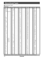
Burr Brown PCM1738 - 24-Bit, 192kHz Sampling.pdf - MaxDat
Burr Brown PCM1738 - 24-Bit, 192kHz Sampling.pdf - MaxDat
Burr Brown PCM1738 - 24-Bit, 192kHz Sampling.pdf - MaxDat

Create successful ePaper yourself
Turn your PDF publications into a flip-book with our unique Google optimized e-Paper software.
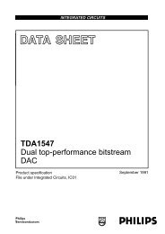
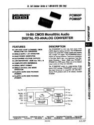
V CC 1BLOCK DIAGRAMLRCKDATABCKInputI/FCurrentSegmentDACI OUT L+I OUT L–RSTMUTECSMCFunctionControl8xOversamplingDigitalFilterandFunctionControlAdvancedSegmentDACModulatorBiasand V REFV COM 2I REFV COM 1V COM 3IV and FilterIV and FilterMDIMDOI/FCurrentSegmentDACI OUT R–I OUT R+System ClockSCKISystem ClockManagerZERO DetectPower SupplyV CC2SCKOZEROLZERORV DDDGNDV CC 3AGND1AGND2PIN CONFIGURATIONPIN ASSIGNMENTSTOP VIEWSSOPPIN NAME TYPE FUNCTIONRSTZEROLZERORLRCKDATABCKSCKIDGNDV DDSCKOMDOMDIMCCS1234567891011121314<strong>PCM1738</strong>28272625<strong>24</strong>232221201918171615V CC 3AGND2I OUT L–I OUT L+V CC 2V CC 1V COM 3I REFV COM 2V COM 1AGND1I OUT R+I OUT R–MUTE1 RST IN Reset (1)2 ZEROL OUT Zero Flag for L-Channel.3 ZEROR OUT Zero Flag for R-Channel.4 LRCK IN Left/Right clock (f S ) input for normal operation. (1)WDCK clock input in external DF mode. Connectedto GND in DSD mode.5 DATA IN Serial Audio data input for normal operation. (1)L-channel audio data input for external DF andDSD modes.6 BCK IN <strong>Bit</strong> Clock. Input. Connected to GND for DSD mode. (1)7 SCKI IN System Clock Input for normal operation. (1)BCK (64f S ) clock input for DSD mode.8 DGND – Digital Ground9 V DD – Digital Supply, +3.3V10 SCKO OUT System Clock Output11 MDO OUT Serial data output for function control register. (2)12 MDI IN Serial data input for function control register. (1)13 MC IN Shift Clock for function control register. (1)14 CS IN Mode Control chip select and latch signal. (1)15 MUTE IN Analog output mute control for normal operation. (1)R-channel audio data input for external DF andDSD modes.16 I OUT R– OUT R-Channel Analog Current Output –17 I OUT R+ OUT R-Channel Analog Current Output +18 AGND1 – Analog Ground19 V COM 1 – Internal Bias Decoupling Pin20 V COM 2 – Common Voltage for I/V21 I REF – Output current reference bias pin. Connect 16kΩresistor to GND.22 V COM 3 – Internal Bias Decoupling Pin23 V CC 1 – Analog Supply, +5.0V<strong>24</strong> V CC 2 – Analog Supply, +5.0V25 I OUT L+ OUT L-Channel Analog Current Output +26 I OUT L– OUT L-Channel Analog Current Output –27 AGND2 – Analog Ground28 V CC 3 – Analog Power Supply, +5.0VNOTES: (1) Schmitt-trigger input, 5V tolerant. (2) Tristate output.4<strong>PCM1738</strong>SBAS174A