CHI030B PICAXE-18 STANDARD PROJECT BOARD
CHI030B PICAXE-18 STANDARD PROJECT BOARD
CHI030B PICAXE-18 STANDARD PROJECT BOARD

You also want an ePaper? Increase the reach of your titles
YUMPU automatically turns print PDFs into web optimized ePapers that Google loves.
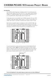
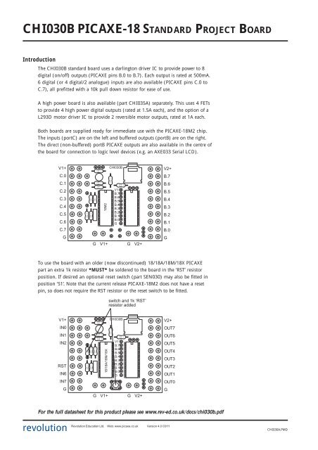
<strong>CHI030B</strong> <strong>PICAXE</strong>-<strong>18</strong> <strong>STANDARD</strong> <strong>PROJECT</strong> <strong>BOARD</strong>IntroductionThe <strong>CHI030B</strong> standard board uses a darlington driver IC to provide power to 8digital (on/off) outputs (<strong>PICAXE</strong> pins B.0 to B.7). Each output is rated at 500mA.6 digital (or 4 digital/2 analogue) inputs are also available (<strong>PICAXE</strong> pins C.0 toC.7), all prefitted with a 10k pull down resistor for ease of use.A high power board is also available (part CHI035A) separately. This uses 4 FETsto provide 4 high power digital outputs (rated at 1.5A each), and the option of aL293D motor driver IC to provide 2 reversible motor outputs, rated at 1A each.Both boards are supplied ready for immediate use with the <strong>PICAXE</strong>-<strong>18</strong>M2 chip.The inputs (portC) are on the left and buffered outputs (portB) are on the right.The direct (non-buffered) portB <strong>PICAXE</strong> outputs are also available in the centre ofthe board for connection to logic level devices (e.g. an AXE033 Serial LCD).V1+C.0C.1C.2C.3C.4C.5C.6C.7G<strong>18</strong>M2<strong>CHI030B</strong>V1B.7B.6B.5B.4B.3B.2B.1B.0GG V1+ G V2+V2+B.7B.6B.5B.4B.3B.2B.1B.0GTo use the board with an older (now discontinued) <strong>18</strong>/<strong>18</strong>A/<strong>18</strong>M/<strong>18</strong>X <strong>PICAXE</strong>part an extra 1k resistor *MUST* be soldered to the board in the ‘RST’ resistorposition. If desired an optional reset switch (part SEN030) may also be fitted inposition ‘S1’. Note that the current release <strong>PICAXE</strong>-<strong>18</strong>M2 does not have a resetpin, so does not require the RST resistor or the reset switch to be fitted.switch and 1k ‘RST’resistor addedV1+IN0IN1IN2RSTIN6IN7G<strong>18</strong>/<strong>18</strong>A/<strong>18</strong>M/<strong>18</strong>X<strong>CHI030B</strong>V1B.7B.6B.5B.4B.3B.2B.1B.0GG V1+ G V2+V2+OUT7OUT6OUT5OUT4OUT3OUT2OUT1OUT0GFor the full datasheet for this product please see www.rev-ed.co.uk/docs/chi030b.pdfrevolution Revolution Education Ltd. Web: www.picaxe.co.uk Version 4.0 03/11 CHI030A.PMD
<strong>PICAXE</strong>-<strong>18</strong> <strong>STANDARD</strong> <strong>PROJECT</strong> <strong>BOARD</strong>2Circuit Board PreparationMany Revolution Education project boards including the <strong>CHI030B</strong> are suppliedwith a protective ‘peelable’ layer over the user solder pads on the rear of the PCB.This layer may be red or green in colour and can be easily peeled off with yourfinger nail before soldering.This peelable layer protects the user solderable pads during manufacture andstorage, to keep the pads clean and grease free.Note also that the solder pads on the PCBs may now appear as a dull white“milky” colour, not “shiny silver” as in the past. This is due to the more“environmentally friendly” lead-free chemicals now used for plating RoHScompliant PCBs.This is not a fault and the pad can still be hand soldered just as easily as the olderstyle ‘shiny’ solder pads. No cleaning is generally required prior to soldering.revolution Revolution Education Ltd. Web: www.picaxe.co.uk Version 4.1 04/11 <strong>CHI030B</strong>.PMD
<strong>PICAXE</strong>-<strong>18</strong> <strong>STANDARD</strong> <strong>PROJECT</strong> <strong>BOARD</strong>3Project Board Power SupplyThe <strong>CHI030B</strong> project board can be powered in 3 separatedifferent ways:- Via a single 4.5V battery pack for both <strong>PICAXE</strong> & outputs- Via two separate battery packs for <strong>PICAXE</strong> and outputs- Via a higher voltage battery pack, with 5V regulator fittedfor the <strong>PICAXE</strong>.Single Battery Pack.The board requires a single 3-5V power supply to operate, a4.5V supply is recommended via a 3xAA cell battery pack,connected to the V2+ (PWR) terminal connections. Thispack will then power both the microcontroller and theoutput devices. The black wire is connected to the G(ground) connection and the red wire to the V2+connection.<strong>18</strong>M2CHI030AV1B.7B.6B.5B.4B.3B.2B.1B.0Gblack4.5VredDual Battery Pack.If a higher voltage (e.g. 12V) is required to drive theoutputs, two separate power supplies may be used. In thiscase the second power supply only powers the outputdevices. The 4.5V power supply is connected to V1+ (PIC)and the second 12V power supply is connected to V2+(PWR). When using two power supplies the wire link(resistor with single black band) shown MUST be cut offthe board to separate the two supplies.<strong>18</strong>M2wire link cut offCHI030AV1B.7B.6B.5B.4B.3B.2B.1B.0Gblackredblackred4.5V6-12V78L05 regulator added&wire link cut offSingle Battery Pack with RegulatorIf a higher voltage (e.g. 12V) is required to drive theoutputs, one power supply plus a 78L05 voltage regulatormay be used. In this case the power supply powers theoutput devices directly, and the voltage regulator providesa 5V supply to the <strong>PICAXE</strong> microcontroller. The powersupply is connected to the V2+ (PWR) terminalconnections. When using this system the wire link (resistorwith single black band) MUST be cut off the board toseparate the two supplies, then a 78L05 voltage regulatormust be fitted as shown.<strong>18</strong>M2CHI030AV1B.7B.6B.5B.4B.3B.2B.1B.0Gblackredinput0Voutput7.5-12Vrevolution Revolution Education Ltd. Web: www.picaxe.co.uk Version 4.1 04/11 <strong>CHI030B</strong>.PMD
<strong>PICAXE</strong>-<strong>18</strong> <strong>STANDARD</strong> <strong>PROJECT</strong> <strong>BOARD</strong>4Output DevicesOutput devices are connected between the pairs of holes on the pcb (pin andV2+) as shown below.<strong>CHI030B</strong>blackred<strong>18</strong>M2V1B.7B.6B.5B.4B.3B.2B.1B.0GbuzzermotorNote that motors should be suppressed bysoldering a 220nF polyester capacitor (partCAP002) across the motor terminals toprevent electrical noise affecting the circuit.On the standard project board only on/offcontrol off the motor is possible. It cannot be‘reversed’, for this type of movement theCHI035A board is required instead.revolution Revolution Education Ltd. Web: www.picaxe.co.uk Version 4.1 04/11 <strong>CHI030B</strong>.PMD
<strong>PICAXE</strong>-<strong>18</strong> <strong>STANDARD</strong> <strong>PROJECT</strong> <strong>BOARD</strong>5Input DevicesDigital inputs are connected between V1+ and the pin as shown below.analoguee.g. potentiometerpulldown resistorsremoved on C.0 & C.1<strong>CHI030B</strong>digitalswitch<strong>18</strong>M2V1B.7B.6B.5B.4B.3B.2B.1B.0GThe connections marked C.3 and C.4 should not generally be used with the<strong>PICAXE</strong> system. These are used by the <strong>PICAXE</strong> chip as the ‘serial in’ and ‘serialout’ PC download connection.All inputs are provided with a 10k pull down resistor pre fitted to the board.However the board is also configured to allow use of inputs C.0 and C.1 asanalogue inputs. Some analogue sensors, such as a potentiometer, will requirethe on-board 10k resistor to be cut off from the positions marked R8 (upperresistor, input C.0) and R7 (lower resistor, input C.1) as shown above.revolution Revolution Education Ltd. Web: www.picaxe.co.uk Version 4.1 04/11 <strong>CHI030B</strong>.PMD
<strong>PICAXE</strong>-<strong>18</strong> <strong>STANDARD</strong> <strong>PROJECT</strong> <strong>BOARD</strong>6Connecting to the Project BoardsInputs and outputs may be soldered via wires directly to the board. Alternatelyyou may wish to purchase screw terminal blocks (5mm pitch) and solder these tothe boards as shown below. This allows wires to be temporarily connected via thescrew terminals. For one board 6 sets of part CON005 (2x2 pole connector) arerequired.V1+C.0C.1C.2C.3C.4C.5C.6C.7G<strong>18</strong>M2<strong>CHI030B</strong>V1B.7B.6B.5B.4B.3B.2B.1B.0GG V1+ G V2+V2+B.7B.6B.5B.4B.3B.2B.1B.0GNote that when using terminal blocks it is necessary to ‘share’ the V2+ connectorwith all output pins and to ‘share’ the V1+ connector with all inputs. Rememberthat with the darlington driver output buffer the output devices are connectedbetween V2+ and the output (NOT output to 0V). Like wise the inputs areconnected between V1+ and the input.revolution Revolution Education Ltd. Web: www.picaxe.co.uk Version 4.1 04/11 <strong>CHI030B</strong>.PMD
<strong>PICAXE</strong>-<strong>18</strong> <strong>STANDARD</strong> <strong>PROJECT</strong> <strong>BOARD</strong>7Appendix A - CHI030A Circuit DiagramV1+PICV1+C.0C.1C.2C.3C.4C.5C.6C.7G<strong>CHI030B</strong> Project Board (v5)C1100n+R8R7R5R4R2R1C2100uRST1knot fittedR1122k17<strong>18</strong>1234151614C.0C.1C.2TxdRcvC.5C.6C.7V+0V5IC1<strong>PICAXE</strong><strong>18</strong>M2R9 (link)13B.712B.611B.510B.49B.38B.27B.16B.0RG1not fitted12345678In7In6In5In4In3In2In1In010V+<strong>18</strong>Out717Out616Out515Out414Out313Out212Out111Out00V9IC2ULN2803AV2+PWRV2+B.7B.6B.5B.4B.3B.2B.1B.0GAll 10kCT1S1not fittedH0H7R1010kGPICGPWRrevolution Revolution Education Ltd. Web: www.picaxe.co.uk Version 4.1 04/11 <strong>CHI030B</strong>.PMD