
Create successful ePaper yourself
Turn your PDF publications into a flip-book with our unique Google optimized e-Paper software.
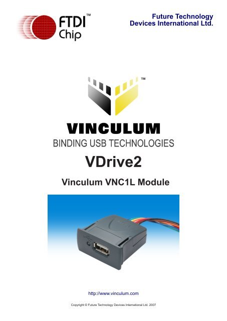
Future TechnologyDevices International Ltd.<strong>VDrive2</strong>Vinculum VNC1L Modulehttp://www.vinculum.comCopyright © Future Technology Devices International Ltd. 2007
1. Introduction and FeaturesPage 1.1 IntroductionThe <strong>VDrive2</strong> module provides an easy solution for adding a USB Flash disk interface to an existing product. Only foursignal lines plus 5V supply and ground are required to be connected. Using the Vinculum VDAP firmware the VNC1L’sI/O interface can be selected between the serial UART or SPI using the on-board jumper pins. Not only is the<strong>VDrive2</strong> ideal for evaluation and development of VNC1L designs, but also its neat enclosure and attractive quantitydiscount structure makes this module suitable for incorporation into finished product designs. The <strong>VDrive2</strong> is ideal forcommercial products such as domestic goods, set top box, etc., as well as industrial products such as data loggers,software upgradable products, etc.The Vinculum VNC1L is the first of F.T.D.I.’s Vinculum family of Embedded SoC USB host controller integrated circuitdevices. Not only is it able to handle the USB Host Interface, and data transfer functions but owing to the inbuilt MCUand embedded Flash memory, Vinculum can encapsulate the USB device classes as well. When interfacing to massstorage devices such as USB Flash drives, Vinculum also transparently handles the FAT file structure communicatingvia UART, SPI or parallel FIFO interfaces via a simple to implement command set. Vinculum provides a new costeffective solution for providing USB Host capability into products that previously did not have the hardware resourcesavailable.1.2 Features• Uses ses F.T.D.I.’s F.T.D.I.s VNC1L emedded embedded host controller I.C. device.• ‘A’ type socket socet to connect Flash disk. dis.• Traffic indicator LED.• 2 mm (0.08”) pitch 8 pin connector.• 8-way header interconnect cable provided.• Only nly four our signals to connect connect excluding ecluding power and ground.• Jumper umper selectable selectale UART T or SPI I interfaces. interaces.• Single ingle 5V V supply input.• Uses Vinc inc VD D firare firar and coand coand set. t.• Enclosure with snap in place clips allows for easy front panel ounting.• rogra or update firare via USB Flash disk or via UART interface.• VNC1L firare prograing control pins ROG# and RESET# brought out onto internal jper interface(only accessible on internal module PC)• <strong>VDrive2</strong> is a Pb-free RoHS complaint development module.• Schatic Schatic and firare firar files fi available avaiab for download donoad fro fro the th Vinculum website.<strong>VDrive2</strong> Vinculum VNC1L Module<strong>Datasheet</strong> Version 0.99 © Future Technology Devices International Ltd. 2007
Page 2. Pin Out2.1 <strong>VDrive2</strong> Pin Out8 RI#Power / Traffic Indicatorbi-colour LED6 CTS#5 TXD4 RXD3 5V02 RTS#1 GNDUSB Flash DriveinterfaceGNDUART/SPI3V3OUTVDRIVE2Figure 1 - <strong>VDrive2</strong> Pin Out - UART interface.Table 1 - Port Selection Jumper PinsUART/SPIPull-UpPull-DownI/O ModeSerial UARTSPI2.2 UART Interface Signal DescriptionsTable 2 - Data and Control us Signal Mode Options - UART InterfacePin No. Name Type Description1 GND PWR Signal ground2 RTS# Output Request To Send Control Output / Handshake signal3 5V0 PWR 5V supply input4 RXD Input Receive asynchronous data input5 TXD Output Transmit asynchronous data output6 CTS# Input Clear To Send Control Input / Handshake signal7 NC - No Connect8 RI# Input Ring Indicator Control Input. Used to resume the Vinculum from suspend.<strong>VDrive2</strong> Vinculum VNC1L Module<strong>Datasheet</strong> Version 0.99 © Future Technology Devices International Ltd. 2007
2.3 SPI Interface Signal Descriptions and Timing DiagramsPage Table 3 - Data and Control us Signal Mode Options - SPI InterfacePin No. Name Type Description5 SCLK Input SPI Clock input 12MHz maximum.4 SDI Input SPI Serial Data Input2 SDO Output SPI Serial Data Output6 CS Input SPI Chip Select InputFigure 2 - SPI Slave Data Read CycleR/W ADDD7D6D5D4D3D2D1D0SPICLKSPI CSSPI Data InSPI Data Out1 1 0StartFrom Start - SPI CS must be held high for the entire read cycle and must be taken low for at least one clock periodafter the read is copleted. The first bit on SI Data In is the R/W bit - inputting a ‘1’ here allows data to be read frothe chip. The next bit is the address bit ADD which is used to indicate whether the data register (‘0’) or the statusregister (‘1’) is read from. During the SPI read cycle a byte of data will start being output on SPI Data Out on the nextclock cycle after the address bit MSB first. After the data has been clocked out of the chip the status of SI DataOut should be checked to see if the data read is new data. A ‘0’ level here on SPI Data Out means that the data readis new data. A ‘1’ indicates that the data read is old data and the read cycle should be repeated to get new data.Remember that CS must be held low for at least one clock period before being taken high again to continue with thenext read or write cycle.StatusFigure 3 - SPI Slave Data Write CycleR/W ADDD7D6D5D4D3D2D1D0SPICLKSPI CSSPI Data InSPI Data Out1 0 0StartStatusFrom Start - SPI CS must be held high for the entire write cycle and must be taken low for at least one clock periodafter the write is copleted. The first bit on SI Data In is the R/W bit - inputting a ‘0’ here allows data to be writtento the chip. The next bit is the address bit ADD which is used to indicate whether the data register (‘0’) or the statusregister (‘1’) is written to. During the SPI write cycle a byte of data can be input to SPI Data In on the next clock cycleafter the address bit MSB first. After the data has been clocked in to the chip the status of SI Data Out should be<strong>VDrive2</strong> Vinculum VNC1L Module<strong>Datasheet</strong> Version 0.99 © Future Technology Devices International Ltd. 2007
Page checked to see if the data read was accepted. A ‘0’ level on SPI Data Out means that the data write was accepted. A‘1’ indicates that the internal buffer is full and the write should be repeated. Remember that CS must be held low for atleast one clock period before being taken high again to continue with the next read or write cycle.Figure 4 - SPI Slave Data Timing DiagramsT1SPICLKT2T3SPICS /SPI DATA INT6T4T5SPI DATA OUTT7Table 4 - SPI Slave Data TimingTime Description Min Typical Max UnitT1 SPICLK Period 83 - - nsT2 SPICLK High 20 - - nsT3 SPICLK Low 20 - - nsT4 Input Setup Time 10 - - nsT5 Input Hold Time 10 - - nsT6 Output Hold Time 2 - - nsT7 Output Valid Time - - 20 nsTable 5 - Status Register (ADD = ‘1’)Bit Description0 RXF#1 TXE#2 -3 -4 RXF IRQEn5 TXE IRQEn6 -7 -<strong>VDrive2</strong> Vinculum VNC1L Module<strong>Datasheet</strong> Version 0.99 © Future Technology Devices International Ltd. 2007
3. VDRIVE2 DimensionsPage Figure 5 - VDRIVE2 chanical dinsions41.29mm /1.63"41.76mm / 1.64"0.44 mm /0.02"2.0 mm /0.08"20.45mm /0.81"17.4 mm /0.69"FrontSideBack7.70 mm /0.30"Vdr ive33.8 mm /1.33"Top2.5 mm /0.10"1.65 mm /0.06"0.70 mm /0.03"Bottom4.20 mm /0.17"Fully detailed mechanical drawings for the <strong>VDrive2</strong> enclosure are available on request from <strong>FTDI</strong> technical support.<strong>VDrive2</strong> Vinculum VNC1L Module<strong>Datasheet</strong> Version 0.99 © Future Technology Devices International Ltd. 2007
Page 4. Application Example - VDRIVE2 to PIC Micro Interface5V05V0+10uFGND5V0100nF10pF20 MHz47kCTS#TXDRXDGNDVDDRA5RA4GNDICSPDATICSPCLKRTS#10pFGNDTXDRXDRTS#MCLR#RXTXRC3RA2RC0RC1RC2CTS#GND47kUSB FlashDriveGNDPIC16F6881uFAC InputVDRIVE2Figure 6 - Datalogging to a Flash disk with the <strong>VDrive2</strong>By adding a IC icrocontroller and a few other coponent the VDRIVE2 odule can be turned into a Flashdisk based data logger. Fig 5 shows the schematic of this simple application. The AC signal input is connected tothe 10-bit analogue to digital converter on board the Microchip IC. The IC code takes a pre-defined nber ofsaples and then writes the corresponding ASCII values to a coa separated value (CSV) file on the USB flashdisk attached to the VDRIVE2 odule. Vinc’s DOS like ASCII coands siplify the task of file handling. Anextended ASCII command set is designed for use with a terminal whilst a shortened hexadecimal version is used witha microcontroller.Consult the Vinc VD firare datasheet for full details of the coand set used by the <strong>VDrive2</strong>.<strong>VDrive2</strong> Vinculum VNC1L Module<strong>Datasheet</strong> Version 0.99 © Future Technology Devices International Ltd. 2007