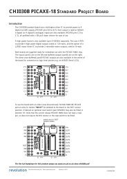
CHI035A PICAXE-18 HIGH POWER BOARD
CHI035A PICAXE-18 HIGH POWER BOARD
CHI035A PICAXE-18 HIGH POWER BOARD

Create successful ePaper yourself
Turn your PDF publications into a flip-book with our unique Google optimized e-Paper software.
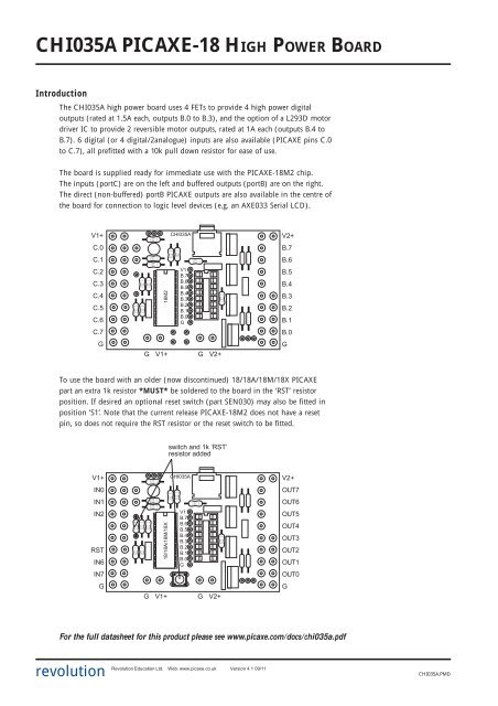
<strong>PICAXE</strong>-<strong>18</strong> <strong>HIGH</strong> <strong>POWER</strong> PROJECT <strong>BOARD</strong>4Output Devices (via FET)Output devices are connected between the pairs of holes on the pcb (pin andV2+) as shown below.<strong>CHI035A</strong><strong>18</strong>M2V1B.7B.6B.5B.4B.3B.2B.1B.0GblackredbuzzerOutput Devices (motors via L293D)The optional L293D chip (part ICO030) may be added to the 16 pin socket onthe board as shown. This then provides forward/backward/halt control of up totwo DC motors. One motor connects to outputs B.4 and B.5, the other to outputsB.6 and B.7<strong>CHI035A</strong><strong>18</strong>M2V1B.7B.6B.5B.4B.3B.2B.1B.0GL293DmotorNote that motors should be suppressedby soldering a 220nF polyester capacitor(part CAP002) across the motor terminalsto prevent electrical noise affecting the circuit.Outputs B.4 & B.5 control one motor, outputs B.6 and B.7 control the other motor.B.4 B.5 motor B.6 B.7 motorlow low halt low low haltlow high forwards low high forwardshigh low backwards high low backwardshigh high halt high high haltrevolution Revolution Education Ltd. Web: www.picaxe.co.uk Version 4.1 09/11 <strong>CHI035A</strong>.PMD
<strong>PICAXE</strong>-<strong>18</strong> <strong>HIGH</strong> <strong>POWER</strong> PROJECT <strong>BOARD</strong>5Input DevicesDigital inputs are connected between V1+ and the input pin as shown below.analoguee.g. potentiometerpulldown resistorsremoved on C.0 & C.1<strong>CHI035A</strong>digitalswitch<strong>18</strong>M2V1B.7B.6B.5B.4B.3B.2B.1B.0GThe connections marked C.3 and C.4 should not generally be used with the<strong>PICAXE</strong> system. These are used by the <strong>PICAXE</strong> chip as the ‘serial in’ and ‘serialout’ PC download connection.All inputs are provided with a 10k pull down resistor pre fitted to the board.However the board is also configured to allow use of inputs C.0 and C.1 asanalogue inputs. Some analogue sensors, such as a potentiometer, will requirethe on-board 10k resistor to be cut off from the positions marked R8 (upperresistor, input C.0) and R7 (lower resistor, input C.1) as shown above.revolution Revolution Education Ltd. Web: www.picaxe.co.uk Version 4.1 09/11 <strong>CHI035A</strong>.PMD
<strong>PICAXE</strong>-<strong>18</strong> <strong>HIGH</strong> <strong>POWER</strong> PROJECT <strong>BOARD</strong>6Connecting to the Project BoardInputs and outputs may be soldered via wires directly to the board. Alternatelyyou may wish to purchase screw terminal blocks (5mm pitch) and solder these tothe boards as shown below. This allows wires to be temporarily connected via thescrew terminals. For one board 6 sets of part CON005 (2x2 pole connector) arerequired.V1+C.0C.1C.2C.3C.4C.5C.6C.7G<strong>18</strong>M2<strong>CHI035A</strong>V1B.7B.6B.5B.4B.3B.2B.1B.0GG V1+ G V2+V2+B.7B.6B.5B.4B.3B.2B.1B.0GNote that when using terminal blocks it is necessary to ‘share’ the V2+ connectorwith all output pins and to ‘share’ the V1+ connector with all inputs. Rememberthat with the FET output buffer the output devices are connected between V2+and the output (NOT output to 0V). Like wise the inputs are connected betweenV1+ and the input.revolution Revolution Education Ltd. Web: www.picaxe.co.uk Version 4.1 09/11 <strong>CHI035A</strong>.PMD
<strong>PICAXE</strong>-<strong>18</strong> <strong>HIGH</strong> <strong>POWER</strong> PROJECT <strong>BOARD</strong>7Appendix A - <strong>CHI035A</strong> Circuit DiagramV+PICV1+C.0C.1C.2C.3C.4C.5C.6C.7GGPICCHI035 Project Board (v4)C1100nR8R7R5R4R2R1All 10k+C2100uCT1RST1knot fittedR1122kR1010k17<strong>18</strong>12315164C.0C.1C.2TxdRcvC.6C.7C.5S1not fitted14IC1<strong>PICAXE</strong><strong>18</strong>M2V+B.713B.612B.511B.410B.39B.28B.17B.060V5R9 (link)RG1 not fittedH0101527In3In4In1In21 9 16 8V+IC20V11Out314Out43Out16Out24 5 12 13D1Q1IRL520RA110kIC2L293DV+PWRV2+B.7B.6B.5B.4B.3B.2B.1B.0GFET & diodecircuit alsorepeated foroutputs 1-3GPWRrevolution Revolution Education Ltd. Web: www.picaxe.co.uk Version 4.1 09/11 <strong>CHI035A</strong>.PMD