Hexaband Planar Inverted-F Antenna With Novel Feed Structure for ...
Hexaband Planar Inverted-F Antenna With Novel Feed Structure for ...
Hexaband Planar Inverted-F Antenna With Novel Feed Structure for ...
- No tags were found...

Create successful ePaper yourself
Turn your PDF publications into a flip-book with our unique Google optimized e-Paper software.
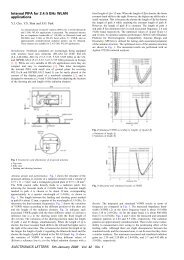
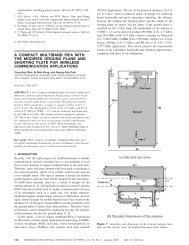
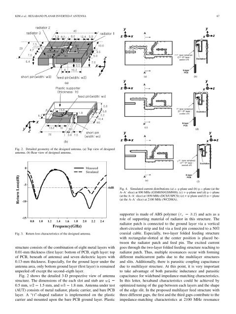
KIM et al.: HEXABAND PLANAR INVERTED-F ANTENNA 67Fig. 2. Detailed geometry of the designed antenna. (a) Top view of designedantenna. (b) Rear view of designed antenna.Fig. 4. Simulated current distributions (a) x-y-plane and (b) y-z-plane (at theA–A slice) at 890 MHz (GSM850/GSM900); (c) x-y-plane and (d) y-z-plane(at the A–A slice) at 1850 MHz (DCS/USPCS); (e) x-y-plane and (f) y-z-plane(at the A–A slice) at 2100 MHz (WCDMA).Fig. 3. Return loss characteristics of the designed antenna.structure consists of the combination of eight metal layers with0.01-mm thickness (first layer: bottom of PCB, eigth layer: topof PCB, beneath of antenna) and seven dielectric layers with0.13-mm thickness. Especially, <strong>for</strong> the ground layer under theantenna area, only bottom ground layer (first layer) is remainedunpeeled off except the second–eigth layer.Fig. 2 shows the detailed 3-D prospective view of antennastructure. The dimensions of the each slot and stub are0.5 mm, 1.5 mm, and 1.8 mm. <strong>Antenna</strong> under test(AUT) consists of metal radiator, plastic carrier, and bare PCBlayer. A “ ”-shaped radiator is implemented on the plasticcarrier and mounted upon the bare PCB ground layer. Plasticsupporter is made of ABS polymerand acts as arole of supporting material of radiator in this structure. Theradiator patch is connected to the ground layer via a verticalshort-circuited strip and fed via a feed pin connected to a 50coaxial cable. Especially, two-layer folded feeding structurewith rectangular-slotted at the center position is placed betweenthe radiator patch and feed pin. The excited currentgoes through the two-layer folded feeding structure reaching toradiator patch. Thus, multiple resonances occur with <strong>for</strong>mingdifferent multicurrent paths due to the multilayer structuresand slits. Additionally, there is parasitic coupling capacitancedue to multilayer structure. At this point, it is very importantto take advantage of both parasitic inductance and parasiticcapacitance <strong>for</strong> wideband impedance-matching characteristics.In this letter, hexaband characteristics could be achieved byoptimized tuning of the gap between each layers and the shapeof the edge slit. In the proposed multilayer feed structure withthree different gaps, the first and the third gaps contribute to theimpedance-matching characteristics at 2100 MHz resonance