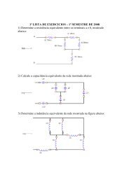
Fundamentals of Microelectronics Chapter 7 CMOS ... - DECOM
Fundamentals of Microelectronics Chapter 7 CMOS ... - DECOM
Fundamentals of Microelectronics Chapter 7 CMOS ... - DECOM

Create successful ePaper yourself
Turn your PDF publications into a flip-book with our unique Google optimized e-Paper software.
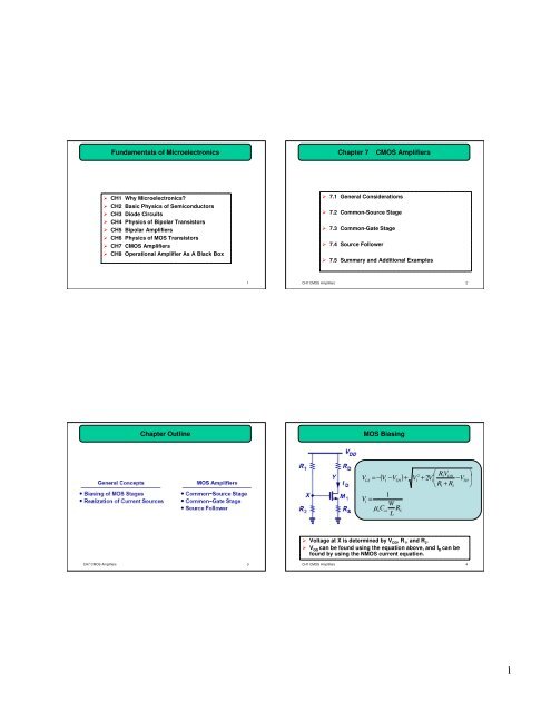
<strong>Fundamentals</strong> <strong>of</strong> <strong>Microelectronics</strong><strong>Chapter</strong> 7 <strong>CMOS</strong> Amplifiers CH1 Why <strong>Microelectronics</strong>? CH2 Basic Physics <strong>of</strong> Semiconductors CH3 Diode Circuits CH4 Physics <strong>of</strong> Bipolar Transistors CH5 Bipolar Amplifiers CH6 Physics <strong>of</strong> MOS Transistors CH7 <strong>CMOS</strong> Amplifiers CH8 Operational Amplifier As A Black Box 7.1 General Considerations 7.2 Common-Source Stage 7.3 Common-Gate Stage 7.4 Source Follower 7.5 Summary and Additional Examples1CH7 <strong>CMOS</strong> Amplifiers 2<strong>Chapter</strong> OutlineMOS BiasingV = −(V −V) +GSTH1V1=WµnCoxRSL12 ⎛ RV2 DD⎞V1+ 2V1⎜−VTH⎟⎝R1+ R2⎠ Voltage at X is determined by V DD , R 1 , and R 2 . V GS can be found using the equation above, and I D can befound by using the NMOS current equation.CH7 <strong>CMOS</strong> Amplifiers 3CH7 <strong>CMOS</strong> Amplifiers 41
Self-Biased MOS StageCurrent SourcesI R + V + R I = VDDGSSDDD The circuit above is analyzed by noting M 1 is in saturationand no potential drop appears across R G .CH7 <strong>CMOS</strong> Amplifiers 5 When in saturation region, a MOSFET behaves as a currentsource. NMOS draws current from a point to ground (sinks current),whereas PMOS draws current from V DD to a point (sourcescurrent).CH7 <strong>CMOS</strong> Amplifiers 6Common-Source StageOperation in SaturationR I < VD DDD−( V −V)GSTHλ = 0A = −gRvA = −vmD2µCnCH7 <strong>CMOS</strong> Amplifiers 7oxWILDRD In order to maintain operation in saturation, V out cannot fallbelow V in by more than one threshold voltage. The condition above ensures operation in saturation.CH7 <strong>CMOS</strong> Amplifiers 82
CS Stage with λ=0CS Stage with λ ≠ 0A = −gRRRvinout= ∞= RmLLA = −gRRvinout= ∞( R || r ) However, Early effect and channel length modulation affectCE and CS stages in a similar manner.mLL= R || rOO9CH7 <strong>CMOS</strong> Amplifiers 10CS Gain Variation with Channel LengthCS Stage with Current-Source LoadA =vW2µnCoxL ∝λ I Since λ is inversely proportional to L, the voltage gainactually becomes proportional to the square root <strong>of</strong> L.D2µnCoxWLICH7 <strong>CMOS</strong> Amplifiers 11DA = −gRvout= rm1O1( r || r )|| rO1O2O2 To alleviate the headroom problem, an active currentsourceload is used. This is advantageous because a current-source has a highoutput resistance and can tolerate a small voltage dropacross it.CH7 <strong>CMOS</strong> Amplifiers 123
PMOS CS Stage with NMOS as LoadCS Stage with Diode-Connected LoadA = −gv( rO1||r2)m2 O Similarly, with PMOS as input stage and NMOS as the load,the voltage gain is the same as before.CH7 <strong>CMOS</strong> Amplifiers 13A =−gvA =−gvm1m11⋅gm2( W/L)1=−( W/L)⎛ 1⎜ || rO2|| r⎝gm2 Lower gain, but less dependent on process parameters.CH7 <strong>CMOS</strong> Amplifiers 14O1⎞⎟⎠2CS Stage with Diode-Connected PMOS DeviceCS Stage with Degeneration⎛ 1 ⎞A = −g⎜ || r || r ⎟v m2 o1o2⎝ gm1⎠ Note that PMOS circuit symbol is usually drawn with thesource on top <strong>of</strong> the drain.15RDAv=−1+ RSgλ = 0m Similar to bipolar counterpart, when a CS stage isdegenerated, its gain, I/O impedances, and linearity change.CH7 <strong>CMOS</strong> Amplifiers 164
Example <strong>of</strong> CS Stage with DegenerationCS Stage with Gate ResistanceVRG= 0RDAv= −1 1+g gm1m2 A diode-connected device degenerates a CS stage.CH7 <strong>CMOS</strong> Amplifiers 17 Since at low frequencies, the gate conducts no current,gate resistance does not affect the gain or I/O impedances.CH7 <strong>CMOS</strong> Amplifiers 18Output Impedance <strong>of</strong> CS Stage with DegenerationOutput Impedance Example (I)r ≈ g r R + routm OSO⎛ 1 ⎞ 1Rout = rO1⎜1+ g ⎟+⎝ g ⎠ gm1m2m2 Similar to the bipolar counterpart, degeneration boostsoutput impedance.CH7 <strong>CMOS</strong> Amplifiers 19 When 1/g m2 is parallel with r O2 , we <strong>of</strong>ten just consider 1/g m2 .CH7 <strong>CMOS</strong> Amplifiers 205
Output Impedance Example (II)CS Core with Biasingout( g m 1rO 21) r O 1R ≈ + In this example, the impedance that degenerates the CSstage is r O , instead <strong>of</strong> 1/g m in the previous example.CH7 <strong>CMOS</strong> Amplifiers 21R1|| R2−RDR1|| R2Av= ⋅ , Av= − gmRRG+ R1|| R 12+ RRG+ R1|| R2Sgm Degeneration is used to stabilize bias point, and a bypasscapacitor can be used to obtain a larger small-signalvoltage gain at the frequency <strong>of</strong> interest.CH7 <strong>CMOS</strong> Amplifiers 22DCommon-Gate StageSignal Levels in CG StageA = g RvmD Common-gate stage is similar to common-base stage: arise in input causes a rise in output. So the gain is positive.CH7 <strong>CMOS</strong> Amplifiers 23 In order to maintain M 1 in saturation, the signal swing atV out cannot fall below V b -V TH .CH7 <strong>CMOS</strong> Amplifiers 246
I/O Impedances <strong>of</strong> CG StageCG Stage with Source Resistance1Rin=gλ = 0mRout= R Dvoutvout( 1/ gm)RD= gmRD⇒ =gmRD=1/ gMvvin( 1/ gm) + R 1Sin+ RS1/ g + RgmSm The input and output impedances <strong>of</strong> CG stage are similarto those <strong>of</strong> CB stage.CH7 <strong>CMOS</strong> Amplifiers 25 When a source resistance is present, the voltage gain isequal to that <strong>of</strong> a CS stage with degeneration, only positive.CH7 <strong>CMOS</strong> Amplifiers 26Generalized CG BehaviorExample <strong>of</strong> CG Stage( )ORout= 1 + gmrORS+ r When a gate resistance is present it does not affect the gainand I/O impedances since there is no potential drop acrossit ( at low frequencies). The output impedance <strong>of</strong> a CG stage with source resistanceis identical to that <strong>of</strong> CS stage with degeneration.CH7 <strong>CMOS</strong> Amplifiers 27vvoutinVXVin=gm11//g m11//gm21+ RSgm2gm1R=1 + ( g m 1+ gDm 2) R S11=RS( gm1 + gm2) + 1⎡ ⎛ 1 ⎞ ⎤Rout≈ ⎢gm1rO1⎜|| RS⎟+ rO1|| Rg⎥⎣ ⎝ m2⎠ ⎦ Diode-connected M 2 acts as a resistor to provide the biascurrent.CH7 <strong>CMOS</strong> Amplifiers 28D7
CG Stage with BiasingSource Follower StagevoutR=v R ||in33||( 1/ gm)( 1/ g ) +m⋅gRRGm DAv
Output Resistance <strong>of</strong> Source FollowerSource Follower with Biasing1 WI( ) 2D= µnCoxVDD−IDRS−VTH2 L1 1Rout= || rO|| RL≈ || RLg gm The output impedance <strong>of</strong> a source follower is relatively low,whereas the input impedance is infinite ( at lowfrequencies); thus, a good candidate as a buffer.CH7 <strong>CMOS</strong> Amplifiers 33m R G sets the gate voltage to V DD , whereas R S sets the draincurrent. The quadratic equation above can be solved for I D .CH7 <strong>CMOS</strong> Amplifiers 34Supply-Independent BiasingExample <strong>of</strong> a CS Stage (I) If R s is replaced by a current source, drain current I Dbecomes independent <strong>of</strong> supply voltage.CH7 <strong>CMOS</strong> Amplifiers 35⎛ 1⎞Av= − gm 1⎜|| rO1|| rO2|| rO3⎟⎝ gm 3⎠1Rout= || rO1|| rO2|| rO3gm 3 M 1 acts as the input device and M 2 , M 3 as the load.CH7 <strong>CMOS</strong> Amplifiers 369
Example <strong>of</strong> a CS Stage (II)Examples <strong>of</strong> CS and CG StagesrO2Av=−1 1+ || rg gm1 M 1 acts as the input device, M 3 as the source resistance,and M 2 as the load.CH7 <strong>CMOS</strong> Amplifiers 37m3O3[( 1+gm2rO2)RSrO2] rO1A +v_ CS= −gm1||r // rO2=+ RSgO1v_ CG1m2 With the input connected to different locations, the twocircuits, although identical in other aspects, behavedifferently.CH7 <strong>CMOS</strong> Amplifiers 38AExample <strong>of</strong> a Composite Stage (I)Example <strong>of</strong> a Composite Stage (II)RDAv=1 1+g gm1m2 By replacing the left side with a Thevenin equivalent, andrecognizing the right side is actually a CG stage, thevoltage gain can be easily obtained.CH7 <strong>CMOS</strong> Amplifiers 39vvout21|| rgm3= −1|| rgm2O3O2|| r This example shows that by probing different places in acircuit, different types <strong>of</strong> output can be obtained. V out1 is a result <strong>of</strong> M 1 acting as a source follower whereasV out2 is a result <strong>of</strong> M 1 acting as a CS stage withdegeneration.CH7 <strong>CMOS</strong> Amplifiers 40inO41+gm110