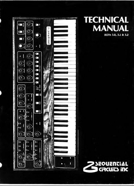
Sequential Circuits Prophet-5 Service Manual - Audiofanzine
Sequential Circuits Prophet-5 Service Manual - Audiofanzine
Sequential Circuits Prophet-5 Service Manual - Audiofanzine

Create successful ePaper yourself
Turn your PDF publications into a flip-book with our unique Google optimized e-Paper software.
^^. ^ ^s .y ^,-j?^ ^^w^-^>&i^^^V^?v-^ftf*^«^i^«.?^«^>^>^4^?ipe^^iSH^^;*I .,f^S-y^.^"^^^^^4^"v-^1 Hj^ 7>W+^^^^ Arl'^'\^i *' .^f ^.'^^^'*I.ftJ^^^^T^'-^'^'^' " "^^^^' ""^"'^^VJ-^'^v:^V^-->^^"- Lt-Jixw t A-ViT-" Vl^'r.r*!uU^^if1*^t^'^-T -^i>tJ^V > rt*^^C^vSh^ -•^ ^ -^^\>rt \ _nvf-'1J^.-^,:^^^ rr— '-A-^H_ ^f^,^7-«n?T>TnK^-i^l^ i' t^\ni\>\\ .^.&
MODEL 1000S/N 1301 and AboveRevisions 3.0, 3.1 and 3.2<strong>Manual</strong> No. TM1000D.2SYNTHESIZERTECHNICAL MANUALSECOND EDITIONBy STANLEY jUNGLEIBWine Country Productions. Inc.1572 Park Crest Court, Suite #505San Jose, California 95118 USAPhone: (408) 265-2008 FAX (408) 266-6591SEQUENTIAL Product Speciafists Since 1987I
PROPHET-5 SYNTHESIZERTECHNICAL MANUALBy Stanley JungleibArtwork: Denis SimardGreg ArmbrusterSecond EditionFor Revisions 3.0, 3.1 and 3.2<strong>Manual</strong> No. TM1000D.2Issued: October, 1981Copyright0i981 bySEQUENTIAL CIRCUITS, INC.All rights reserved. Printed in USA.The contents of this manual are the propertyof SCI and are not to be copied or reproducedwithout our prior written permission.D.2
'1^iAbout This <strong>Manual</strong> and Servicing The <strong>Prophet</strong>The <strong>Prophet</strong> is a sophisticated instrument and SCI issues its technical manual for use by qualifiedtechnicians only. Of course the manual will be read by <strong>Prophet</strong> owners and others interested insynthesizer design. And we realize it will also be used by some to develop modifications for theinstrument. While we support this innovative attitude in spirit, we cannot support it financially:Modifications or unauthorized service void the <strong>Prophet</strong>'s warranty. They also invariably extend servicetime (thus, cost) if factory repair is required. Familiarize yourself thoroughly with this manual beforeattempting any work on the <strong>Prophet</strong>. This will at least help you judge whether you should be workingon it at all. If in doubt, please contact our <strong>Service</strong> Department.This edition of the Technical <strong>Manual</strong> (TM1000D) documents <strong>Prophet</strong>-5s with serialnumbers 1301 andabove. Although great care was taken to ensure the changes would be transparent to players,predecessors. Rev 2 (S/N 184-1299, seetechnicians will find "Rev 3" quite a different instrument from itsTM1000C) was a mere refinement of Rev 1 (S/N 1-182). Rev 3, however, uses new voltage-controlled ICsin the analog synthesizer and, in the microcomputer, a vastly different ADC, DAC and control voltagedistribution scheme. Although the main purpose of the revision was to remove production limitationscaused by inconsistent supply and quality of the previous synth *'chip set/' the hardware redesignencouraged the implementation of more sophisticated editing, tuning and maintenance software whileimproving servicabiiity; the number of voice trimmers being reduced from 80 to 45.The manual is organized as follows:SECTION 1, MECHANICAL provides a physical introduction and directions fordisassembling/assembling the <strong>Prophet</strong>.SECTION 2, THEORY explains general function and circuit operation, referring to block diagrams and tothe schematics for hardware details.SECTION 3, DOCUMENTS contains schematics and pictorials identifying all components.SECTION 4, SERVICE contains procedures for routine tests and trims.SECTION 5, PARTS cross-references component designators to SCI stock numbers.SECTION 6, GLOSSARY decodes abbreviations appearing on SCI documentation.SECTION 7, APPENDIX contains selected data sheets.Your response to the questionnaire on the next page will help us monitor our publication's usefulnessAbout The Second EditionIn addition, to the original revision 3.0 data (with a few corrections), the followingmaterial covering later refinements of the instrument has been added. The revisionsoccured chiefly in the microcomputer's memory configuration, added PITCH and MODCV inputs, and in the addition of a serial interface for communication with the Model1005 Polyphonic Sequencer or Model 1001 Remote Keyboard.SECTION if THEORY discusses the hardware changes comprising revisions 3.1 and 3.2.SECTION 9, PROGRAMMING covers use of the serial interface.mSECTION 10, DOCUMENTS contains schematics and pictorials for revisions 3.1 and 3.2.SECTION 11, SERVICE includes instructions for updating a 3.0 or 3.1 instrument tolevel 3.2, for using the diagnostic memory tests, and for an added adjustment onPCB 3.SECTION 12, PARTS lists SCI stock numbers for 3.1 and 3.2-Ievel assemblies.D.2
iJTable of ContentsISECTION 1MECHANICAL1-0 GENERAL 1-11-1 PRECAUTIONS 1-11-2 SERVICE POSITION 1-11-3 PCB 4 VOICE BOARD 1-31-4 PCB 3 COMPUTER BOARD 1-41-5 PCB 1/2 CONTROL PANELS 1-51-6 KEYBOARD 1-6SECTION 2THEORY2-0 GENERAL 2-12-1 SYNTHESIZER BACKGROUND 2-12-2 THE PROPHET 2-42-3 ANALOG SYNTHESIZER DESCRIPTION 2-72-4 OSCILLATOR A, B AND LFO 2-82-5 MIXER AND AMOUNT VCAS 2-92-6 FILTER 2-92-7 ENVELOPE GENERATORS 2-92-8 AUDIO OUTPUT 2-102-9 MICROCOMPUTER SYSTEM DESCRIPTION 2-102-10 MICROPROCESSOR, MEMORY, AND I/O INTERFACE 2-122-11 CONTROL MATRICES 2-152-12 ADC, DAC, AND CV OUTPUTS 2-162-13 TUNE AND A-440 2-192-14 SEQUENCER INTERFACE 2-202-15 CASSETTE INTERFACE 2-21SECTIONSDOCUMENTS3-0 DOCUMENT LIST 3-13-1 DOCUMENT NOTES 3-1SECTION 4SERVICE4-0 GENERAL 4-14-1 OSCILLATOR A TEST 4-34-2 OSCILLATOR B TEST 4-44-3 MIXER AND NOISE TEST 4-54-4 UNISON AND GLIDE TEST 4-54-5 FILTER TEST 4-64-6 AMPLIFIER TEST 4-64-7 LFO AND WHEEL-MOD TEST 4-74-8 POLY-MOD TEST 4-84-9 FINAL TEST 4-94-10 POWER SUPPLY TRIM 4-104-11 PITCH WHEEL TRIM 4-104-12 MASTER SUMMER OFFSET TRIM 4-104-13 WHEEL-MOD LFO VGA BALANCE 4-104-14 DAC GAIN, ADC GAIN, SEQ INTERFACE TRIM 4-114-15 WHEEL-MOD NOISE VGA BALANCE 4-114-16 VCO SCALE TRIM 4-124-17 POLY-MOD FILTER ENVELOPE VGA BALANCE 4-134-18 POLY-MOD OSCILLATOR B VGA BALANCE 4-134-19 FILTER ENVELOPE AMOUNT VGA BALANCE 4-144-20 FILTER TUNING 4-144-21 FINAL VCA BALANCE 4-164-22 VOICE VOLUME 4-16
1SECTION 5PARTS5-05-15-25-35-45-55-6CHASSIS 5-1PCBPCB 2 5.1PCB 3 ...........5-2PCB 4 5.4PCS 5s-^'.'.'.'.'.'.'.'.'.'.'.'.'.'.'.'.'.'.'.5-8BILL OF MATERIALS (TOTAL ITEMS) 5-9SECTION 6GLOSSARYSECTION 7APPENDIXCA3280 Dual Operational Transconductance AmplifierCEM 3310 Voltage Controlled Envelope GeneratorCEM 3320 Voltage Controlled FilterCEM 3340/3345 Voltage Controlled OscillatorSECTION 8THEORY8-0 INTRODUCTION8-1 REVISION 3.1 COMPUTER and POWER SUPPLY8-2 REVISION 3.2 COMPUTER and USART8-3 REVISION 3.2 ANALOG and POWER SUPPLY8-18-18-28-^SECTION 9PROGRAMMING9-0 INTRODUCTION9-1 Data Format9-2 Error Checking9-3 Status Bytes9-«f STATUS 0: SEND KEYBOARD and PROGRAM9-5 STATUS 1: ACK, RECEIVE KEYBOARD and PROGRAM9-6 STATUS 2: TRANSPOSE ON9-7 STATUS 3: SAVE TO TAPE9-8 STATUS U: LOAD FROM TAPE9-9 STATUS 5: CLEAR TRANSPOSE9-10 STATUS 6: INITIALIZE SEQ LOWER PROGRAM9^11 STATUS 9: DISABLE TUNE9-12 STATUS A: ENABLE TUNE9-13 STATUS B: RECEIVE PROGRAM CHANGE9-1^* STATUS C: SYSTEM CONNECT9-15 STATUS E: RECEIVE SHORT KEYBOARD DATA9-19-19-29-29-39-39-59-59-69-69-69-69-69-6SECTION 10DOCUMENTS10-0 DOCUMENT LIST10-1SECTION 11SERVICE1 1-0 INTRODUCTION11-1 REVISION 3.2 RETROFIT KIT INSTRUCTIONS11-2 REVISION 3.0 MEMORY TEST11-3 REVISION 3.1 MEMORY TESTll-'f REVISION 3.2 MEMORY TEST11-5 WHEEL-MOD BALANCE TRIM11-111-111-511-6SECTION 12PARTSREVISION 3.2 COMPONENTS
'1SECTION 1MECHANICAL1-0 GENERALThis section shows how to remove the <strong>Prophet</strong>'s main assemblies. Not all of the procedures given hereshould be necessary at any one time. For some service situations you will only need to separate the topand bottom panel assemblies and arrange them as shown in Figure 1-0. This configuration, discussed inparagraph 1-2, allows access to ail trimmers on PCB 4 and most trimmers on RGB 3. However, for someRGB 3 trims you will have to swing-out or completely remove PCB 4, as discussed in paragraph 1-3.1-1 PRECAUTIONSObserve the following precautions when working on the <strong>Prophet</strong>:SWITGH POWER OFF AND GHEGK 115/230V SWITGH ON BAGK PANEL BEFORE GONNECTINGPROPHET TO ROWER OUTLET OR AMPLIFIER.NEVER TOGGLE 115/230V SWITGH WITH POWER ON,TRIMMING, OF GOUR5E, MUST BE PERFORMED WITH ROWER ON. SO AVOID THE POWER SUPPLYPRIMARY GIRGUITRY, WHIGH GONDUGTS LETHAL VOLTAGE.SWITGH POWER OFF BEFORE DISCONNECTING OR CONNECTING ANY CIRCUITRY, ORREMOVING OR INSTALLING RGBs.IMPORTANT! WHENEVER THE AUDIO GABLE IS DISCONNECTED, RGB 3 MUST BE GROUNDED TOTHE BACK RACK PANEL.DO NOT BEND OR STRAIN THE RGBs, OTHERWISE MAY CAUSE TINY BREAKS IN THE PRINTED-CIRCUIT TRACES WHICH WILL BE EXTREMELY DIFFICULT TO FIND.TO REPLACE SOLDERED COMPONENTS SWITCH POWER OFF, REMOVE THE PCB COMPLETELYFROM THE INSTRUMENT AND DESOLDER FROM BOTH SIDES. USE A VACUUM SYRINGE OR DIPDESOLDERER. KEEP VACUUM SYRINGES CLEAN TO PREVENT THEM FROM SPRAYING MOLTENSOLDER. DON'T OVERHEAT THE PADS. WORK CAREFULLY!1-2 SERVICE POSITIONTO PREVENT DAMAGE TO THE TOP PANEL, KEYBOARD, OR WOODWORK, USE A CARPETTED ORSIMILARLY-COVERED WORK SURFACE WHEN OPENING THE BOX.To5et up the <strong>Prophet</strong> for service first switch power off, unplug power cord, and turn instrument over toexpose bottom panel. Remove two large screws near front feet. Remove eleven screws aroundperimeter of bottom panel.Holding top and bottom panel assemblies together, turn the <strong>Prophet</strong> right-side-up again. Remove fourscrews along top edge of back panel. Slowly slide the top panel assembly forward—about nine inches—so when raised the control pane! will clear the large power supply capacitors.1-1
TOPPANELASSEMBLYPCB3COMPUTEROSCILLATOR ANDFILTER CVDEMULTIPLEXERSAMPLE/HOLDSPCB4VOICESZ-80CPUNON-VOLATILEPROGRAM RAMVOICE 1VOICE 2EPROMVOICE 3SCRATCHPADRAMVOICE 4VOICE 5BOTTOMPANELASSEMBLYFINALVCAsMEMORY ANDI/O INTERFACELATCHESCOMMON ANDPATCH CVDEMU^riPLEXERSAMPLE/HOLDSP303/VOICEPOWERCABLEENVELOPEW2GENERATORSPCB 3/4INTERCONNECTPOLY-MOD/FILTERENVELOPEVCAsPOLY-MODOSCBVCAsAUDIO3OUTPUTMIXER P402/AUDIOOUTPUTCABLEFigure 1-0SERVICE POSITION
Raise the top panel assembly to service position shown. For best stability both top panel side back edgesshould rest on the bottom panel. Actually, the top panel upper edge rests on the back panel cable. Thisisnormal; but a small (half-inch) prop may be added to improve stability.The instrument can operate normally in this position. Of course its operating temperature will be farbelow normal. This may slightly affect adjustments or the performance of certain ICs.IREMEMBER THAT IN SERVICE POSITION THE TOP PANEL ASSEMBLY BALANCES ON ITS REAR EDGES.DONT UPSET THIS BALANCE BY PUSHING TOO HARD WHEN PROBING OR TRIMMING.When reassembling the <strong>Prophet</strong>, turn instrument over and firststart two large screws near front feet.Then start bottom and back panel screws to obtain overall alignment before tightening all screws.1-3 PCB 4 VOICE BOARDPCB 4 may be swung-out and operated under power. For this set-up, switch power off, remove screwsidentified in Figure 1-0 in the order suggested, and position board on insulation as shown in Figure 1-1.^-^^jv.^^^^^•^^-.•^ ^^. ^Figure 1-1PCB 4 SWINCOUTINSULATIONCOMMONANALOGTO PREVENT.GROUND LOOPS, PCB 3 IS GROUNDED ONLY THROUGHTHE AUDIO CABLE TO THEBACK PANEL. THEREFORE, WHENEVER THE AUDIO CABLE iS DISCONNECTED, PCB 3 MUST BE TIEDTO THE BACK PANELCAREFUL! DONT ALLOW PCB 4 TO SHORT AGAINST STANDOFFS FROM PCB 3 OR AGAINST THEBOTTOM PANEL.To remove W2, completely switch power off and disconnect voice power cable at P303 on PCB 3 (seeFigure 1-0). Also remove PCB 3/4 interconnect at P401 on PCB4, with a gentle "see-saw" motion. Detachaudio output cable from P402.When reconnecting voice power and audio output cables, be sure tabs interlock. Also be sure the PCB3/4 interconnect is correctly mated and firmly seated at P304 and P401.1-3Lri
1-4 PCB 3 COMPUTER BOARDPCB 3 is held by the screws identified in Figure 1-2, and by two direct connectors to PCB 2, behind it. Toremove PCB 3 first remove PCB 4.remove screws, and pull while rocking the board to minimize stress.Disconnect back panel cable from P302 and wheel cable from P301^P301/WHEELCABLE 5PANELCABLEFigure 1-2PCB 3 MOUNTINGWhen replacing be sure allAlignment isconnector pins are correctly mated with PCB 2 before fastening screws.insured by machine screw holes with their standoffs. Remember to reconnect the wheelcable, too, before replacing PCB 4.interlock.When reconnecting wheel and back-panel cables, be sure tabs1-4
1-5 PCB 1/2 CONTROL PANELSOnce PCB 3 and PCB 4 have been removed, control pane! removal involves pulling off all knobs,unscrewing all potentiometer mounting nuts—using a half-inch nutdriver—and removing screwsidentified in Figure 1-3.J201/W1KEYBOARDCABLEPCB 2LEFTCONTROLPANELW201PCB 1/2INTERCONNECTFCB1RIGHTCONTROLPANELFigure 1-3PCB 1/2 MOUNTINGWhen replacing, check keyboard cable, that ail pots fit correctly through the front panel, and thatswitches operate freely before tightening pot nuts.v;^f'1-5
1-6 KEYBOARDAfter removing PCB 3 and PCB 4, turn the top panel assembly over and disconnect keyboard cable atj201 (see Figure 1-3).Figure 1-4 details keyboard mounting. At both ends, remove keybed supports by first removing keybedscrews then rear keyboard mounting screws.keyboard will slide out of the case—and back in—as shown in Figure 1-5.Remove front keyboard mounting screws. The entireCAREFUL! DURING THIS OPERATION THE J-WIRES FOR THE LOWEST AND HIGHEST KEYS AREVULNERABLE TO DAMAGE FROM COLLISION WITH THE KEYBOARD MOUNTING BRACKETS.WHEN REPLACING CHECK J-WIRES AT EACH END OF KEYBOARD FOR CONTACT WITH BUS BAR.Also, remember to attach the wheel ground lug.R1PITCHWHEELPITCHWHEELDETENTSHAFTSLOTR2MODWHEELFRONTKEYBOARDMOUNTINGSCREWJ-WIRESBUSBARSETSCREWWHEELGROUNDLUGREARKEYBOARDMOUNTINGSCREWKEYBEDSCREWKEYBEDSUPPORTKEYBOARDMOUNTINGBRACKETFigure 1-4KEYBOARD MOUNTING1-6
Figure 1-5KEYBOARD REMOVAL1 -7/1 -8
SECTION 2THEORY2-0 GENERALThis section explains the <strong>Prophet</strong>'s theory of operation. First a general description relates the <strong>Prophet</strong> tothe basic analog synthesizer and introduces the concepts central to the <strong>Prophet</strong>'s advances overconventional performance instruments; programmability and polyphony. Then the analog synth andmicrocomputer functions are covered and their sub-circuits detailed. Throughout it is assumed thereader is already familiar with <strong>Prophet</strong>-5 operation (see Operation <strong>Manual</strong> CM1000B).2-1 SYNTHESIZER BACKGROUNDThe synthesizer is a new instrument but the urge to set technology in search of music is quite old.Consider the pipe organ; of traditional instruments, most like the synthesizer. The organ achieved itsbroad dynamic, pitch and timbral ranges through intricate mechanical arrays; for generating steadywind, transferring key action to pneumatic valves for each note, activating ranks of pipes, and to couplepedalboards and keyboards. Later, the bellows tremolo and pedal-operated swell shutters were addedfor dynamic and timbral expression. As the organ expanded into larger halls pneumatic and hydraulicdevices were developed to Isolate the keyboard from the force required to key more pipes at higherwind pressure. With the advent of electricity the keyboard and drawknobs, formerly levers, becameswitches.Elaborate relay banks now drove solenoid valves for each pipe. More recently, electronicorgans— in many variations—have relied on motor-driven tone generators or switch/relay banks foroscillator frequency division or waveform addition or shaping. Another influential technology, the taperecorder captured natural, instrumental, and electronic sounds for new uses and stimulated the idea ofcomposing music not performable "in real time" on conventional Instruments. A few keyboardinstruments have been directly based on tape mechanisms.Now, what is a synthesizer? It can be distinguished from the organ or tape recorder by reliance onelectronic rather than mechanical devices to generate and modify sound. Except for performer'scontrols a synth need have no moving parts. (Even this exception may one day disappear.) Thus it is farmore flexible and controllable than an organ. In contrast to organ or tape technology, voltage control(VC) allows the immediate and precise adjustment of the basic parameters of an audio stage such asoscillator (VCO) or filter(VCF) frequency, or amplifier (VGA) gain, by a signal from another VCO, anenvelope generator (ENV GEN), keyboard (KBD) or sequencer (SEQ). Most music isanalyzable intoelements replicable by a few VC-modules. For example, if a synth imitates a drum or piano it is not bybeing a (mechanical) percussion instrument, but by simulating the dynamic envelope accompanyingpercussive sounds with a VGA under control of an ENV GEN.2-1'h
TOADDITIONALVCOsTOADDITIONALENV GENsADDITIONALHARMONICS
440 HzAw, 440 Hz^ "OBOE"KBD CVENV GEN® ® (D ®ENV GEN® ® © eg)GATE/TRIGFigure 2-1MONOPHONIC SUBTRACTIVE SYNTHESISBesides a dynamic envelope a musical voice usually has a pitch and timbre which consists of afundamental and a number of harmonic frequencies—all of varying relative strengths. Pitch and timbresynthesis raises a distinction between two techniques, diagrammed in Figures 2-0 and 2-1. The firsttechnique, additive synthesis, might create a timbre by summing the output of several sine-wave VCOsfor the fundamental and each harmonic. In contrast, subtractlve synthesis can start with one sawtoothwaveVCO generating the fundamental with extensive harmonics, then obtain the desired timbre bysubtracting unwanted harmonics with a low-pass VCF.The additive and subtractive techniques have encouraged the development of two types of instruments,roughly, "studio" and "performance." Actually most organs use additive synthesis, but since with asynth one can individually control the level of each harmonic over time additive synthesis may bepotentially more accurate for synthesizing a particular sound. Whether additive or subtractive, studiosynths may be configured from dozens of modules interconnected by patch cords. The modules haveknobs to establish the initial settings of VC-parameters such as initial frequency (FREQ), pulse width(PW), and resonance (RES). But the flexibility and complexity of modular synths has discouraged theirlive use on stage because significant sound changes often require repatching modules and preciselychecking knobs. Favorite, complex sounds take a long-time to create, and almost as long to recreate on amodular synth. So these monophonic (one-voice) synths instead feed multi-track recorders on whichpolyphonic interpretations or compositions are actually orchestrated.A comparison of the number of modules and interconnections depicted In Figures 2-0 and 2-1 showswhy the subtractive configuration has become the popular technique for performance synths.Subtractive synths may be smaller, so, more portable. Their patches will not be as elaborate, so, easier tochange. Originally, performance synths were monophonic. Or they exploited organ technology somore than one note could be played at a time. "Preset" switches that select fixed patches supplantedmany modular controls. Though one could certainlychange sounds quickly by using them, manyplayers have found preset synths unsatisfactory because they eliminate an essential part of synthmusicianship—control of the sound itself.Some manufacturers have offered partially-programmableinstruments. But before the <strong>Prophet</strong> appeared it was not possible for a keyboardist to instantly select hisor her own customized synth sounds and play them polyphonically.2-3
2-2 THE PROPHETThe <strong>Prophet</strong> is a subtractive, analog synthesizer suitable for performance or studio use. It providesinstantaneous patch repeatability and polyphonic capability without the limitations of organ technologyor fixed presets. The term "digital-analog hybrid" is often used to describe the <strong>Prophet</strong>. It means thedigital computer controls the analog audio sources and modifiers. The computer itself generates nosound (except for the A-440 reference).Figure 2-2 diagrams the <strong>Prophet</strong> at the most general level. Instead of controlling the synth directly, thekeyboard and most controls are processed through a microcomputer system. The system provides a wayto store all of the switch and knob settings which form a patch, and solves the problem of generatingfive sets of oscillator (OSC) and filter (FILT) CVs and GATEs from a single keyboard. The Common Analogcircuitry mixes the few non-processed controls with processed signals for the voices. Although only onevoice is depicted on the control panel, the black knobs and switches patch the five voices identically.This makes the voices homophonous—they sound alike—with pitch differences corresponding to (atmost) five simultaneously-held keys.DIGITALANALOGCOMMONANALOG/7\CONTROL PANEL/KEYBOARDMICROCOMPUTER; 7 SYSTEM^ \^ li75 -VOICESYNTHFigure 2-2PROPHET GENERAL BLOCK DIAGRAMFigure 2-3 shows the principle funaions of the four main blocks. Beginning with AUDIO OUT, the voiceoutputs are combined and overall volume set by the VOL VCA controlled directly from the controlpanel. Each voice isa complete synthesizer with two VCOs, a MIXER, VCF, FINAL VCA, and two ENVGENs. Each of the ten VCOs has its own FREQ CV, which allows the computer to individually fine-tunethem and allows the voices to follow separate keys. Each voice receives its own GATE, which triggers thetwo envelope generators with each keystroke.Allswitch commands and most CVs are generated by the computer. Non-processed CVs includeMASTER TUNE, PITCH-bend, and WHEEL-MODulation which are mixed in the Common Analogcircuitry. The Common Analog circuitry also requires a few switch commands.The microcomputer performs the task of voice assignment. It decides which held keys sound whichvoices through the OSC and FILT CVs and GATEs. Voice 1 is assigned to the first key hit. Voice 2 to thesecond key, and so on. After the five initial assignments the system is"last note priority." The earliestusedvoice isreassigned to each new note played. Repeated notes key the same voice. For example,holding C, D, E, F, and G, sustains Voices 1, 2, 3, A, 5, respectively. Adding A "steals" Voice 1C-key, whose pitch disappears even though the key may stillbe held.from the2-4
Figure 2-3PROPHET FUNCTIONAL BLOCK DIAGRAM
COMMON ANALOGVOICE(VOiCES e-5 ARE SfMiLAR)U427-> TO OTHER \/OlCE FfL TERSRI04MTUN^^^ TBia/2a7U370MTUN/P9N0U410OSC lA 5/H 0~K>\/U454WHITE NOISE SOURCENOISE CVMIX NSEVCANOISEFROM COMPUTERA-440VOICESPiTCH-I5Vi/f2 P30!D3fS-TUNE«L/£?£"t/JTC?U379U371OSC A PWA SUM CVPW A SUMPC83 PCB4OSC IASYNCU446AA1rU4594016Close,^A4016close Ail^OSC ALOW-PASS VCFU469IN 3320 OUTRC5QFREQ CV3280VOICE 4\^fCE 3.U477 WCE215 VOICE IR4S29VOLAuo/0 ourU479 [^48/- 5534>-4>»> f04NV"CCONVy^ r-|>2>]JOUT AUDOOUTBFRJfUGLIDE CV O'iOV^n^ ajna.620 J CMUNI CV 0-5/U37SWHEEL-MODGLIDE OUT 0'5VU379lOSCBKBDWMOD PW AJJ373TL08Z.U37I +'?^ U37I1005C B LQMSUMU409^^^7 OSCIBS/H J-£VB SUM CVPW BCVPC83\PCB
OSC B KBD and FILT KBD switches are for keyboard tracking in UNISON mode. UNISON CV is^.In UNISON (monophonic) mode a UNISON CV derived from the lowest note played on the keyboardbecomes the main pitch controi for allvoices through the Common Analog circuitry. The five GATEsoccur simultaneously, but the envelope generators only re-trigger ifno keys are held.The microcomputer system itself consists of the microprocessor or CPU, memory (MEM), andinput/output (I/O) Interface. The CPU executes the program permanently residing in the read-onlymemory (EPROM). This program determines how the various input devices— keyboards, switches, andknobs—are "read", and how "data" generated by them is"processed" to control the synthesizer. TheScratchpad RAM is the CPU's work area. It holds data representing the current status of the keyboardand all controls. Control status depends on the operational mode. In MANUAL mode the control datacorresponds to the current settings of the black, programmable knobs and switches. If desired this datacan be recorded from Scratchpad to the Non-Volatile Memory (NV RAM). Then, in PRESET mode,selecting recorded programs moves them from NV to Scratchpad, reprogramming the synthesizer forthat sound. The EDIT feature allows one to alter individual control settings inthen be recorded to supplement or replace the original program inNV RAM.Scratchpad, which canThe remainder of this section discusses the <strong>Prophet</strong>'s actual analog and microcomputer circuitry. Eachsub-circuit is described functionally in relation to its block diagram. Principal !Cs and any uncommondesigns are explained. However the function of common linear, TTL, and MOS ICs isnot coveredbecause anyone contemplating technical work on the <strong>Prophet</strong> must already be familiar with, forexample, combinational logic and op amp circuits.2-3 ANALOG SYNTHESIZER DESCRIPTIONThe definitions of the various CV and switch commands in the analog synthesizer must be clear beforethe Voice and Common Analog sub-circuits can be discussed. Referring to Figure 2-4, the CommonAnalog circuitry includes the master summers (MSUMs), Glide, and WHEEL-MOD circuits. The MSUMSproduce five Common Analog output CVs: A SUM, B SUM, PW A SUM, PW B SUM, and FILT SUM CV.These enable simultaneous pitch control and modulation for the voices, as follows.R104 MASTER TUNE (MTUN) and R1PITCH wheel adjust OSC A and B frequency directly—that is,without computer processing—through A SUM CV and B SUM CV. To prevent interference with theTUNE routine (see paragraph 2-13), the switches shown disconnect these controls during the TUNEroutine. In UNISON mode the KBD component of the FREQ CV appears through the UNISON CV. Theprocessed through the Glide circuit which, essentially, delays quick changes in UNISON CV as GLIDECV increases. The OSC B MSUM is similar to OSC A. FILT SUM CV mainly consists of the FILT CTF CV(which follows the FILT CUTOFF KNOB). An external FILT CV IN can be added through the back panel.The VV-MOD signal, switchable to any MSUM consists of pink noise or LFO output as determined by theW-MOD SOURCE MIX CV. CV inversion to the LFO VGA allows the NOISE and LFO levels to move inopposite directions for a single CV. The MOD wheel sets this mixture's output level to selected MSUMs.Besides the Common Analog output CVs there are two types of computer-output CVs which terminateat the voices. First, Patch CVs control all five voices identically. For example, all five Amplifier EnvelopeGenerator attack times will be equal for any patch, so the Amplifier Envelope Generator ATK CV is wiredto the same terminal on allfive AMP ENV GENs. Other Patch CVs include MIX OSC A, P-MOD ENVAMT, and FILT RESONANCE. Second, the Individual CVs determine the frequency of a single VCO orVCF alone. Each voice has two OSC S/H CVs and one FILT S/H CV. These signals contain the polyphonicKBD component of the total FREQ CV applied to these devices. The ten OSC S/H CVs also contain INITFREQ control—actually common to the OSC As or Bs—and the TUNE "biases", which fine-tuneeach VCO.D.22-7IP
'IAll processed CVs originate from the computer at a separate Sample/Hold (S/H). This circuit isdiscussedin paragraph 2-12, but for introduction Figure 2-4, Detail A shows a typical S/H used with VC-devices.Detail B adds a voltage-to-current converter (V-C CONV) required to control the operationaltransconductance amplifiers (OTAs—see paragraph 2-5) used as "VCAs" in all places. Twenty-three S/Hson PCB 3 supply the Common Analog and Patch CVs and fifteen S/Hs on PCB 4 supply the IndividualOSCandFILTCVs.Voice 1 is used for explanatory purposes, below. The five voices are functionally identical. Seeschematics SD431 and SD334.2-4 OSCILLATOR A, B, AND LFOThe <strong>Prophet</strong>'s eleven oscillators—two per voice, plus one LFO—are based on the CEM 3340 integratedVCO. The IC isscaled at IV/octave. This means an overall CV change of exactly IV ideally produces apitch change of exactly one octave. So a CV change of 1/12V (83.3 mV) changes pitch by one semitone.In the voices the basic oscillator range is nine octaves; resulting from 0-5V supplied by the KBD and 0-4Vsupplied by the OSC FREQ knob through the OSC S/H CV (see Figure 2-4). While most CVs in the<strong>Prophet</strong> are quantized by only the most significant seven bits of a fourteen-bit DAC into 128 83.3-mVsteps (128 X 0.0833V = 10.67V), the OSC S/H CVs are quantized by the full fourteen bits into 16,384 651-uVsteps (16,384 x 0.000651 = 10.67). This finer resolution allows the TUNE circuitry to tune the oscillators towithin 1/128 semitone. Italso allows the SCALE MODE feature, where each note can be raised orlowered by up to a semitone. (For further information, see under DAC and TUNE, paragraphs 2-12 and2-13). In UNISON mode the KBD CV is routed through the Glide circuit and the OSC MSUMs.Additional OSC 1A FREQ control is created on Voice 1 itself through the POLY-MOD circuit. TheP-MOD FREQ A switch applies a CV mixed from the P-MOD FILT ENV and P-MOD OSC B AMT VCAsto the OSC 1A CV SUM input. OSC lA's pulse width iscontrolled by two CVs at the OSC A PW SUM.First PW A SUM CV originates in the Common Analog circuitry as the sum of OSC A PW and W-MODPW A (ifON). Second, the P-MOD PW A switch can add a CV mixed from the FILT ENV GEN and/orOSC B. When on, the OSC A SYNC switch tunes OSC A to harmonic frequencies of OSC B or changesOSC A's timbre when the two are not in harmonic relation. This occurs independently of whatever OSCB waveforms are switched on.OSC B is similar to OSC A except that besides being a pitch source it can be a modulation sourcethrough POLY-MOD, and can operate as an LFO with or without KBD control. In the OSC B MSUM, theOSC B LO FREQ switch adds a -7.5V offset through B SUM CV. To provide adequate control range, theINIT FREQ control doubles its range (to 9V) when OSC B LO FREQ is ON.The LFO itself is not controlled by the keyboard, and its pulse width is fixed at 50% (square wave). Itsoutput isa modulation CV effective through the five MSUMs.Details of the 3340 and associated components can be found on its Data Sheet in the Appendix. All 3340outputs are positive-going. But using the LFO and OSC B as a modulation source requires their trianglepeaks travel as far negative as positive for smooth vibrato. On Voice 1, circuitry containing U451-1 (seeSD431) shifts down the dc-level of the triangle to be symmetrical about ground.While creating a symmetrical signal for modulation, the triangle level-shifting poses a slight problem forthe 4016, which isbasically designed to pass only positive voltages. Figure 2-4, Detail C shows the basiccircuit used for switching allbipolar signals in the <strong>Prophet</strong>. Instead of being grounded, the Vss pin isbiased slightly-negative, allowing the switch to pass slightly negative voltages. Diodes at each switchinput protect the switch by clamping negative voltages to not exceed the diode drop, which is also thenegative bias value (0.6V), Where a bipolar voltage (such as P-MOD OSC B with OSC B TRIANGLE on) isbeing switched, the level must be sharply attenuated, where a current (such as allbeing switched, the only voltage developed isop amp node following the switch isa virtual ground.sunriming nodes) isby the 4016's ON resistance (300 ohm, typical) since the2-8
2-5 MIXER AND AMOUNT VCAsThe Mixer on each voice sets the level of selected OSC A or B waveforms sent to the filter. Noise level isset in one place for all voices. All of the <strong>Prophet</strong>'s VGA circuits use the RCA 3280 dual operationaltransconductance amplifier (OTA). The OTA is similar to the typical op amp in input and open-loop gaincharacteristics but the output iscurrent rather than voltage. (So there must be a load to develop anysignificant voltage.) The magnitude of the output current is equal to the product of thetransconductance (rather than the voltage gain) and the input voltage. The transconductance Is adjustedby the amplifier bias current (labc) at pins 3 and 6 (see Appendix). A second terminal. Id at pins 1 and 8control the transfer characteristic (as shown on Data Sheet). In effect, Id controls the input impedance ofthe OTA. For example, with Id cut off, as at U464-1 MIX OSC A, U464-8 MIX OSC B and U428-1 P-MODOSC B, Zin ranges 100 Kohm. With Id active, as at U477-1 FINAL VCA, U422-1 P-MOD ENV and U422-8FILT ENV, Zin ranges 600 ohm.Since the 3280 iscontrolled by current, the term CV is not accurate in this context. All 3280 "CVs" areconverted to control currents by a 2N4250 PNP transistor as shown in Figure 2-4, Detail B.In most places, BALANCE trimmers cancel OTA dc-offset, ensuring that even with maximum labc, thereisno output with no input signal.The OTA is the central component in the Glide circuit, which also contains current mirror Q309 andvoltage follower U380-1. GLIDE OUT CV isfed back to the OTA input so positive or negative current willflow if there is a difference between it and UNISON CV. When GLIDE CV is 0, labc will be maximumbecause the diode-connected current source biases the other transistor's emitter 0.6V above ground.Transconductance will therefore be maximum, so plenty of current is available to charge C376 andGLIDE OUT CV will follow UNISON CV very closely. However as GLIDE CV increases, labc decreases,reducing the rate of charge to C376. Itwill thus take longer for GLIDE OUT CV to approach UNISONCV. This creates a slew between the discrete voltage steps of the input UNISON CV.2-6 FILTERThe <strong>Prophet</strong>'s five low-pass filters are based on the CEM 3320 integrated VCF. Its scale matches the VCOscaleof 1V/OCT, so isalso adjusted in semitones by 83-mV DAC steps. Filter frequency is controlled bythree CVs summed by U433-7 FILT FREQ SUM. FILT 1 S/H is the Individual CV, FILT SUM CV is theCommon Analog output, and the P-MOD FILT switch can add a POLY-MOD CV. R4133 adjusts the FILTFREQ SUM gain.Details of the 3320 and associated components can be found on itsData Sheet in the Appendix.2-7 ENVELOPE GENERATORSThe FILT and AMP ENV GENs are based on the CEM 3310. Its output is a positive dc-voltage whose levelchanges over the time periods set by the input timing CVs. When applied to the VCF and FINAL VGA,the transient voltage determines the frequency and amplitude contours of the voice.FILT ENV GEN output to the FILTER is controlled by the FILT ENV AMT VGA. (There is no comparableattenuator for the AMP ENV GEN.) Note the P-MOD FILT switch isGEN output. The switch is provided for OSC B to modulate the FILTER.a redundant path for the FILT ENVDetails of the 3310 and associated components can be found on itsData Sheet in the Appendix.Note that the ATK, DEC, and REL times are controlled by to -5V and the SUS level is set by to +5V.Accordingly, the computer inverts its normalto +10V output so +10V corresponds to minimum, andcorresponds to maximum time. The resistor network shown for the AMP ENV GEN (R415, R407,R402. .. R403) divides the 10-V range by two and performs the required negative level-shift. The FILT ENVGEN is controlled in the same way.2-9
ajMim—2-8 AUDIO OUTPUTAs shown in Figure 2-4, the VOL CV follows a long path from its source on PCB 3 to the back panel, upto the control panel, and back to PCB 4. If external dynamic control such as a footpedal is used, it(Instead of U372) supplies VOL CV through RUB. (When troubleshooting for no audio output, check J7).R4545 inseries with U481 minimizes the possibility of oscillation with capacitive loads. R4544 reduceshum resulting when the <strong>Prophet</strong> is switched off but left connected to an energized amplifier.2-9 MICROCOMPUTER SYSTEM DESCRIPTIONA microcomputer system consists of electronic hardware and program "software." The microprocessor(or CPU) constantly reads the program instructions from read-only memory (EPROM) which directs theprocessing of inputs such as switch actions, knob settings and keystrokes into switch commands and CVsfor the synth. This section concentrates on hardware functions associated with this processing. Theassembly-language program itself is not covered in depth as It is proprietary. But knowledge of theprogram Is not required either to learn how the <strong>Prophet</strong> operates or to service it. In fact a good dealabout what the program must do can be inferred from a thorough understanding of what the hardwaredoes.See Figure 2-5. If you are unfamiliar with microcomputers you might find ithelpful to focus on the DataBus, to which the CPU, Memory, and all Input/output (I/O) devices connect. All processing iscommunicated over this bus. But since the bus can signify only a byte (comprised of eight bits) at a time,data must be transferred sequentially, a byte at a time. Conflicts between data senders and receiversactually, bus drivers and latches—are prevented by Chip Selects (CS) generated by the MemoryAddress, Input Port, and Output Port Decoders. Each memory device, bus driver or latch can only sendor receive data when Its CS Is active, and no two CSs can occur at once. Each CS Is decoded from aunique combination of Address and Control Bus signals. All memory devices have A0-A9 In common.These lines signify up to 1024 (Ik) addresses. Individual memory devices are differentiated by decodingA10-A12 and -MREQ into CSs which select the appropriate 1-K block. The I/O Port Decoders shareA0-A5 with Memory, but only issue CSIs or CSOs when -lORQ goes low. While -MREQ and -lORQindicate Memory or I/O can "converse" with the CPU, -WR and -RD indicate the direction of thetransfer isfrom or to the CPU.The Scratchpad RAM contains tables which represent the status of the switches, keyboard and knobs.In PRESET mode the Scratchpad's switch and knob tables are loaded by data from NV RAM when thecurrent program is selected. NV RAM contains 40 such sets of programs. In PRESET pressing a switch orturning a knob is an EDIT operation which changes the Scratchpad tables, but has no effect on theoriginal program in NV RAM unless the EDITed tables are specifically recorded (In place of the originalprogram).Paragraphs 2-11 and 2-12 detail how the input circuits generate data which controls the synth throughthe output circuits. Although it may take, for example, several thousand data bus operations tocompletely scan the keyboard and establish the appropriate oscillator CVs, you perceive no delaybetween a keystroke and the note produced because of the speed at which the program is executed.The basic program "loops" every 6 ms (166 times per second) to maintain the current status of themachine. Any status change such as a keystroke or control operation extends the loop time to about11 ms.2-10
FROM^CENTRAL PROCESSOR UNITU3//ADDRESS BUSINTA^-ASMEMORY7I/O PORT DECODERSUDW VOLTAGEB-SV)OUT PORT DKODERHIGH VOLTAGE (+I5V)OUT PORT DECODERU529^SOHB.DACLOWBITLATCH^OJf14-BITLSBDAC«3«lOUTCONTROL VOLTAGE DEMULTIPLEXER0355-0557^Atec^^ FILTTatkcv^£3S/MCVi for=.common anafog and= W'Vits. SEO0405,0406Ej""-^s/Hcysifyr-kxff¥k/uai VCOsnuTZ-80Aio-fttaMEMORYADDRESSDECODERU5mRQMg-a3x2708,-NV RAM-pwnOH.Ae-A96x6508 6253T?—00-07 BIBBCS WR fiP 1a-mmsi5^^-lORQ,-WR,A3-A&ABCdG2A8ZBcCSOLI^CSOLS^fjCSOHl>jC50H3vjCS0H4vjCSOHfis,IDAC HIGH errLATCH-CS0H7tf3srMseDACaj55DBHQa-Q203S/H ABCTUNEIffl,I2^n>^*^oj.^.^T IS"?J^,-RAM I.-TIMERPOT MUXU20t-(/203^T^"^ ^^t ADC CPRADC HI ll^*^CV DMUX/TUNE ADDRESSLATCH-CS0H36^739CLKU325> -^Z03265 MhzCLOCK2,5 MHzCLOCK2^ MMzlORQ >00-07RESETLED DRIVERLATCHLED SINKLATCHBLED MATRIXSWKBDRCWDECODERSW/KBO^BUS DRIVER15'ASWITCH/KEYBOARDMATRIXMISC INPUTr BUS DRIVER 14 3 5 28Pff^ ENAfiECCASS CPRFFDFAKECLOCKTUNE MUXFF STATUS-Ca-Q4MISCLATCHQcASS OUT-FFCL'FFPẠCL P U3326COUNTERcycle counter (one shot)umsXwCOUNTER IA-440 '5dividerCNTREN2.5 MHi ^TUNECMTfiUZ15-2>16440 SEL1065ADCLO^?.dS^Ss»27Iadc inputbus driveri/'fl!®3 Jl440 >24aeJt from^vcoVf, outputsi/JO^TUNEDBH „0-5 QGgIE4 . .TO e^smrcHESVri"^GATES-csca-5iOJ/-CS0H5^jgCLRIWTSEQ GATEIN INTFC-csot^LEVBL TRANSLATE i5 TOSVU35IGAT^S >-EXT GATE ENDELAYu^ooSEO GATE INCJ/5TrocpuFigure 2-5MICROCOMPUTER ABSTRACT SCHEMATIC2-11
.'2-10 MICROPROCESSOR, MEMORY, AND I/O INTERFACEPlease see Figure 2-5 and schematic SD331. The Power Detector (PWR DET) circuit controls CPU start-upand shut-off through the Clock and -RESET signals. PWR DET also contains battery BT301 which providesback-up power, Vnv, for Non-Volatile (NV) RAM. The NV RAM's low current requirement allows thebattery a ten-year life expectancy.WARNING! BT301 MAY EXPLODE IFSHORTED FOR ANY LENGTH OF TIME, ALTHOUGH IT WILLUSUALLY "JUST" VENT NOXIOUS GASES.Vnv also powers U309, CMOS quad NOR gate. With power off, inverter-connected U309-10 is high. Thishigh and that through D301 make U309-13 low holding the CPU -RESET. -RESET initializes the CPU andresets its program counter (PC) to execute the instruction in location 0000 once the Clock starts and-RESET goes high.When power is switched on the CPU CLOCK starts immediately because the lower power supplyvoltages stabilize before the higher voltages. When power is switched off, the higher supply voltagesdecay more quickly. If the CPU is being clocked while power rises or falls, the EPROMs couldconceivably cause spurious data to be written Into NV RAM, since they operate on a higher voltage thanthe CPU (+12V as opposed to +5V). Accordingly, PWR DET immediately resets the CPU when powerdrops, and disables the NV RAM -CS (see below). Divider R303/R302 monitors the highest power supplyvoltage, which must achieve full value for U309-10to go low. This discharges C303 through R3-1 so afterabout one second U309-3 goes high, starting the CPU. With the power on, D303 provides 5V for Vnv.The Data, Address and Control Buses were basically described in the preceding paragraph. A0-A9 set upone out of 1024 addresses on all the memory chips, while the specific 1-K block CS is decoded fromA10-A12, -MREQ, and -RFSH. -MREQ actually signifies the Address Bus Indeed holds a valid address fora memory read or write operation. Intended for use with dynamic RAMs, -RFSH indicates the AddressBus instead holds a refresh address. Therefore to enable any memory, -MREQ must be low and-RFSH high.A15, the most significant Address Bus line is gated with the ENABLE RECORD (ENA REC) signal throughU320-11. ENA REC is pulled high by R308 unless grounded by the back-panel RECORDENABLE/DISABLE switch which, of course, prevents unintended recording into NV RAM. Gating A15 inthis way means that although NV RAM Is read from memory addresses OCOO-OFFF(H), it is written intothrough addresses 8C00-8CFFF(H)—rather than just relying on the usual -RD and -WR signals.-WR indicates the Data Bus holds valid data to be stored in the addressed memory or I/O device. -RDindicates the CPU wants to read data from memory or an I/O device. -lORQ indicates A0-A7 hold avalid address for an I/O operation. The -INT input is discussed in paragraph 2-15.J'The <strong>Prophet</strong>'s program is contained In three 2708 1024 x 8-blt ultra-violet erasable programmableread-only memories (EPROM) occupying addresses 000-03FF (ROMO), 0400-07FF (ROM1) and0800-OBFF (ROM2). Since no write operations are performed into ROM, the appropriate CS is sufficientto place an instruction on the bus.THE NV RAM which holds the patch programs is made from eight 6508 1024x i-bit CMOS static RAMs.Total current demand on the backup battery is 10 uA, or less. Many steps have been taken to protect NV,although cassette storage makes a catastrophic NV RAM failure unnecessary.TECHNICIANS SHOULD BACK-UP PROGRAMS THROUGH THE CASSETTESERVICING, (IT TAKES ONLY TWO MINUTES.) PLAYERS SHOULD BE ENCOURAGED TO BACK-UPINTERFACE BEFORETHEIR PROGRAMS ON CASSETTES AND/OR ON BLANK PANEL DIAGRAMS (INCLUDED INOPERATION MANUAL), SINCE IT IS ALWAYS POSSIBLE FOR PROGRAMS TO BE LOST THROUGH THECOURSE OF SERVICE.2-12
NV RAM read and write operations are controlled by the gated A15 and the -NV CS which is only gatedthrough U309-4 if power is on. -NV CS causes the RAM to latch the address bus and place the addresseddata on the Data Bus. The CPU acknowledges receipt of the data by setting -NV CS high. For a memorywrite operation, -NV WR goes low to set "WRITE MODE," and the data is written when -NV CS returnsto a high state.ITwo 2114 1024 X 4-bit NMOS static RAMs comprise the Scratchpad RAM. The read and write logic for5PAD is similar to that for NV, with added gating ensuring -WR or -RD isappear at U310-8.low for the SPAD RAM -CS toU315 isan 8253 Programmable Interval Timer (PIT) used in the TUNE and A-440 circuits. For discussion,see paragraph 2-13.As mentioned above, the I/O Port Decoders issue chip selects which control input sources and outputdestinations. Table 2-0 shows how allCSs are specifically decoded. Eight of the fourteen Output -CS,undergo a voltage shift from 5-V to 15-V levels. The reason is that the analog switches for 10-V levelwaveforms in the synth must operate on +15V, therefore so must the latches which control the switchesand, likewise, the decoder which controls the latches. Seven bits of the Data Bus itself are also shiftedup. by U327, for compatibility with the high-voltage latches and DAC.Table 2-0CHIP SELECT DECODINGCS NAME FUNCTION -MREQ -lORQ --WR-A10-A12AO-AROMO ROMO XROM1 ROM 1 XROM 2 ROM 2 XNVXRAMI SPAD XTIMERXXXXXXXX1 X2 X3 X4 X6 XCSIOCSI1CSI2KBD/SWCASS/MISCADC111XX 02X 0401(H)CSOLOCSOL1CSOL2CSOL3CSOL4CSOL5LED DRVRLED SINKKBD/SW DRVRPOT MUX ADRCA5S/TUNECLEAR INTX 00X 08X 10X 18X 20X 28CSOHOPROG SWCSOH1 PROG SW 1CSOH2 PROG SW 2CSOH3CSOH4CSOH5CSOH6CSOH7S/H ABC/TUNES/HGATESDAC LSBDAC MSBX 30X 31X 32X 33X 38X 39XX3A3B1 = = DIGITAL HIGH== DIGITAL LOW(H) = =x = =HEXADECIMALDON'T CARE2-13
For troubleshooting, it should be emphasized that most computer malfunctions are caused by failures ofdevices connected to the Data Bus. For example, any shorted latch input can prevent an entire data linefrom ever being high. Shorts between data lines will also confuse the computer terribly. Shorts mayoccur within a device or between the PCB traces. Ifyou suspect a data bus problem try to pick out theline(s) with questionable levels: low should be 0-500 mV^ high 4-5V (3.5V min for CMOS), as shown inWaveform 2-OA. Readings of IV or 1.8V, for example, indicate a failure. The general procedure is to firstremove socketed PCB 3 devices: CPU, EPROM, SPAD RAM, and NV RAM—WHICH WILL CLEAR THEPROGRAM MEMORY! If this doesn't locate the problem you may have to cut traces. REMEMBER-SINCE THE COMPUTER WAS OBVIOUSLY RUNNING AT ONE TIME, THE SHORT IS MORE LIKELY TOBE DEVICE FAILURE THAN A PC-SHORT, SO BE SURE TO CHECK ALL POSSIBLY BAD COMPONENTSBEFORE CUTTING TRACES. The customary technique is to make the first cut at the electrical center of abus line to isolate the problem to one half or the other. Then halve the trace again, and so on, untilcorrect levels are restored. To prevent other malfunctions, cut traces should usually be repaired just afterthey have yielded information on the direction of the short. Note that a short on the high-voltage databus (DBH) will not usually degrade computer operations since DBH is buffered from DB. However it willbe easy to check DBH for malfunctioning switch bits, GATE bits, or S/H addresses.A DBO, U311-14B2.5 MHz CLOCKV:H:2V/div1 us/divWaveform 2-0DATA BUS AND CLOCK2-14
notice a slight difference in brightness between the BANK and PROGRAM numeric displays or^.2-11 CONTROL MATRICESThis paragraph describes how the computer scans the control panel to learn what keys or switches havebeen pressed, and to light the LEDs imbedded in switches that are on. As input devices, switches andkeys are scanned indenticaily. In both cases the microcomputer maintains tables in Scratchpad RAMwhich correspond to the status of the Switch/Keyboard Matrix (SW/KBD MIX). That is, each switch orkey has a corresponding memory bit which is set (1) or reset (0) if the switch or key is on or off. Althoughsimilar instructure the switch and keyboard tables are interpreted quite differently. For example theW-MOD FREQ A switch bit causes a digital output to close or open a solid-state switch, and light orextinguish its LED. But a key bit is converted to a key number (1 - 61) which becomes an OSC FREQ CVthrough the DAG. In addition, the fact of a key going on or off must be stored for voice assignment andgeneration of the CATEs.The SW and LED MTX are divided across PCBs 1 and 2; principal components being shown on schematicSD232. The keyboard is wired into the SW MTX through J201. The LED MTX includes all the elements ofDS224 dual BANK^PROGRAM display; all seven-segment decoding being done by software.The program scans the keyboard first. The basic procedure is to activate one matrix row of eightconsecutive keys, then check the intercepting columns for the presence of a bit. The resulting data sentto the GPU by the column bus drivers uniquely identifies a combination of switch closures in each row.Specifically, to scan the first eight keys the CPU sends the number 08(H) to the SW/KBD ROWDECODER by clocking -CSOL2. This selects 58 (U212-18), which holds the first matrix row high. If CO EOand GO happen to be held, the number 10010001 (91H) will be sent to the CPU when it clocks the bus'drivers with -CSIO. This number is then placed in Scratchpad; becoming the first byte In the keyboardtable. To read the next key row the CPU increments the driver to set S9, and reads the second key tablbyte,'Switches are scanned to fill a Scratchpad RAM table in the same way when the CPU sets the driver S0-S4The diodes wired throughout the SW/KBD MATRIX allow n-key rollover, which is the simultaneouspressing of any number of switches and keys. They prevent switched bits from returning through otherclosed switches on the same column, which would activate other rows.For troubleshooting it must be emphasized that most keyboard problems are caused by dirty bent orbroken J-wires. Dead notes not caused by J-wires usually occur in groups of eight, making it easy toisolate the problem row or column. If a switch does not function and its LED doesn't light, the problemmust be in the SW MTX. Check other switches to isolate malfunctions to a single row or column If theLED lights but the function is not enabled, the problem must be in the corresponding output latchsolid-state switch (4016), or analog circuitry.The LED matrix operates on the same line-by-line technique used to scan the switches and keys. In factthe LEDs are "mapped" similarly to the switches so the two tables will correspond. First a number fromthe Scratchpad LED table representing active LEDs in the first column is latched by the LED DRIVERSU204/5 as port -GSOLO. Then the first column is pulled low-causing current to flow through LEDswhose anodes are being pulled high—through U206-10 by latching data 01(H) to U207/08 LED SINKport -CSOL1. To output the next column, the CPU sends the next LED table byte to the LED DRIVERSand rotates the LED SINK bit to pull the second-row cathodes low, and so on. The LEDs are therefore notconstantly It they only seem so due to persistence effects accompanying our sight. Some owners maycomplain of them flickering while playing. Both effects are normal, resulting from different scan timesfor each display, and from the lengthening of the "loop" time with each new keystroke2-15
2-12 ADC, DAC, AND CV OUTPUTSThe DAC is the essential interface between the control potentiometers and microcomputer andbetween the microcomputer and the synthesizer. It is based on the 16-bit, integrated DAC-71-CSB-I.However, at most, 14 bits are used only for precisely controlling the oscillators while, normally, sevenbits provide adequate resolution for all other computer-processed CVs. The DACs full scale voltage is10.67V, but most CVs are limited to 10V by the software.JFor editing or manual operation, the DAC performs analog-to-digital conversion (ADC).' This isdone byoutputting one of 24 entries from a Scratchpad RAM table of pot settings, at the same time the actualpot isbeing sampled through the ADC "window" comparator (ADC CPR). (Actually, the 10-V DACrange is divided by two for comparison with 5V-range pots.) The comparator signals ADC HI or ADC LOif the pot wiper is actually set below or above the value of the converted table entry. As long as thevoltages don't match, the table value is decremented or incremented until they do match. Once all thepots have been checked, a few adjustments are made (depending on the mode of operation), and theDAC again converts the pot values, this time distributing them and the oscillator and filter CVs to thesynth. Thus, the DAC output, Vdac, steps between 62 values (24 pots + 38 CVs) (during each 6-ms loop.The POT MUX output, Vmux, assumes the value of the settings of ail 24 pots during the first part of eachloop. This is shown in Waveform 2-1a. In Waveform 2-1b, Vdac is shown assuming the 24 comparativepot values and the 38 CVs.A VMUX, U365-9B VDAC, U364-7V:H:2V/div.5 ms/div(approx.)Waveform 2-1VMUX AND VDACThe POT MUX shown is on SD231. Basically, data latched by U211 selects (or, addresses) one of 24 pots ata time, whose wiper voltage becomes the Vmux sent to the ADC comparator. The address latch bits QO,Q1, Q5 have a decimal value 0-7. Waveform 2-2 shows QO toggling when clocked. Applied to the A, B,C, inputs of U201-03, these bits simultaneously select one of eight inputs on each 4051. When high the Iinputs inhibit the 4051; so to select just one pot, Q2, Q3, or Q4 must be low.2-16
1A -CSOL3, U211-9B QO, U211-2V:H:2V/dlv50 us/divWaveform 2-2POT MUX LATCHU211's state is undetermined on power-up, since the computer has not yet had time to initialize the POTMUX by setting aii inhibits high. U211 might well "come up" with more than one low for Q2, Q3, andQ4. In such cases two or more pots would be connected together at Vmux. The current surge resultingfrom any significant potential difference between their settings would instantly destroy a 4051, were itnot for R203/R206/R209.To check the pots the CPU first places data 18H on the bus and clocks the POT MUX address latch with-CSOL3. This sets Q2 and Q4, inhibiting U201 and U202. With Q3 reset (0),U203 connects R105 FILT ATKwiper from pin 13 to 3. If the knob is set halfway, +2.5V (Vmux) will appear at the common input of theADC CPR, U365-9/10 (see schematic SD332).Next the CPU takes the first pot table byte from SPAD RAM, places it on the bus, and latches it to theDAC HI latch U337 (and U342-5), port -CSOH7. If we assume this pot has not changed position since the'ast loop, the converted data should compare with Vmux. Thus data 3C(H) pulls DAC bits 11, 12, 13, and14 low through U344/45 inverters. The DAC has a current output which U347 converts to voltage, in thiscase 5V (2.667 + 1.333 + 0.666 + 0.333V). R334/35 and R336 divide by two so 2.5V appears at U364-7. Sincethis equals Vmux, neither comparator output goes high. The network containing D306/07, and R366-71provide ''hysterisis", such that the difference between Vdac/2 and Vmux must be more than 34 mVbefore the comparator will activate. Pot drift is also eliminated through software hysterisis whichwatches the direction of pot changes. A pot must move two steps in the same direction to qualify as alegitimate change. To check the remaining pots, the CPU latches data 19-1F, 28-2F, and 30-37(H) to port-CSOL3. When done, data 38(H) clears the POT MUX. Waveform 2-3 details Vmux.Having updated its Scratchpad RAM tables of switch and key status and of pot values, the CPU is nowready to output the appropriate CVs. Certain adjustments need to be performed, such as figuring thetuning biases according to the notes to be sounded (see paragraph 2-13), and inverting the envelopegenerator timing voltages (see paragraph 2-7). If UNISON mode is on, the KBD CVs are removed fromthe OSC S/Hs. GLIDE CV is also switched on in UNISON2-17
iirH- - jMg 1— -^ 'iVMUX, U201-3^^4liM'p ^-.-^.^^S ^ .^i-j y^ V .. V ^ -p ^ -J "t y' ^ ^.^ >1 - .p, ^Vy^ ^ ^y^ - V J^V>
'i2-13 TUNE AND A-440The synthesizer and microcomputer circuits employed for polyphony and programmability having beencovered, this paragraph explains the third main feature resulting from the <strong>Prophet</strong>'s A/D hybridtechnology. The TUNE system has only been briefly mentioned before, but it is responsible for theentire performance of the instrument in the sense that without its corrective influence, the <strong>Prophet</strong>'sten voice oscillators could not be expected to stay in tune over their nine-octave range. The reasons forthis are several.There are two basic parameters to work with in tuning. One is initial frequency (INIT FREQ) that is, thespecification that all ten oscillators sound the same pitch given the same, steady CV. The other isSCALE(or, V/OCT), which desires a predictable pitch change to accompany a specified CV change. INIT FREQerrors can be introduced by any of the many sources of oscillator control. While summing resistors inthe Common Analog circuitry are precision-matched, errors may stillMTUN. P-BND, W-MOD, UNISON, and FINE (on OSC B).result from the combination ofIn the voices the A SUM and OSC S/H CVsumming resistors and P-MOD FREQ A circuits are error sources. SCALE errors generally occur in theVCO itself.For example, while a CV change from IV to 2V may produce an exact octave interval, achange of 5V to 6V might cause a pitch change of greater or less than an octave. All VCOs have this errorto some degree somewhere in their range. For an IC, its associated components, such as the SCALEtrimmer, can contribute error. Chips age, and their parameters will change with changingtemperature—although this effect is significantly reduced with on-chip temperature compensationcircuitry (see Appendix).Actually, TUNE has two stages, only the first of which occurs when the TUNE switch ispressed. In lessthan ten seconds the microcomputer samples each VCO frequency at octaves, while using successiveapproximationto determine the exact 14-bit CV required to tune the VCO to a reference. The systemmeasures the period of each oscillation in terms of CPU clock cycles. The difference between the ideal,83mV-step CV which should produce the reference frequency and the 14-bit, 651 -uV CV which actuallydoes so is called bias. Biases for each oscillator are determined at the ten C's (CO - C9) across the VCOs'full range. The biases are placed in a 200-byte table in Scratchpad RAM (1 bias/oct x 10 oct x 2bytes/bias). The second stage of TUNE occurs while playing. Whenever an OSC S/H CV is to change inresponse to a keystroke, the computer determines the new note's position between octave bias-points,and calculates the exact bias for that semitone.^, -? A'''The first stage functions as follows. First the CPU disables the PITCH wheel, MTUN, and UNI CV, byopening switches in their signal paths. The TUNE circuit consists of 1036^/40 TUNE MUX (see Figure 2-5or schematic SD430), U435 TUNE CPR, and Counter (CNTR) and 2 of U315, a three-section 8253Programmable Interval Timer. (CNTR 1 is used for A-440, discussed below). When activated, the TUNEMUX sequentially connects each oscillator output to the TUNE CPR in the same way the POT MUXsamples pots for the ADC CPR. The TUNE CPR converts the sawtooth to pulses. With no input at U435-3,R4158/R4159 hold U435-2 at 1.36V, so U435-7 isso that when it(hysterisis).high. U435-3 increases with the positive-going sawtooth,crosses 1.36V, U435-7 goes low. R4170 feeds-back the transition to prevent oscillationThe TUNE flip-flop (FF) must be explained in conjunction with the 8253. The PIT contains threeindependent, multi-mode, 16-bit presettable down-counters addressed as memory locations 1800-1802(H), plus a control word register at 1803(H). TIMER -CS must be low for all write or read operations.-WR or -RD indicate the CPU is writing a control word or count, or expecting a count. Duringinitialization (on power-up) each counter's mode is programmed by a byte written into the controlword register. CNTR operates in ''one-shot" mode. It is programmed to, at first, count one oscillatorpulse. But the 8253 actually requires an extra clock pulse—which we call a "fake clock"—to accuratelybegin the count. Therefore each oscillator sampling is preceded by the fake clock pulse from the TUNEFF,under control of U332, port -CSL04 (see schematic SD332). After the fake clock pulse, FFD goeshigh, allowing the TUNE FF to invert TUN MUX through -Q (U322-6).The TUNE FF iscleared in preparation for each new oscillator pulse.then constantlyD.2 2-19
the same CV and trigger pattern to the <strong>Prophet</strong>, which digitizes the SEQ CV IN for control of Voice 5.iWith CNTRenabled by CNTR EN at U332-5. OUTO (U315-10) goes low at the first oscillator edge fromthe TUNE CPR. U321-1 inverts this to a high which gales CNTR 2. CNTR 2 isclock cycles, so it decrements at the rate of 2.5 MHz. When CNTR reaches its terminal count, that is,programmed to count CPUwhen one pulse (iri addition to the fake clock) has been counted, OUTO goes high, stopping CNTR 2.CNTR 2's 16-blt register now represents the number of CPU clock cycles occuring during one period ofOSC lA's sawtooth. This number is compared to a reference. An oscillator that is too sharp will have alower count than the reference, and vice versa. As long asthe count and reference don't match, theCPU adjusts the OSC S/H CV and samples the sawtooth again. Successive approximation starts with theDAC MSB, setting each bit which does not cause the oscillator pitch to overshoot the reference.After tuning OSC 1 A at C3, the reference count ishalved to tune CA, since one cycle at C4 should takeexactly half the number of CPU clock cycles than at C3. For octaves C5 - C9, the cycle count in CNTRdoubled instead (2, 4, 8.. .32).the C3 -The CO- C2 biases are actually extrapolated from the curve suggested byC9 bias table, rather rhnn found by dir{?ct measurement because counting such low-frequencypulses would take an inconvenient amount of time.same way.The remaining oscillators are tuned in the4isWhen enabled by U332-12, CNTR 1 simply divides 2.5 MHz by 5682 to produce the 440-Hz square wavesummed into the AUD OUT stage (see SD430). To prevent noise, the A-440 input is grounded by U460-9when not inuse. by inverter-connected U461-9.2-14 SEQUENCER INTERFACEThe sequencer interface is intended for use with SCI's Model 800 Digital Sequencer, although thedesign is flexible enough to interface with many types and qualities of analog inputs. For sequencerecording the <strong>Prophet</strong> outputs the keyboard CV and a trigger pulse for the most recently played note inpolyphonic mode, and for the lowest note played in UNISON mode. To playback, the sequencer sendsThe <strong>Prophet</strong>'s sequencer output (record) circuitry isthe same as the synthesizer output circuitry. SEQICV OUT appears at S/H U350-7 before buffering by voltage follower U348-6 (see schematic SD333). TheSEQ TRIG OUT Isa bit latched by port -CSOH5, U340-2.The sequencer input (playback) circuitry is a bit more complex (see schematic SD332). ConnectingSEQUENCER.GATE IN closes a switch on J3 grounding U323-10. When port CSI1 is input, this low notifiesthe computer to process the two SEQ inputs. SEQ CV IN is assumed to be an analog voltage which slewsbetween its various values. The slew rate will vary with the type of sequencer (or other accessory).Ideally, the input device only produces its GATE once its CV output has fully stabilized. However, in theworst case some accessories will continue to slew after producing the GATE. For this reason the <strong>Prophet</strong>delays the SEQ GATE IN te allow SEQ CV IN time to settle,the CPU.by using the interrupt (-INT) feature ofIDuring initialization the Z-SO's interrupt mode programmed isso that a low on the -INT pin forces theprogram to restart at memory location 38(H) (when the interrupt has been software-enabled). This is thestarting address of the SEQ HANDLER subroutine. Initialization also clears the -INT through port-CSOL5. U331-12 inverts this -CS to +CLR INT which resets U330-4, making -Q high. U330-13, Q remainslow, being held reset by U331-4. When a GATE appears. U331-4 goes low and U331-2 goes high after a2-ms delay through R311/C316. This high clocks U330-3, producing the -INT pulse at U330-2.When it receives the -INT, the CPU completes its current instruction, placing the next instructionaddress and register statuses on the "stack", then enables the SEQ CV IN by latching EN SEQ throughport -C50H4, U339-2 (see schematic SD333). This bit closes switch U371-9, connecting the SEQ CV IN tothe ADC CPR. The SEQ CV is then determined through successive-approximation and stored in aScratchpad table for later addition to Voice 5. After the voltage isinterrupt. However, this time U330-13 goes high, gating voice 5, because U330-10 isprocessed, the CPU again clears thethe SEQ GATE IN through U331-4. When SEQ GATE IN turns off, U330-13 is again reset.being held low by2-20
2-15 CASSETTE INTERFACEThe cassette interface hardware issimple (see schematic SD332). For storing on tape, bits are seriallylatchedout through MISC output port -CSOL4, U332-7, filtered by R324/C351, and ac-coupled to therecorder input by C352. For loading from tape, the pulses are ac-coupled by C361 and squared-up bythe CASS CPR which, as a zero-crossing detector, isinsensitive to phase or polarity variations betweenrecorders. R343 and R344 form a divider parallel with divider R342, R430, R337, and R341, each having athreshold of about 0.9V. D305 clamps the pulses to not exceed -0.6V. Read bits are input through MISCinput port -CSI1. Since allowance must also be made for speed variation, a technique of counting edgesrather than identifying logic states must be used.Organized as 40 24-byte programs, NV RAM contains 960 bytes. The least-significant seven bits of eachbyte represents a pot setting of - 127 steps, while the MSB represents a switch setting (1 = on, O=off).(When selecting a program in PRESET mode, a set of twenty-four bytes is transferred to the Scratchpad,with the pot bits filling the pot table and the switch bits being regrouped into the switch status table.)Interface timing is based on a unit called a minim, which is equivalent ot 232.4 us. Each bit is transmittedor received over a 12-minim period (2.8 ms), with a few microsecond space between them. To write, theinterface simulates frequency-shift keying (FSK) by toggling the output latch every minim to indicate a 1,and every fourth minim to indicate a 0. These rates correspond to approximately 2151 Hz (1/234 us x 1/2)and 538 Hz (2151 Hz/4). When reading from tape the interface counts the edges received and loads a 1or into NV RAM depending on whether the number of edges is greater or less than seven. Theabsolute number of edges need not be detected in any specific period, thus providing range toaccommodate wow and flutter in the cassette deck.2-21/2-22
SECTION 3DOCUMENTS3-0 DOCUMENT LISTSHEETDOC No.TITLEPAGEABCDEFGHBD031PP1315D131PP2315D231SD232PP331SD331SD332SD333SD334SD430PP4311 SD431JSD432KSD433LSD434SD435MNPP53TSD531INTERCONNECTION 3-3PCB 1 PARTS ID 3-4PCB 1 CONTROLS 3-5/3-6PCB 2 PARTS ID 3-7PCB 2 POT MUX 3-8PCB 2 CONTROL MATRICES 3-9PCB 3 PARTS ID 3-10PCB 3 CPU, MEMORY, I/O INTERFACE 3-11PCB 3 DAC, ADC, TUNE, SEQ, CASSETTE 3-12PCB 3 CV DMUX, LATCHES 3-13PCB 3 W-MOD, MASTER SUMMERS 3-14PCB 4 CV DMUX, TUNE MUX, AUD OUT 3-15PCB 4 PARTS ID 3-16PCB 4 VOICE 1 3-17PCB 4 VOICE 2 3-18PCB 4 VOICE 3 3-19PCB 4 VOICE 4 3-20PCB 4 VOICE 5 3-21PCB 5 PARTS ID 3-22PCB 5 POWER SUPPLY 3-23/3-243-1 DOCUMENT NOTESThese notes explain component designation and the use of symbols on our documentation. For glossaryof abbreviations, see Section 6.Component designators include three items of information:R4122COMPONENT CLASSPCB NUMBERCOMPONENT NUMBERCOMPONENT CLASS issymbolized by standard letters, for example, U for integrated circuit, RT fortemperature-sensitive resistor, and DS for indicator.3-1
PCB NUMBERS are:PCS 1RIGHT CONTROL PANELPCB 2 LEFT CONTROL PANELPCB 3 COMPUTER BOARDPCB 4 VOICE BOARDPCB 5 POWER SUPPLY BOARDNo PCB NUMBER isgiven for chassis-mounted components.COMPONENT NUMBERS are sequenced according to their position on the PCB.We bus lines together to prevent long; confusing parallel runs. For example, DATA BUS lines are drawnas a single line, with individual lines symbolized DBO, DB1, DB2. ..where the bus "fans-in" or ''fans-out"at a device. If there are no DB (or A, ADDRESS BUS) symbols, the bus lines are assumed to connectaccording to the device pin names.Although bussing wires reduces the number of interrupted signals, some breaking of lines on a page orcontinuation of signals between pages cannot be avoided. At these points you will find symbols such as:on Sheet Don Sheet FU3294 -CSHOOU355-9 U329-4 D-CSOHOU355The pointers indicate signal flow. The sheet letter symbol is found In its margin.Connectors are drawn according to whether the pins are male or female, so the arrows do notnecessarily Indicate signal flow.Zeros are slashed (0)only where needed to prevent ambiguity.Power and ground connections for multi-device packages have been shown on the firstpackage, except where the first device isnot presently used.device in theUnless otherwise indicated resistances are in ohms and capacitances are inmicrofarads.3-2
TOP PANEL ASSEMBLY1CHASSiSLAST \NOTUS£l>BOTTOM PANEL ASSEMBLY$1PWRTiTRANSTDRMERFlMPIR2S3SAfTlW2Dr55cv 3-3|—11
3-4FharV9t DATE ICVISKMH^EOuEnuiAL ci^cuie^ incmuDMfTBIPARTS IDrar•tkfflvnD P'" 1000.3PP 1511 OF I
TB/0i/20f 32 22 30 20 19 25 233 2 I+5a17 18 13 14 15 H 5 65 Q Q Q g cp O OIARfOf FiLT CUTOFF\\ lOK^LIN.y^—>^/3?S FILT RESONANCERiOSy^ FILT ENV M^QWTJFILT ATTACKFILTDECAYfiW7"> FILT SUSTAINmoay FILT RELEASE/TO9AMP ATTACK/?WAMP DECAYff///AMP SUSTAINR//2AMP RELEA^IALL POTS OK. LINStOJ/13 ARE BLACKSIOE-12 ARE GREYLASTOf01DII4DSli4R1I3SI14TBIOINOrUSBDMASTER TUNEJ2L cun fesflEVWON13-5/3-6^EOUEnCiAL CROfiU iRCTTTUPC8 1 CONTROLS"" r D10CX3.3—7- SSSabrfaLwmj^iUUSr r/*MSD13I*w5/?^VHt\IOF I
3-7zm:^EOUERLiAL Ci^CUiC^ iIICTTT\iPCB 2 PARTS IDWJ^^HT >10OO.3ppa3ii^xEWTE ^^ACVmOHTi^ryf^t^VfET I OF I
TBZOf/^fOtP^2C20ZTBZOI/IOl17FUT ATK13U203xokSVddIOUT18Flt-T 0£C \ikl13FLTSUS 19X214flLT R£L \ZX340SI16AMPATK 1X4IIDec 5X5MPSUSZX86AMPREL 4XTVnVhSW3EoucnciAL cRcuo mcPCB2POT MUXr" 0003SD23I
34/tceraoARO
OA* Y*tMOlooMtt'O o)i:i'^.^^.1 I5- ftIToftsilJf^^\:S7.UAS^:^^^^^rr:*-***'%ag5>fWt i! Sjt -r»ft!JSa^Ei-'.^: y^R55b-«f.33,1i^zs-tr 7ft^^":?^i5&^ ,1^t^'^- hP!»i5'O.»ft3*53-13-';^i
i/J/ff-/5VCC6506GNO1NON-VOLATiLE PROGRAM MEMORYWDlDOWRx^-^D54145V2U4DATA BUSLEVELSHFTERGND^%U3I0WLSOO BfNPl/TPORTDBCODFRkU32/\i-^-ioR(-RDA0AL%U320-cs1A2 1074LS0p)::^___y+5v74LS00J}OiP20I-CSI2 ^ "J/5 tF52S ^-f^,+5VADDRESS BUS LEVEL SHFTERAlASSCRATCHf^ a MEMORYV^U30616Vcc6506!'f lOlGND?WAS74LS138GNDTi^i^^ * , c«+ I5VU329VmVB L _C3e6 ADDEDPCWER DETECT STk^ 1*flEVISIONzIkAVIZ-CSQH400Dl021-C30HSD3M04D5D6OTITiMER / COUf/TER^— __ JI(SEE ALSO ) 8Vm\tc6506GNO\yeDlDOWR15,14XOUTPUTPORTDECODERHi-vowOUTPUTPORTDECODERDB7^UJ59-9-3-11^cOUinuiAL ciRcuic^ incT4TLEowPCB3CPU, MEMORY, I/O INTFC; J.I/" [I0C4MEIIT
—' i+6V+5d^1—+I5V+ SV+ V ff^ U346£3+SVMiSCiNPUT +5VBUS DRIVER LAOACLOW BITLATCHU3S9-H3^\^VAfLSOimi,/'}(2.€04m¥)(stomvi0O.4tmVf(taesmv;(4L€7mV)fMJJMK;{m€.nt^}f$js.sat^jfw6,mvj(tJJSVJU,6$7V)!6t _%U344r 40491>^14+ 5V1>^139.4I10^U343JIll\j2 849ti_ %U345I 4049 IJS{>B-+5IOLSBac1314DAC7I-CS8-IVflEFGAIN ADJZ OUTZ4DACNC+I5V„JDAC GAINfi333CSSsl IOOKI% "WLS74CLcntr enUNC6aa?f93e4lOOK ".0056;jF["_t^62539toffJQ? */// ^ j«?.fr3Z322KIMU365D40»3„ Q rlNT C455 CW?R54€94VJ 1DMr%R34A200K9U330E3USJ/'/G4013^ RS^GATES10 U34{hi£\CrVL£ COUNTER ^O^Si^OT)V•cassette out'12 %^?/50'>WT5J/56>2FF status4,TK-EXT GATE ENCOUfittRCASSETTEREL FT SW8ACK PANEL!7CT4L rmECOimrER02-NC8253. JiU32aGU3S5-9\^ 2.5IIHE IS13 A-440t^>^8253 COWtTERfA'440 DiVlOEffAj[il>+^sv +5VIN-460+5VEKA RECtune counterf CCiMfTER ^fZ I\R3Mr,4.7Kar^a'-Mf-C^1014^DBO06L082D83064t^005f^^1.. / PADC UJ jP< 3^AOCHZI 4OSCSCALETR30I'M^DBO.OBIDfi2.rs.353y}^i/343^4049BMSe+SV -15V19C35S2^FCOM20ADC GAINR335La,2K 1%,.R33€20OK|%iSEQOFFSET+^*vr%U365R3054.TKR3f55lOCKX^S^t^r^ISD6S.ce4.j___SG3CVJNi/UF302\iIOC«'rP30C\y12DBS.3-12:SPARES'+I5VBACK PANEL '1 I./S\SOME UNITS ARE MODIFIED AS FOLLOWS TO ACCOMMM^bjEDACt WITH VaTAGE OUTPUT tPATHER THAN CUWENT,OUTPUT}, THESE MOOLLES ARE MARKED "CSS-V" [(RATHER THAN "CSB-l")HU343A CATEL DACi HAVE PIN m REMOVED.IJ3ce/l\eiT EQUISALENCIES/^ONLY USED FOR OSC CViL_/3\vOLTftGE READINGS WITH ALL POTS SET TOI^ J^u ^ ^^^1 I^P^Vi* «——f\wrti ;>^ i^-^-'^20J EXTEND SEQ SCALE « Vf. "tywoN _ _ HAWD U364-T GftOUNOEDjcOUBiiLiaL %iin^UikJ iiivPCB3 DAC, ADCJUNE, SEQ, CASSr OM -wi ^ 1~^ lOOOi 1tM S ^i^>^(i^^!|MaT21f"/»SD3^OF 4
—AP30^ATP303^FJLT CVAFILT ATTACK CVFILTCUTOFF C^'R352^^/j^ 5 ^y^GLIDE CV'{^F3t24'CJT^-C34£P30^FILT DECAY CV^49DEMULTfPLEXER(SAMPLE/HOLDS)FtLT ENV AMT CC B«LFD FREQ CV^S^R3f36+I5V-CS4?-i'lftVC339U35716cssrFILT SUSTAW CV^46I- 15VMIX OSC B CCf>MC4?WMOD SRC MIX ffl[g> A5£»P3«CJ^G -av0507FILT RELEASE CVi ^4e 5/H A ICSC B PW CV {S>A5-fP S/H AllPMOD OSC B CC04D5/H B 10S/H BIO«M^tf[E> Vdoc-I5VAMP ATTACK CV^52S/H C 9MIX OSC A CCPJO#+>39VdocS/HC 9PMODENVAMTCCToS^-'SviiU353AM» DECAY CV>MOSC A PWCVi^ffj^tfUMSON CV^S^RStSSCJJ5AMP SUSTAIN CV^54C32$P304Q3Q5ffJ^7 .^-^ MIX NOtSE CC^41C327-ir H.V^i/J-;^-I5VrP30B-tP^cvout°e1S^51=="°"AMP RELEASE CV, ^51FlLTRESONAt«E CVf>45-Olii''5V-rsvt^jgy--/ [g> "^^^^^ >PROGRAMLATCH0333OeH0 44SceHi 6rSceHE II)J DBH4 15r+154RES Wd«?VJ^5WM0DPW6S ^^.j^lgaajLtZ WMCO FILT S {l>>3ISp-5 4 cem 13EOSCflLOSSF^RES^k03Z2^:^,,.^ 5mh5^IIQ4i5d19 rtl 11614174ViiBCJa?J^105 -TUNEle TUNE I©k0349TUNE irPJO^P304i/j^p-/jrD> -CSC5H4S/H STROBE LATCH0339DBW 44jhfiH2ii+ I5d^ RES \«d14174'Asa15S/H I£%fw mi/J*'^'//[g> -CS0H5S/H II^ pBHI 6EN SEO CVS/H liS/H 14^^O3405^a pBH4l3GATE LATCH+I5d^ RES \dd14174Vta815 GATEGATE 3GATE 4P5Q4^5B12 L GATES [£>^jj,.^2 3ATE OUT ^pf_yf^rP^>t— r- J? nIiI B6CHSEO TRIGOUTP*NELINOTESA ALLp ARE Ttoe? 3-13.^^-..- \-fTiILIPCB3 CV DMUX, LATCHES^^-li--e DM Tt*SDocmm-r i>«.4^DWM J^AM ;::?,SD333PAT! »* REVISION.... i.*J-f/;j,'4t[WCET 3 0^ 4
1+ I5V£/JJiJ-5|T> -TUNEWBOtWfOiAMPLIFIER CV IN|"7^,^f\^\05C A MSUM^-^ GLIDE CVf9Sf£4lOOK47Ke2iMi%i4703-14/a\ a /W\ matched to di%+ —^ ^p w^wwwm; HTT\-^-^-«.^:LDM1^eOueruAL ci^ui» mc[PCB 3 WMOD, MASTER SUMMERS^*T-*SD334» «r««i WiM ?b /?*^.^ V"/^ [•MET 4 or 4
—SAMPLE AND HOLDS+I5V+I5VOSC lA S/Hil>^«^OSC 5A 3/H {ra> wj-f?C4t3H5U434-b\^OSC lA ^16.a"^ -15V DSC IG S/H {!> /iw«M/ffU409+ I5VC4/?^-?^7OSC56 S/H {W> ff«J*U44/-S^i/*?J-tf[]i>OSC IB /I0SC2A;1OSC 2Bf1OSC SAil14KL40SII109TUNE CPR+I5VP40t6 C l ^^"S'^1t4»45/HBS/HC13VdocII1096+ I5V4051a15124^iAt£?5,^C4£WOSC 2AS/H'{J> WaSffOSC 2B S/H^^ R4SiSOSC 3A3/K wa55OSC 3B S/H^E> MJiOP40tz/-*a516.1^'L^jiMoe, ^^t4/4^^4C3/ s^FILTC40SFILT 1 S/H{l> f^f44FILT £ S/HGE> ^'^^3 S/H {£> ^W5/OSC 3Bi10SC4A^09C4B/IOSaLLATOR TUNINGMULTIPLEXERONLY j^nvE mmiNQ jweFILT 4 S/H ^'^ iw»-5E> OSC 5A/ +I5V86Tur£i0, ... .i/ 0SC5B/ KFILT 6 a^ {g> ff4/W4051M10950^AMP OCT/W/Jp^tfC4arJDI-I5VTUNE-I5VOSC 43 5/H^C>*'^^OUT51^AMP RELCT'fClfl-^8/w.ISK(%54^ lAMPSUS8061%p*»^+^5flGNOa4i//HS54OfM #J/J/JIVW200KlOK'P40f24^4i:^-I5V27^ IA-44Q-5EL$i/-^ff/SNC^-^5P40iiU474kOK+16V»I00KkU460-15V'««P43€7R437€fi4585fi^f394P4403u4rr-f3^T> VOICE I ^^ ^, |"^39K"-^f/^Tg-jgEX^0479'i3__ voice 4yotces^9K'^'Jfiff^A/^^5^?fJ/M5«VOLLWE .CVlOOKl^K/WW/esK^i-^^//ztwssoSFARESi+I5V1i£M3;3/*«H? J14R4545I ^ -,560''-60^VJtAilDfO—J..-OUT-SOOmV-sOomv47fFILT ATK49f FILTOCY«fI46 ^»24.3K1%I3KI%S06t%'f?243KI%E3KI%8061%/94/t[5Ki%806 1%475K1%FOVr•P^ISpfntSpfft9-OaSWITCH REFIK-15VtHI>—{K>irftf//wj^jaOK
P40I+I6V(TUNE MUX)P40iP40f3ft wMIK OSC A AMTCVND1SE357KI% >KX)K >100K i/^^^TfeV/7/W4*:Pt:^
JFK+I5V+I5VP40fkU4€0 r^I—wvfMsse \5eI301 K 4%P40f.[E>^35TK|%R433f470.6V^.01^4U432+I5V OSC P40iU4H>-7F4300DSC A^SCALED*5K-SVOSC APWSUMMER+I5V'R4353-4705.62Kt%C^/J^C4fn15SUM V+PW MOOHSYWCLFM.3340P40/\CAm^10OSCZA AlOOOpFpoly.1>f^30S»47K-C4f08'ZOOpF(TUNE mJXi05c: AP4QI-5v 112!0P40fj-^iLOSC A /IP40/^U460\—Sf94244150 KP40iM1X0SC A AM TCV,^ .F4373150 KR4372330200 K|MS74^330P40I^wMIXOSC e AM'C4f4S330-WJ?"^> + I5V33K> i-I5VCVP437833 Ki/v/^-zmNOISE-I5VlOOKP40f4S^ FILT RES CV R44Z3f^44Sf240K%??(^&40KaOOK100 KP4*P44mAAA9JKDOK91K13U470Vcc143320Q INOUTDleeINDFcCNTLCAPA CAfiB CftPC CARD GNO8 R4425^7v\-511013I?^44^4.p3K^a4FSR4505 3lOOK-I5V^^?5^R452iBAL100 K+I5V-15Vf7a549'^d/-^/'^^ ASV 9 "5V NCFiLT ENV GENflw(H>£ai_i5R4tS]^>?^//FDV 12[g>is:£_!i^5fi[5> FSV 9Vd3310+I5VATKV- OUT GM) GNONCi/-?/iS24.3K|%C.445CGmvhr-W!VP4SSpmod;ENV *BALKJOK-ft;^^ > iPM0O FiLT E^4V AM TI20K*+I5V6^1^U423,^R45722KR453.4.75 K|%P4f0930KFLENVBALK>OK+15V-ffiV^i/'?^?fi4€£AAA-475KI%+15VNC -I5VR460475 K|%12-5V3-llRESISTORSMATCHED TO X»%MTCMVlftOliI>EOUEnLiAL ci=tcui» incntuPCS 4 VOICE 2AffSTZ"iss 5 .-l^, ;..fibdV't'
+ I5VOSCP40i^Q ^ |PMOPFR£QASFINAL )^A
—jg >iPMO0FftEg_flSkU462Ff4360t—W\^30tK 1%D4fS IIN9I4^4^5tf[n> -.6VVt3 1 14piMQf^^.|PWASOMCV^ygg_^P40i,^ ,,PMC»PWfl SkU436UTSir49l4lOOK 1%+ ISV+I5VOSCU403-{^^44 5/H.fM34S357K 17,470H4iSlK.3KI%^i/i9v_e^W5E> ASV 9 U4I563310COWPATKV- OUT GND GND10 .^0?my1iyFILT ENV GENR4i2^^FOV 12>?-;>/E> ^py.-i?fl^^{H> FSV 9i^^t?fi4t00ENVBALK)OK^^IP4ayiPMOD FILT £NV AMTR4784.75 K1%R4II930KFILENVBALlOOK+i5v-I5V1^04254'raKiygoR4BO475 K 1%-(5V6 16-5V NC*-5V-I5V3-20RESISTORS WATCHED TO fl
M+I5VP40/ x|5v301 K|%34^fM0O£WASR4fa2JOOK L%/notch fo^^+15 V & SOM^*?a-/ [15^^22^.R4352J57K|%R435/470C^/37.01^^/e752.3Kl%ff43iaOSC ASCALE'5KA LAfM349 ^f?4350fOOK >I00K1% I !%U45S-5VOSC APWSUMMER+I5VR43.iiU433470R43m267KrV»R4:tr5eaKi%I^*//4+ISV-I5V OSC P40f -tO\ +15VS/H gQ/iBSUMu4or'7:^V5lL.01R4S3S357KI%«3o''^SC_B^S^iA?;50P40IkU450P40f^U45026P40/ OSCA/Si^'^ejP40f^Wffi?R43J9lOKI4016^^^^ ^ DC LEVEL-SHtFTER1MlOOKiiU4S3tolOOK^:f94£4£130 KR424$R42e&I—^A^130 KR4284150 K-^ . i MlXOSC A AMTCVf^402 ^U468^^R440f330F4404'3.3KP40ij_>|MIX OSC B AMT CV, -I5V%U468330+I5VR440533 KR44ar330£^ NOISE.1JP40f^ iPMODOSC BAMTCV^^Tis^^i/^jc?H5VR4403»00KP40/ RAASO^^^IFILTRESCV.^^^^^^V-*-WV-*v\A^£40 KR4486—^>v^-240 K'3.32K!%I^A/^,lOOKPMOD BUFFER»'=^L3FILTER^-^75IND+ISVVcc3320J'14/7^i i^AQINOUTDI«eFcCNTL^RA C^B DXRC CAPO 6N0Tso pFBopFleopFTeo pf^poly ^poly ^poly ^poly ^PMCOP40iFILTa^i3123 S/rt14 fFILT SUM CVR44a9I.5KA^^'lOOK"3^iU4766-MJ/5 5lODK14f^J7FL 5SCALER449ZR445SAAA-R45t6.AA^E40KBALlOOK+I5VH5VFILT FREQ SMRR4SSa68K^i/-^7^20KR4490V\Ar"ie7Ki%+I5V15R4559SOKH4Sm.249K|%^£VVOICE 5_AUD1013,R4Z3a.470.C4I000^13LFMR4B7^'im;330*330j^P40fviFILTENVAMT12 IK 1%+15VR4B94.T5KaiR449/1.62 Kl%4-15ViU42€R492«5P^+ I5VJAf/' £WI/ 6£V _^1^V+ G3310otTREFOUTU4I632NC10 f^^s243Krt;/7Z.r fiVt' tfTA' 14G^/^[H> fOV 12Vr3310P40I^PMOD FILT Er*V AMTR4$e475KI%+,5V473KI%R490475 K 1%VrVsCkCCWATKV- OUT ONO GNDI-5V MC«rtOZmytorVbCOMPATKV-OUT GNO GND1R4/oaPMODENVBALOOK3-21A RESISTORS MATCHED 70 0*%JSL^H^cOUelludL CRCUiv^ iRCnniPCB4 VOICE 5vm^tfUU^AFPJ. yt-^ tf-u^1'/^l£l>SD4356 or
D.../'."-.-i-.r" "l^ ',?'l•Pi^^i:i^.^^...rv,-^^-^:l
IU504ft50647C5042Z00|iFMCTBMtZCT2 1IC507US02D5asH4O02csasZ2ifUS03MCr909CT1 5 ZAfU50SDsoe-W-MRSOt-T^TPSOIU50fILM337T.€505VI.€50tZ9VIKZ.IC5£tfixjrCSDD506RsoaU505TPMAjptgseGA4M«~AElffreilOfWMT£aLdCK+I2V18V-5V+I5V-I5VowQNO8»3>>M>l»>ie13-23/3-241
SECTION 4SERVICE4-0 GENERALThis section contains detailed service instructions for complete functional testing and for alladjustments. Instruments to be serviced should be thoroughly tested beforehand. This will verify amalfunction has indeed occured, perhaps reveal related or unrelated malfunctions, and provide a basisfor troubleshooting. The tests suggest trims v^hich may restore normal functions. If the problem(s)persist, you will have to rely on Sections 2 and 3 and your troubleshooting skills to locate the defectivecomponent(s).Throughout the functional tests you must play five different keys to test the five individual voices. Alltests are performed by ear; the object generally being consistency between the voices. There will alwaysbe slight variations between the voices. Ifsound.not excessive these differences help to "warm" the <strong>Prophet</strong>'sNote that while all tests can be performed with the cabinet unopened you will have to open the cabinetto identify the individual voices since there is no reliable way of identifying them by merely listening. Tocheck a single voice, GATE its or Final VGA output can be probed, or its relative volume manipulated(see paragraph 4-22). You may also be able to use the fact that the first voice assigned after the TUNEroutine is Voice 1.I<strong>Prophet</strong> trimming is a sensitive procedure which as a rule should not be done more than necessary.<strong>Prophet</strong>s are carefully adjusted at the factory, where many trimmers are sealed to preventmisadjustment by vibration or accident. You willrarely be able to make an audible improvement uponthese trims— unless a malfunction has occured or a part has been replaced. If you do try to ideally set all54 trimmers when no repairs have been involved, you may succeed only in correcting for the differencebetween our DVMs or room temperature and yours.Most trims require a 4-1/2 digit DVM. An oscilloscope (preferably, dual-trace) is required for filtertuning and for serious troubleshooting.These procedures are presented in the order recommended for a <strong>Prophet</strong> assumed to be 100%electrically functional but untrimmed. Real-world problems may require you change the order of sometests and adjustments. Therefore each procedure is written to be performed independently of theothers.4-1
Inpreparation for service, set up the <strong>Prophet</strong> as follows:1. Connect mono phone-plug between back panel AUDIO OUT jack and power amplifier.2. Check back panel 115/230 line voltage selector.3: Check that back panel power switch is off.I4. Connect power cord to properly-grounded outlet.5. Switch power on. The power switch should light. TUNE switch on control panel will initially light.After ten seconds, PRESET mode and BANK-PROGRAM 1-1 "comes up." If not, check fuse:115V— 3/4A SLO BLO: 230V-1/2A SLO BLO.6. Center PITCH wheel and MOD set wheel to minimum.7. To be safe, SAVE the current program file through the CASSETTE interface. (Better yet, insist owners"back-up" before delivering the machine for service.)6. Set back panel RECORD ENABLE/DISABLE switch to DISABLE to protect NV RAM.9. Adjust VOLUME as required.See Section 1 for mechanical procedures required for service. Sealent can be easily pulled off oftrimmers with needle-nose pliers. Be sure to reseal any trim setting you change. It is customary to installsockets when replacing soldered ICs. Also note that the <strong>Prophet</strong> presets to 1-1 whenever power isswitched on. This means you may have to check the controls whenever you power up—after swingingout PCB 4. for example.MPORTANT! WHENEVER THE AUDIO CABLE IS DISCONNECTED, PCB 3 MUST BE GROUNDED TOTHE BACK PANEL.4-2 D-2
4-1 OSCILLATOR A TEST:STtP MODULE CONTROL SETTING NORMAL INDICATIONS/COMMENTS1PRGMRPRSTTUNEOFFONSET CONTROLS ACCORDING TO FIGURE 4-1.WHEN DONE, PLAY HIGHEST KEY (C5) AND REMEMBERPITCH,OSC A FREQ 10OSC A FREQ 0-10OSC AOSC BSYNCKBDONON7 OSCA FREQ 0-10 SYNC FUNCTION8 OSCA FREQ 4 NORMAL KEYBOHOLD SECOND C (CI) FROM BOTTOM (CO). SAME PITCHAS STEP 2.PITCH ADJUSTS IN SEMITONES OVER 4-OCTAVE RANGE.CHECK THAT EACH OSC PLAYS IN TUNE OVER FULL9-OCTAVE RANGE.—, -»^.wm .* « 4 4 f^a ft «tt ft^rq*D D D:^-: -.fj-- . A A n:*:• n D:*-: D D D D Dm^J HCHLfllD* ' "%•#: I n :;• n- * * * * • ^ A n:.p) >:• D Q D4*44- 1-^ -«-P4- ...^- ^- * * - ' . * * •11^ '4l[B'1'^1< * # P * - - * *•;%; •.^; '.^;-»» ,*, -*i 4**4tlA«ft auA*^ hrtf«i« •ffti'ti^ ^"^-^h\'Wft«»ftftf«4 tM^IftD n D [vn D11IDDDDDDD*i44«tCftBBfVTl .vD D D* • « ^ ft 4*4^^^ '^^ ^J^:4 * i1:9 OSCB KBD OFF10 OSCA SYNC OFF11 OSCA SAW OFF12 OSCA PULSE ON13OSCAPW 0-10PULSE DEGENERATES NEAR SAME EXTREME KNOBSETTINGS FOR ALL VOICES.Figure 4-1OSC A TEST PATCHRELATED TRIMS: 4-14DAC GAIN, ADC GAIN, SEQ INTERFACE4-16 VCO SCALE
4-2 OSCILLATOR B TESTSTEP MODULE CONTROL SETTING NORMAL INDICATIONS/COMMENTS1PRGMRPRST— TUNEOFFONSET CONTROLS ACCORDING TO FIGURE 4-2.WHEN DONE, PLAY HIGHEST KEY (C5) AND REMEMBERPITCHCSC BFREQ104 OSCB FREQ 0-105 OSCB FREQ 46 OSCB FINE 0-10HOLD SECOND C (C1( FROM BOTTOM (CO). SAMEPITCH AS STEP 2.PITCH ADJUSTS IN SEMITONES OVER 4-OCTAVE RANGEPITCH ADJUSTS CONTINUOUSLY OVER 1-SEMITONERANGE.. —. • 4 * .^ ' "4 «-» ^ ^nanD g D^n*1C4LA10A ril{f: n D :*: A n^nVf HH1HHClLLHH ft^ A n^;>: n •:*; DL«r^«^1 I^ r*iC «.^£ui^iVtmf*^ *• • ¥•lbHAt«*A A^PubT^t^atha4 ti^a«KBra »PT1 t* 1«JttkJlM *4««- Wl4A««:* DCAVHVTID DTm ivhcF 1^^* t-^^ •:^^ ^^AIIkCi LVfl- iLVi7 OSCB FINEB OSCB SAW OFF9 OSCB TRI ONDULLER TIMBRE, FREE OF HARMONICS.1 T ^ *W- >^«V1•Jl4»In D n n O iDDaDDDD«
4-3 MIXER AND NOISE TESTSTEP MODULE CONTROL SETTING NORMAL INDICATIONS/COMMENTS1 PRCMR PR5TOFFSET CONTROLS ACCORDING TO FIGURE 4-3.MIXCSC A0-10SMOOTH LEVEL CONTROL THROUGHOUT RANGE,VOICES STAY IN BALANCE.MIX4 MIX5 MIX6 MIXOSCAOSCBOSCBNOISE0-100-10SAME AS STEP 2SAME AS STEP 2V » •P4|T-M»,flt * ft« A f«LPiB•;#; •;*} n D Dtmm§ iBiuH* —• > A n'D D —""-Vftllft-1 - 1114 I PBftl P«t PtkTlP;*} D n D D Df44«lf1*E*4 4OKILLiTDH t -^- ^D:*;•4P.M * **HCl4.LArM^ A nihBtt4^1 A"4 d"ft44« 4li «V; ip) I D D -i; Dii44DUAiUkaKill^itM 4>fV*DD4*4
4-S FILTER TEST.STEP'MODULE CONTROL SETTIh1 PRGMR PRST OFFSET CONTROLS ACCORDING TO FIGURE 4-52 FILT CTF 0-10SINE-WAVE OSCILLATION THROUGH RANGE.3 FILT CTF 4NORMAL KEYBOARD RANGE.4 FILT ENV AMT o-noDOESN'T DETUNE ANY VOICE.5 FILT KBD ON/C ON/OFF6 FILT ENV AMT 47 FILT KBD ON6 FILT RES 0-109 FILT RES 1010 FILT ATK 611 FILT ATKKEYBOARD TRACKING.ALL FILTERS OSCILLATE BETWEEN 7 AND 9-1/2 ON DIALAND WITHIN 1-1/2 MARKS OF EACH OTHER.APPROX 1-SEC ATTACK•;-*-:•-i^' D D D— «HMH I^Vht — --I'An. - /:^: D D D"*-*' .J•;# D D D D DHII >4. - ' «,HClVtbfH b^: D D •$) D. /in4^**f«^l»VLH'ii4*#Hcufcilt*yi A n*'» .-» 4 i'* 1 • i - •V > _ » 1•H A•:*: -.p': n D ;* dti44DDWl4i HAtatlHnf«I T 1 'I l# Vriti Phil*a D D q«I11IV4N|:-!>•:Whhi PhirPHWrfBtF4 -444ttHCiUAiPH h-^ nJ L < 4
4-7 LFO AND WHEEL-MOD TESTD.2 4-7STEP MODULE CONTROL SEHING NORMAL INDICATIONS/COMMENTS1PRGMR PRST OFF SET CONTROLS ACCORDING TO FIGURE 4-7.234567W-MOD FREQ B ON/OFF NO OFFSET (LEAVE OFF)W-MOD FREQ A ON/OFF NO OFFSETW-MOD FREQ A ONWHEEL MOD UP NO OFFSET. MOVE MOD WHEEL UP AND DOWNTHROUGHOUT REST OF TEST.LFOLFOTRlFREQON0-10SMOOTH CONTROLm^*»i^i:#: D DM) D ;*: D»• t>ftH •• ••**. * - - • - ^ A'-Tl * • ft;.tir;- -.p: D D •;*:• D* J- • • • .••:\p:.P:ft4Tv« «ftftft^ft*«« riHHiaPft ftiPfttfMT^•i ^»ft ^»* *-'*" '*'*•' "'*-" '-jF,'ift«i4K HCftv ftn^B* *V«1*MTVi* A V#: D D8910LFOLFOLFOFREQTRlSQUARE6OFFON50% DUTY CYCLE, INCREASING INTINCREASED MOD-WHEEL SETTING.mi n D_a_n d4>rtft^ ^^^^ ,D D CIf11innDnDDDnn111213LFOLFOLFOSQUARESAWFREQOFFON3SMOOTH RAMPSLOW, SMOOTH RAMP141516LFOLFOLFOFREQSAWTRl7OFFONFASTER RAMP Figure 4-7LK) AND WHBEL-MOD TEST PATCH1718192021W-MOD FREQ AW-MOD PWAW-MOD PWAW-MOD FILTW-MOD FILTOFFONOFFONOFFPW-MODFILT- Ml • li2223242526OSC AOSC BPULSEPULSEW-MOD PWBW-MOD PWBW-MODFREQBOFFONONOFFON27LFOTRlOFF26W-MOD SRC MIXNOISENO OFFSETRELATED TRIMS: 4-12MASTER SUMMER OFFSET4-13 WHEEL—MOD LFO VCA BALANCE4-15 WHEEL-MOD NOISE VCA BALANCE
4-8 POLY-MOD TEST—A.STEP MODULE CONTROL SETTING NORMAL INDICATIONS/COMMENTS1PRGMRPRSTOFF SET CONTROLS ACCORDING TO FIGURE 4-8.23P-MODP-MODFREQAPWAON/OFF NO OFFSET (LEAVE OFF)ON/OFF NO OFFSET {LEAVE OFF)456891011P-MODP-MODP-MODP-MODP-MODP-MODFILTOSCBFILTFREQAFIL ENVENVOSCBOSCBDECTRION/OFF NO OFFSET (LEAVE OFF)ON0-100-105ONNO OFFSETNO OFFSET-— *t^4« mmm^m ^ - —•;^;D n D—.1» —— 1A A n.;^cm D1n D^D^^^^—^ «aciLL4riK -—-D I :*;•^- "D-:• -• ^ r\ JL 4 A*^^ > >P':-.p>': D D G •;} DLtfl*41it 1«4"-«FfL^f4 4 «f ^1ftVV||«#l ABVh^l^^ -f- '-f:^'-^f.¥ D D a D US D D D D D DftC4AT«WI*: D* i . *4ftHMHiritllDTrtD*^ ^« % ^n4WC*QIlVI* n^ 1/D12P-MODFIL ENV2DESCENDING FREQ13P-MODFIL ENV4DESCENDING FREQ14P-MODFIL ENV10SIMILAR151617P-MODP-MODP-MODFIL ENVOSCBOSCB410MODSIMILARFigure 4-8POLY-MOD TEST PATCH18P-MODOSC B19P-MODFREQAOFF2021P-MODOSC APWAPWON222P-MODFIL ENV4PW-SWEEP23P-MODFIL ENV1024P-MODFIL ENV2526P-MODP-MODOSCBOSCB410MOD27P-MODOSC B282930P-MODP-MODOSCAPWAFILTPULSEOFFONOFF35 P-MOD FIL ENV36 P-MOD OSC BMOD31FILTCTF437= P-MOD OSC B1032FILTRES1038' P-MOD OSC B3334P-MODP-MODFIL ENVFIL ENV410DESCENDING RES FILT SWEEPSIMILARRBlATED TRIMS: 4-17POLY-MOD FILTER ENVELOPE VCA BALANCE4-18 POLY-MOD OSCILLATOR B VCA BALANCED.2
4-9 FINAL TEST1. Check that the back panel RECORD switch is DISABLEd.2. Press RECORD. It should not light.3. If necessary, load custom or factory programs through the Cassette Interface.4. Select a program.5. Patch SEQUENCER VOLTAGE OUTjack to FILTER CONTROL VOLTAGE IN and check for increasedbrightness across entire keyboard.6. Move connector from FILTER CONTROL VOLTAGE IN to AMPLIFIER CONTROL VOLTAGE IN.Volume should increase as you play up from the bottom of the keyboard.7. Move connector from AMPLIFIER CONTROL VOLTAGE IN to SEQUENCER VOLTAGE IN.8. Patch SEQUENCER TRIGGER OUT to SEQUENCER GATE IN. Check for function and offset.9. Remove both SEQUENCER INTERFACE cords.10. Connect footswitch to RELEASE FOOTSWITCH jack.11. With factory program 1-4 or similar selected, play and check for footswitch function, (SwitchRELEASE off.)RELATED TRIMS: 4-14DAC GAIN, ADC GAIN, AND SEQ INTERFACE4-21 FINAL VGA BALANCE4-22 VOICE VOLUME4-10 POWER SUPPLY TRIMGENERALLY, THE POWER SUPPLY SHOULD NOT BE ADJUSTED UNLESS ITHAS BEEN REPAIRED,READJUSTMENT WILL OFFSET ALL OTA BALANCES, WHICH WILL THEN HAVE TO BE RE-TRIMMED.1. With power off, unscrew the box and slide the top panel assembly forward as discussed inparagraph 1-2, but do not raise to service position.2. For component location see PP531. For schematic, see SD531.3. Switch power on.4. Probe +15V where marked on PCB 5 and adjust R508 to read +15.000V.5. Probe -15 where marked on PCB 5 and adjust R501 to read -15.000V.6. Repeat steps 4 and 5 as required. (It is probably not possible to make these settings perfect.)ITO TRIM, THE SUPPLY MUST BE FULLY LOADED.AFTER REPAIR, CHECK POWER SUPPLY OUTPUT BEFORE INSTALLING, BUT DO NOT OPERATE THEUNLOADED SUPPLY FOR LONG PERIODS WITHOUT HEAT-SINKING THE REGULATORS. NEVEROPERATE THE SUPPLY UNDER LOAD WITHOUT HEATSINKING.WHEN INSTALLING, BE SURE REGULATOR TABS ARE FLAT AGAINST THE HEATSINK AND THE MICAINSULATOR IS WELL-COATED ON BOTH SIDES WITH THERMAL COMPOUND. BEFORE APPLYINGPOWER, CHECK REGULATOR INSULATION FROM BACK PANEL WITH OHMETER. ALL OUTPUTSSHOULD READ "INFINITE" RESISTANCE.4-9
i4-11 PITCH WHEEL TRIMThis trim removes offset from the pitch wheel, so that when centered, R1 adds .OOOOV to the nriastersummers. Trimming R3129 may only be required. For complete pitch-wheel alignment:I1. Switch power off and swingout PCB 4. (Be sure to ground PCB 3.)2. Switch power on.3. For component locations, see PP331. For schematic see SD334.4. Probe P301-7 with DVM.5. Center R3129P-WH trimmer.6. Loosen pitch wheel set screw. For location, see Figure 1-4.7. With your left hand, hold the pitch wheel tight by pressing the detent with your thumb whilepushing against the exposed center notch with your second finger.8. While holding the wheel steady, adjust R1 to read +/- .05V by turning the shaft slot—rather than thewheel.9. Being certain the wheel is center-detented, tighten set screw.10. Move wheel up and down and check center-detent position reads +/- .05V.11. Trim-out residual offset with R3129.12. Repeat steps 10 and 11 for best repeatability of .000-V reading.4-12 MASTER SUMMER OFFSET TRIMThe A and B OFFSET trimmers remove residual wheel-mod offsets in the Master Summers.1. Switch power off and swing-out PCB 4.2. Switch power on.3. For component locations see PP331. For schematic, see SD334.4. Check that R2 MOD wheel is set to minimum.5. Probe U368-7 by clipping to the left end of R363.6. Toggle W-MOD FREQ A switch and adjust R339 A OFFSET for same reading (e.g. +/- mV) withW-MOD FREQ A on and off.I7. Probe U368-1 by clipping on to the left end of R360.8. Toggle W-MOD FREQ B and adjust R338 B OFFSET as in step 6.4-13 WHEEL-MOD LFO VCA BALANCE1. Switch power off and unmount PCB 4.2. For component locations see PP331. For schematic, see SD334.3. Check that W-MOD SRC MIX is set to LFO and all W-MOD DESTINATIONS and LFO SHAPEs are off4. Probe U378-13 by clipping on to left end of R3113.5. Trim R3141 LFO BALto read O.OOOV.4-10
4-14 DAC GAIN, ADC GAIN, SEQ INTERFACE TRIMThis procedure actually contains four trinns which need always be performed together and in the ordergiven.1. Switch power off and unmount PCB 4.2. For component locations see PP331. For schematic, see SD332 and SD333.3. Hit CO (lowest key).4. Probe U348-6 at TP302 CV OUT hole and note reading (e.g., +0.093V).5. Hit C5 (highest key).6. Trim R333 DAC GAIN for reading in step 4 plus exactly 5.000V (e.g., +5.093V).7. Repeat steps 3-6 until exact.8. Check other Cs. Each should be exact (e.g., 1.093, 2.093...).9. Set FILT CUTOFF knob to 10.10. Probe U360-7 at TP303 FILT CV hole just above U350.11. Trim R334 ADC GAIN to read as close to 10.000V as the 83-mV quantized voltage steps will allow.12. Patch SEQ VOLTAGE OUT to SEQUENCER VOLTAGE IN and SEQUENCER TRIGGER OUT to SEQGATE IN.13. Probe U374-1, by clipping to right end of R389.14. Hit CO.15. Trim R385 SEQ OFFSET reading to exactly half that read in step 4 (e.g. 0.093/2= 0.046).16. Select a non-UNISON program. While playing monophonically, trim R386 SEQ SCALE so Voice 5plays the same note as the other voice over the entire keyboard. (Hit key repeatedly whiletrimming.).17. Disconnect sequencer interface cables.44-15 WHEEL-MOD NOISE VGA BALANCEPCB 4 need not be removed for this trim.1. Switch PRESET off and set up controls according to Figure 4-4.2. Turn W-MOD SRC MIX to NOISE.3. Switch W-MOD FREQ B on.4. Press TUNE. When done tuning, zero-beat oscillators (Leave OSC B FINE at 0).5. With your left hand, play a key while advancing the MOD wheel until beating is heard.6. R3142 NOISE BALANCE is accessible through a hole on PCB 4 near U418. Trim out beats4-11
A)I4-16 VCO SCALE TRIMBE SURE RECORD IS DISABLEDTHE RANGE OF THE TUNE SYSTEM IS LARGE ENOUGH SO IT WILL RARELY BE NECESSARY TO TRIMVCO SCALE. IN FACT VCOS CAN USUALLY BE SUBSTITUTED WITHOUT ANY READJUSTMENT.THEREFORE IF THE PROPHET IS BADLY OUT OF TUNE THERE IS PROBABLY A COMPONENT FAILURE.A SCALE TRIM ISINDICATED FOR OSCILLATORS WHICH DO NOT TRACK THE PITCH WHEEL, ORWHICH ARE DETUNED IN UNISON, ESPECIALLY WITH LONG GLIDE TIMES.This trim uses a special microcomputer subroutine which setsup the VCOs to be scaled in the orderOSC 1A, IB, 2A, 2B, 3A, etc. The lowest key, CO, is used to tell the microcomputer to recompute theVCO SCALE bias. One starts with OSC 1A by trimming for zero-beat with a C-reference which thecomputer also provides (through the A-440 circuit), hitting CO, retrimming, hitting CO, and retrimmingand so on until no further improvement can be made. Then key DO is pressed to bring up the nextoscillator, IB, and the process repeated (trim, CO, trim, CO, etc.).1. Locate TP301 at U324-6 (schematic SD332). Tie this to +5V (Most PCB 3s have a wire loop at the +5Vrail, left of U301-U308).2. Press TUNE. You will now hear OSC lA's sawtooth with a reference tone in the background.3. Trim R4294 OSC 1A SCALE for zero-beat. Hit key CO and retrim, using a good amount of"overshoot." Repeat until the tones are in zero-beat.4. When OSC 1A is done, hit key DO and TRIM OSC IB. Table 4-0 OSC SCALE lists trim designators.5. Repeat step 4 for OSC 2A - 5B. If you lose track of which VCO you are supposed to be trimming,simply run your hand along the two rows of VCOs (see Figure 1-0). You will know when you touch apin of the currently-tuning VCO—they are very sensitive to detuning in this way.6. When done untie TP301 from +5V. The <strong>Prophet</strong> will enter TUNE mode, then come up to program1-1.Table 4-0OSCILLATOR SCALE TRIMMERSVCOTRIMMER1AIB2A2B3A3B44B5A5BR4294R4186R4300R4190R4306R4194R4312R4198R4318R42034-12 D.2
4-17 POLY-MOD FILTER ENVELOPE VCA BALANCE1. Switch PRESET off and set controls according; to Figure 4-8.2. To trim Voice 1, first turn P-MOD FILT ENV to 103. Probe U422-13 by clipping to right end of R4108.4. With no keys hit, trim R494 for .OOOV.5. Trim Voices 2 - 5 in the same way, referring to Table 4-1.Table 4-1POLY-MOD FILTER ENVELOPE VCA BALANCEVOICEOTAPROBE(RIGHT END)TRIMMER1U422-13R4108R4942U423-13R4109R4963U424-13R4118R4984U425-13R4119R41005U426-13R4128R41024-18 POLY-MOD OSCILLATOR B VCA BALANCE1. Switch PRESET off and set controls according to Figure 4-8.2. Turn P-MOD DSC B to 10.3. Probe U428-13 by clipping to right end of R4108.4. With no keys hit, trim R4138 for .OOOV.5. Trim Voices 2 - 5 in the same way^ referring to Table 4-2.Table 4-2POLY MOD OSC B VCA BALANCEVOICEOTAPROBE(RIGHT END)TRIMMER1U 428- 13R4108R4138234U428-12U429-13U429-12R4109R4118R4119R4139R4140R41415U430-13R4128R4142D.2 4-13
4-19 FILTER ENVELOPE AMOUNT VCA BALANCE1. Switch PRESET off and set controls according to Figure 4-8,2. Switch FILTER KEYBOARD off.3. Probe TP303 FILT CV at hole just above U350 and adjust FILT CTF knob to read approximately 5.75V.4. Probe U433-7 VOICE 1 FILT FREQ SMR by clipping to the right end of R4145.5. Note reading (e.g., .063V), then turn FILT ENV AMTto 10. Trim R495 for same reading as with FILTENVAMT knob set too.6. Trim Voices 2 - 5 in the same way, referring to Table 4-3.Table 4-3FILTER ENVELOPE AMOUNT VCA BALANCEVOICEOTAPROBETRIMMER12345U433-7U434-14U434-1U434-7U434-8R4145R4146R4149R4154R4157R495R497R499R4101R41034-20 FILTER TUNINGNUit: 11 Rev 3.0 Software level is V.8.1, (original) and VCO SCALE TRIM has beenperformed, switch power off then back on to reset the A-*«0 port (otherwSe thCreference will be left tuned to "C"). If V.8.2 is installed, powe^reset wm ^^^rout?n?'^'^ '""'"^ '^'' '' automatically reset when exiting SCALE TRIMA scope Is required for this trim.Note that there is no computer-correction of filter tuning as there is for the oscillators, so the filters willnever track as well as the oscillators. There Is also no temperature compensation, so the filters will alwaysdrift a certain amount. For this reason, filter tuning can degrade as soon as five minutes after tuning Thefilters are gam-matched, with the set code written on PCB 4 just above U469 (e.g. 3.60 - 3.64), Include thisset code when ordering replacement filters.1. Switch PRESET off and set controls according to Figure 4-5.2. Switch UNISON on.I3. Probe TP303 FILT CV at hole just above U350 and adjust FILT CTF knob to read as close to 2 OOOV asthe quantized voltage steps will allow.4. Switch A-440 on.left end of R4498.4406. Probe U474-7 FILT output buffer by clipping on to left end of R4500.7. Alternately play A3 and A4 (highest A) while tuning R4501 INIT FREQ (OFFSET) and R4133 FILTSCALE for 440- and 880-Hz. The two trimmers Interact, so repeat until no improvement isSee Waveform 4-0.oossible8. Trim Voices 2 - 5 in the same way, referring to Table 4-4.4-14D.2
J440-H2REFERENCEFILTER INRESONANCE(A3 HELD)V = .IV/divH = 5 ms/divWaveform 4-0FILTER TUNINGTaWe 4-4FILTFR TUNING TRIMMERSVOICE FILT BUFFER PROBE INIT FREQ SCALI1 U 474-1 R4500-R GHTEND K4501 R41332 U475-1 R4506-LEFTEND R4504 R41343 U475-7 R4508-RIGHT END R4509 R4135R4514-LEFT ENDR4512 R41364 U 476-15 U476-7R4516-RIGHTENDR4517R4137D.2 4-15
4-21 FINAL VGA BAL1. Switch PRESET off and set controls according to Figure 4-8.2. Turn MIX OSC A to 0.3. Switch FILTKBD off.4. Switch UNISON on.5. Tie any key on by clipping J-wire to bus bar.6. Referring to Table 4-5, turn down Voice 2 - 5 volumes with trimmers listed.7. Check that R4529 is set for maximum Voice 1 volume.8. Probe U480-5 at left end of R4565-569.9. Trim R4520 for .000-V reading.10. Turn Voice 1 volume all the way down.11. Turn Voice 2 Volume up fully, and trim in the same way.12. Repeat for Voices 3 - 5.13. Untie key.Table 4-5FINAL VGA BALVOIGE VOLUME FINAL VGA BAL1 R4529 R45202 R4528 R45213 R4527 R45224 R4526 R45235 R4525 R45244-22 VOIGE VOLUME1. Switch PRESET off and set controls according to Figure 4-1 or faaory program 1-8.2. Adjust OSC A FREQ to 5.3. With scope, probe U480-7 at right end of R4564.4. Check that all Voice Volume trimmers are set for maximum volume {see Table 4-5).5. Play polyphonically and measure each voice level on scope. (To identify the voices, touch the OSCAs.).6. Turn down louder voices to volume of the softest voice.b.4-16
11rJSECTION 5PARTS5-0 CHASSIS 5-2 PCB 2NOTE. FOR ITEM DESCRIPTIONSSEE PARAGRAPH 5-6,BILL OF MATERIALSC201-04C205D201-23C-045C-031D-005DESIGNATORITEMNOFlE-05DS201-22DS224SEE S201-22L-005J 1/2J3J4-10JllJ12J13J14J-001J-014J-001J-029/P 028J-043/P 022.1-007 (SEE SAD(.I-044/P-022J201P201P202Q201J-007P-025, P-032P-040T-002QA20T-011PIE-037Rl/2SIS2S3TlAlR-207S-025S-032S-03S-027E-04SR201/02R203R204/05R20d.R207/08R209R210/11R212R213-17R213-20R-221R-008R-221R-008R-221R-008R-221R-OlOR-221R-OlOW2E-080E-078RA201RA202R-300R-3015-1 PCB 1S201-20 S-02SS-029S-030S-031ClOlC-04DlOl-14D-005DSlOl-14SEE SRlOl-13 R-221U201-03U204/05U206U207/08U209/10U211U212III211227I _o 271-2161-228I-21SSlOlS102-12S113S114S-028S-029S-028S-029W201*iE-0715-1
115-3 PCB 3BT301 E-040L-\:!Oi 0-U45C302 0-031C303 0-021C304-15 0-045C:316 C-014C317 0-0310318-20 0-045C321 0-036C322/23 0-045C324 C-040r- O 9 b; / -:. 0-045/.C327-4S 0-012C349/50 0-045C351 0-046C352 0-045C353/54 0-036C355/56 0-021C357 0-045C35S 0-0470359 0-012C360 0-021C360-0140362-64 0-012C365-6? 0-0450370 0-0310371 0-0450372 0-0120373/74 0-0450375 0-0120376 0-0410377-Sl 0-0450382 0-0410383 0-0450384/85 0-0120386 0-045D301-3 D-005D304D-OOlD305-19 D-005J301J-031,J302 J-042P30P-027P302 P-029P303 P-030P304 P-013Q301-0S T-003Q309 T-00883741R301 R-025R302 R-0 1R303 R-022R304 R-0 10R305/06 R- 1R307 R-025R303 R-0 11R309 R-0 10R310 R-004R3 11-1R-025R314 R-0 1R315 R-025R316 R-0 10R317 R-0 11R3 1R-025R319 R-047R320 R-062R321 R-064R322 R-054R323 R-040R324 R-025R325 R-0 1R326 R-031R327 R-022R328 R-054R329 R-110R330R-1&2R331R-OOSR332 R-067r\ooo R-2 12R334 R-2 11R335 R-163R336 R-144R337 R-107R338 R-2 1R339 R-2 18R340 R-107R341 R-108R342/43 R-115R344 R-144R34I5 R-068R346 R-045R347-49 R-025R350 R-167R351 R-025R352 R-110R353 R-0 12R354/55 R-llONR356 R-165R357R-llONR358-60 R-llOAR361/62 R-045R363-5 R-llOBR366 R-142R367 R-0 145-2
I643iR363/69 R-162R370 R-014R371 R-142R372R-llONR373 R-025R374 R-110R375R-OOSR376R-ll/i.R377 R-121r;c";i'7'0R-110R379R-llOAR3S0/S1 R-012R382/3 R-llOBR334 R-008C* C' C' c^R-217R336 R-218R387 R-110R3S3/99 R-008R390 R-029R391 R-113no y^ R-161R393 R-025R394 R-066R395R-OISR396 R-006R397/9S R-014R399 R-119R 3 1 R-110R3101 R-025R3102 R-110R3103/104 R-128R3105 R-122R3106 R-011R3107 R-113R310S R-142R3109 R-063R3110 R-012R3111R-OlOR3112R-02SR3113 R-012R3114/n5 R-036R3116 R-038R3J.17/11S R-029R311'"' R-015R3i20 R-004R3121/122 R-011R3 123/ 124 R-025R3 25 1 R-035R3126 R-0 1R3127/S R-012R3129R-21SR3130 R-015R3131 R-065R3132 R-026AR3133R3134R3135R3136R3137R313SR3139R3140R3141/142R3143R3144R3145R3146R3147/14SR3 149 /ISOR3151R3152R3153U301-SU309US' 1LI311U312U3 1LI3 1U315U316/17U31S/19IJ320U321U322U323/24U325U326U327/28U329U330U331U332-40IJ341/42U343-45U346U347U34SU349-54U355-57U353-64LI365IJ366-6811369-71U372IJ373R-065R-006R-123R-159R- 1 39R-116R-006R-004R-217R-004R-026R-064R-012R-025R-029R-030R-004R-0111-2261-230I-lOl1-025Z-
I ]U374U375U376U377U37SU379U380U381W3015-4 PCB 4-313-315"321-206-322-233-312-322E-079C401-02 C-045C403-09 C-040C:410 C-045C4H-1SC:-040C419/20 C-045C421/22 C-03&C423 C-031C424 C-043C425 C-012C426 C-014C427 C-043C428 C-012C429 C-014C430 C-043C431 C-012C432 C-014C433 C-043C434 C-012C435 C-014C436 C-043C437 C-012C438 C-014C439/40 C-045C441 C-043C442 C-0140443 C-043C444 C-014C445 p-043C446C-b450447 C-014C44S C-043C449 C-014C450 C-043C451 C-045C452 C-014C453-57 C-045C45SC-04-5C459-63 C-045C464-66 C-008C467 C-045C46S C-008C469 C-045C470C-OOSC471-80 C-045C481 C-039C4S2 C-045C483 C-039C4S4 C-045C4S5 C-039C486 C-045C487 C-039C4SS C-045C489 C-039C490 C-045C491-100 C-012C4101-104 C-045C4 1 05 C-021C4 106-1 10 C-005C4111-118 C-045C4119 C-039C4120 C-045C4121 C-039C4122 C-045C4123 C-039C4124 C-045C4125 C-039C4126 C-045C4127 C-039C4128 C-045C4 129- 138 C-012C4 139- 144 C-045C4 145- 149 C-044C4 150- 159 C-03SC4 160- 163 C-045C4 164- 168 C-021C4 169- 178 C-03SC41 79- 183 C-045C4184 C-018C4185-183 C--045C4189 C-042D401-1S D-005P401 P-013P402 P-044Q401-11 T-003R402-04 R-168R405-06 R-141R407-09 R-169R410-15 R-145R41S/19 R-145R423-25 R-14S5^D.2
R426 R-141R427-29 R-169R430~32 R-16SR433 R-141R439-43 R-145R444R-02SR445 R-040R446 R-057R447 R-040R443/49 R-141R450 R-147R451 R-149R452 R-147R453R-i71R454R-02SR455 R-040R456 R-057R457 R-040R453/59 R-041R460 R-147R461 R-149R462 R-147R463 R-171R464 R-023R465 R-040R46^". R-057R467 R-040R46S/69 R-141R470 R-147R471 R-149R472 R-147R473 R-171R474R-02SR475 R-040R476 R-057R477 R-040R47S/79 R-141R4S0 R-147R4S1 R-149R4S2 R-147R483 R-171R4 108/09 R-016R4110 R-140R4111/12 R-004R41 13/14 R-030R4115/116 R-004R4117 R-140^'^^ 18/119 R-016R4120 R-140R4121/122 R-004R4 123/ 124 R-030R4125/126 R-004R4127 R-140R412S R-016R4129 R-012R4130 R-011R4131 R-026R4132 R-012R4 133- 137R-ZjdZR41 38- 142 R-217R4 143/ 144 R-110R4 145 /1 46 R-151R4147/143 R-110R4149 R-151R4 150- 153 R- 1 1R4154 R-151R4155/156 R-110R4157 R-151R4158 R-029R4159 R-025R4160 R-110R4161/162 R-167R4 163- 166 R-110R4167 R-167R4 1 68 R-012R4169 R-030R4170/171 R-167R4172-176 R-113R4177-181 R-114R41S2 R-008R41S3 R-029R41S4 R-146R4S4R-02SR4185 R-142R4S5 R-040R4S6 R-057R4S7 R-040R48S/89 R-141R490 R-147R491 R-149R492 R-147R493 R-171R494-103 R-217R4104 R-030R4105/06 R-004R4107 R-140R41S6R-21iR41S7 R-012R41 88 R-146R41S9 R-142R4190 R-211R4191 R-012R4192 R-146R4193 R-142R4194 R-211R4195 R-012R4196 R-146R4197 R-1425-5
1R419SR4199R4200R4201R4202R4203R4204R 4205/ 2 06R4207R4203R4209R4210R42 11R4212/213R4214R4215R4216R4217R421SR42 19/220R422J.R4222R4223R4224R4225R4226/227R4228R4229R4230R4231R4232R4233/234R4235R4236R4237R4238R4239/240R424 1-245R4246/247R424SR4249-251R4252/253R4254/255R4256/257R4258^261R4262/263R4264R4265/266R4267R426SR4269/270R427 1-274R4275/276R4277R4278R-211R-012R-146R-142R-012R-211R-170R-110R-006R-139R-116R-006R-170R-110R-006R-139R-116R-006R- 1 70R-110R-006R-139R-116R-006R-170R- 1 1R-006R-139R-n6R-006R-170R-110R-006R-139R-116R-006R-026R-041R-026R-041R-026R-029R-025R-029R-025R-029R-026R-041R-026R-041R-029R-025R-029R-026R-041R4279R4280-289R4290R4291R4292R4293R4294R4295R4296R4297R4298R4299R4300R4301R4302R4303R4304R4305R4306R4307R430SR4309R4310R4311R4312R4313R4314R4315R4316R4317R431SR4319R4320R432 1/322R4323R4324R4325R4326R4327R4328/329R4330R4331R4332R4333R4334R4335/336R4337R433SR4339R4340R4341R4342/343R4344R4345R4346R4347R-108R-041R-107R-012R-146R-142R-211R-012R-018R-012R-146R-142-211•012RRRR01*^'5-6o12R-146R- 1 42R-211R-012R-018R-012R-146R-142R-211R-012R-OISR-012R-146R-142R-211R-012R-OISR-110R-006R-170R-139R-116R-006R-110R-006R-170R-139R-116R-006R-110R-006R-170R-139R-116,R-006R-110R-006R-170R-139R-116
I1IR434S R-006R4349/ 350 R-110R4351 R-006R4352 R-170R4353 R-139R4354 R-116R4355 R-006R4356R-OOSR4357"- 36R-115R4362 R-025R4363 R-004R4364 R-041R4365 R-004R4366 R-026R4367 R-025R4363/ 369 R-036R4370- 372 R-004R4373 R-041R4374 R-004R4375 R-026R4376 R-025R4377/ '-•TO R-036R4379- 331 R-004R43S2 R-041R43S3 R-004R43S4 R-026R43S5 R-025R43S6/ 387 R-036R4333"390 R-004R4391 R"041R4392R--004R4393 R-026R4394 R-025R4395/ 396 R-036R4397-399 R-004R4400 R-041R4401 R-004R4402 R-026R4403 R-025R4404/405 R-036R4406/407 R-004R4424 R-031R4425 R-056R4426 R-058R4427 R-024R4423/429 R-025R4430 R-053R4431 R-024R4432 R-026R4433 R-031R4434 R-056R4435R-05SR4436 R-024R4437/43S R-025R4439R-05SR4440 R-024R4441 R-026R4442 R-031R4443 R-056R4444R-05SR4445 R-024R4446/447 R-025R4448R-05SR4449 R-024R4450 R-026R4451 R-031R4452 R-056R4453 R-024R4454 R-058R4455/456 R-025R4457 R-009R445S R-152R4459 R-139R4460 R-021R4461 R-024R4462R-05SR4463/464 R-025R4465 R-009R4466R--152R4467 R-139R4468 R-021R4469 R-024JR4408R-058R4470R-05SR4409 R-024R4410/411 R-025R4412 R-058R4413 R-024R4414 R-026R4415 R-031R4416 R-056R4417R-05SR441S R-024R44 19/420 R-025R4421R-05SR4422 R-024R4423 R-026R447 1/472 R-025R4473 R-009R4474 R-152R4475 R-139R4476 R-021R4477 R-024R447S R-058R4479/480 R-025R44S1 R-009R44S2 R-152R4483 R-139R44S4 R-021R4485 R-024R44S6 R-0585-7
51» IR44S7/488 R-025R44S9 R-009R4490 R-152R4491 R-139R4492 R-021R4493-497 R-036R4498 R-0 12R4499 R-025R4500R-05SR4501 R-212R4502/503 R-130R4=-
8I45-6 BILL OF MATERIALS (TOTAL ITEMS)LINE ITEM DESCRIPTION QTY000 C-005002 C-008004 C-012006 C:-014007 C-018008 C-021010 C-025012 C-028014 C-031016 C-036018 C-033020 C:-039022 C-040024 C-041026 C-042028 C-043030 C-044032 C-045034 C-046036 C-04703S040 D-OOl042 D-004044 D-005046048 E-OOl050 E-002052 E-003054 E-017056 E-0 1058 E-037060 E-040062 E-044064 E-045066 E-048068 E-051070 E-053072 E-054074 E-055076 E-056078 E-057080 E-058082 E-059084 E-060086 E-061088 E-062090 E-063092 E-064094 E-065200P 50V DISC CAP.001 50V MYLAR 107. CAP.OIUF MYLAR 50V.02 50V MYLAR.22 35V TANTALUM2.2 TANTALUM 25V 207. CAP2200 25V ELECTROLYTIC CAP6300 25V CAP10 lOV TANTALUM CAPlOU 25V TANT150PF POLY 57.1000PF-, POLY10,000PF
kL096 E-066098 E-071100 E-078102 E-079104 E-OSO106108 -008I110 1-025112 1-027114 1-033116 I-lOl118 1-102120 1-109122 1-117124 1-205126 1-206128 1-209130 1-211132 1-216134 1-218136 1-226138 1-227140 1-228142 1-229144 1-230146 1-233148 1-235150 1-237152 1-301154 1-302156 1-305158 1-312160 1-313162 1-315164 1-317166 1-319168 1-320170 1-321172 1-322174 1-323176 1-404178 1-409180 1-410182 1-411184 1-412186 1-414188 1-420190 1-502192 1-503194196 J-001198 J-007200 J-014202 J-01618 AWG WHITE WNORANGE STR40 PIN RIBBON CABLERIB CBL 6.0C0NB MLX 2.75"BUS BARRIBBON CABLE, 16-PIN7474 IC TTL DUAL FLIPFLT2-80 CPU2708 1024X8 EPROM2114 1024X4 STATIC RAM74LS00 IC LSTTL QUAD NAND74LS02 IC LSTTL QUAD NOR74LS74 LSTTL DUALFLIPFLOP74LS138 3-8 DECODER4013 CMOS DUAL FLIPFLOP401640494051450345146508404241744556CMOSCMOSCMOSCMOSCMOSCMOSQD ANALOG SWTCHHEX INVTR\DRIVR8- IN AN MULTPLXHEX 3STATE BUFF4-16 DE-MULTPLXIK XI L PWR RAMQUAD LATCHHEX LATCHDUAL 2-4 DEMUX74C02 QUAD NOR14066B QUAD ANALOG SWITCHMC1413(2003)14504 HEX LEVEL SHIFTER311 PRECISION COMPARATOR339 QUAD COMPARATORLM741CN OP AMPTL082 DUAL BIFET OP AMPLM348 QUAD-741 OP AMPMM5837N NOISE SOURCENE5534, SIGNETICS3310 ENV OEN3320 VCF3340 VCO3280 DUAL OP TRNSCND AMPLF356 FET OP AMP78M05CTMA78M12UC +12 1\2 AMP REGMA7805VC +5VlAMP(LM340T-5LM7905/79M05 -5V lA REGLM317T +15V lAMP REG8253 TIMERLM337T NEG ADJ REG 1-27V16 BIT DAC 71-CSB-IX0-12C, 5-MHZ, DALE1/4" PHONE, SHORTING16-PIN DIP SOCKETSWITCHCRAFT 113 MONOJACK40 PIN DIP SOCKET1113111311317410418410111121113082110511181111211111946115-10
Ii204 J-017206 J-028208 J-029210 J-031212 J-041214 J-042215 J-043216 J-044218220 L-005^^jL-lOO224 ri-002226 M-005228 ri-009230 M-016ri"02o234 M-025236 M-027233 M-031240 M-035242 M-039244 M-054246 li-056248 M-068250 M-069252 M-070254 M-071256 ri-073258 M-079260 M-080262 M-081264 M--082266 M-085268 M-088270 M-089272 M-090274 M-091276 M-092278 M-093280 M-095282 M-097284 M-107286 M-111288 M-112290 M-117292 M-119294 M-124296 M-182298 M-140300 M-150302 M-151304 M-152306 M-154308 ri-i5524 PIN DIP SOCKET3 PIN JACK20 PIN JACK10 PIN MOLEX JACK GOLD18-PIN DIP SOCKET (BURNDY6-PIN MOLEX JACK GOLD7-PIN MOLEX HOUSING2-PIN MOLEX HOUSNGDIS 6740 DL DIG .56 MANRED PLEXIGLASS 11\2"X2"PLASTIC TIESLARGE STRAIN RELIEFLARGE RUBBER FEETTERM RING LUGS 12GAUGE#105\16"BLK FLATHEAD PHILLIPSHEETMETAL SCREWS6-32 LOCKWASHERS EX TOOTH6-32 NUTS SMALL700/SCI LABEL, LONGSYNTHESIZER WOOD BOXSYNTH FRONT COSMETC STRIPSTICKER SMALL "PROPHET-S"STICKER SMALL SCI1\2 6-32 SET SCREWS1\4"6"32 PANSLTSCREW MS2P30-1 TENSION CLIP-PWKNOB BLCK TOP SPRINGKNOB SILVR TOP SPRNGTHERMALLOY 43-66-2APCAP HOLDER TH25 MALLORYDETCLIPCLIPCLAMP FOR RIB CBLE CFCC-4DBL CBLE CLMP RICHCO UC-28-32 3\8" PANSLT MS SCREWXLUTS 6-32 LARGENUTS 8-32 HEX#8 LOCKWSHR INTRNL TOOTHSCREW 1\2" 8-32 PANHD SLTTERMINL RING RED PV18-10R1000 SERIAL # LABELSNYLN SHLDRWSHR - REG #4111 1\4STAND0FF 1\40D 6-323\4 STANDOFF 1\40D 6-FOAM RBBR1"W 1\16T W\PSA16\32X5\8BLK PHLLPS M\SHEATS INK3/8" STARWASHERTIESHRINK TUBING 3/16"SHRINK TUBING 1/4"POT NUT#3 FIBER WASHERS1/2" STANDOFF SMITH834345111721111214143671111111291242321242666113425411021126465-11
IJ310 M-156312 M-157314 M-158316 M-159318 M-160320 M--161322 M-200324 M-201326 M-202323 M-203330 M-204332 M-205334 M-206336 M-211338 M-212340 M-213342 M-214344 ri-215346348 P-013349 P-022350 P-025352 P-027353 P-028354 P-029356 P-030358 P-031360 P-032362 P-040364 P-044366368 Q-OOl370 Q-005372 Q-009374 Q-014376 Q-036378 Q-017380382 R-004384 R-006386 R-008388 R-009390 R-OlO392 R-011394 R-012396 R-014398 R-015400 R-016402 R-017404 R-018406 R-021408 R-022410 R--024412 R-0253/8" X 6-32 PHLP CNTRSNK4-40 X 1/4" BLCK PNHDSLT8-32 X 1/2" BLK PANHDSLT3/16" WIDE FOAM TAPEMEDIUM "PROPHET-5" STCKR8-32 X 3/4" PNHDSLTSYNTH WHEEL, 5V3CONTROL PANEL, 5V3WHEEL B0X,5V3BOTTOM PANEL, 5V3WHEEL BRACKET, 5V3KEYBOARD BKT,5V3HEATS INK, BACK PNLPCB1,5V3PCB2,5V3PCB3,5V3PCB4,5V3PCB5,5V360 PIN HEADER APPINS GOLDlOPIN PLUG GOLD7-PIN POLAR. RT-ANGLEGOLD SOCKETS CONTACT20 PIN PLUG GOLD3 PIN PLUG GOLDPOLARIZING PINS5 PIN PLUG6 PIN MOLEX ST2-PIN MOLEX GOLD PLUGPACKING TAPE1" GLASS TAPE28X50X.002 BAGS M 1000WARRANTY CARD1000.3 OP MAN (CMIOOOC)1000 PACKING BOX330 OHM 1\4W 5'/i470 OHM 1\4W 57. RESISTORIK 1\4W 57. RESISTOR1.5K 1\4W 57. RESISTOR2K 1\4W 57. RESISTOR4.7K 1/4W 57.lOK 1\4W 57. RESISTOR15K20K30K39K47K68K75K1\4W1\4W1\4W1\4W1\4W1\4W1\4W91K 1\4W57. CARBON FILM57. RESISTOR57. RESISTOR57. RESISTOR57. RESISTOR57. RESISTOR57. RESISTOR57. RESISTORlOOK 1\4W 57. RESISTOR34112211121111111281123112121111111351259122771465611215635-12
,414416418420422424426428430432434436438440444446447448452454456458460462464466468470472473474475476478479480482484486487488490492494495496498502504506510512513516R-026R-028R-029R-030R-031R-035R"036R-038R-040R-041R-042R-043R-045R--047R-054R-056R-057R-058R-062R-063R-064R-065R-066R-067R-068R-107R-IOSR-110R-113R-114R-115R-116R-119R-121R-122R-123R-125R-128R-130R-139R-140R-141R-142R-144R-145R-146R-147R-149R-151R-152R-156R-157R-158R-159200K 1\4W 57. RESISTOR470K 1\4W 57. RESISTORIM 1\4W 57. RESISTOR2.2M 1\4W 57. RESISTOR3K 57. RESISTOR2.7K RESISTORRESISTORRESISTOR3.3K3.2K22K,57.150K RESISTOR560 OHM RESISTOR47 OHM 57. RESISTORlOM 57. RESISTOR10 OHM 57. 1\4W RESISTOR33K, 57.51K,57.120K, 57.240K, 57.5.6K, 57.910, 57.5. IK, 57.160K, 57.300K, 57.3.9K» 57.100, 57.4.99K 17. RESISTORlOK 17. RESISTORlOOK 17. ]L/4W30. IK 17. RESISTOR54. 9K: 17. RESISTOR30 IK RESISTOR 17.2.21M 17. 1\4W RESISTOR13. 3K 17. RESISTORIM7 17.200K 1"/. RESISTOR4S7K IV. RESISTOR121, 17. RN55D 1 2 OF 1182K IV. RESISTOR249K 1% RESISTOR1.82K» 17.3.32K, 17.4.75K, 17.5.62K, 17.20. OK, IX24. 3K, 17.26. 7K, 17.47 . 5K121K. 1*/.162K,l-yit17.87K 1 . 1 7.243 , 1 •/, P2.55K, 17.1.24K. 17.IIOK, 17.v;61776122111251131255201122111325575712251651413216101055511115-13
JJ51S R-161520 R--162522 R-163524 R-165528 R-167530 R-168532 R-169534 R-170536 R-171544 R-207546 R-211548 R-212550 R-217552 R-218554 R-219556 R-221558 R-222564 R-225572 R-300574 R-301576578 S-025580 S-027582 S-031584 S-032586 S-034588 S-038590 S-028592 S-029594 S-030598600 T-002602 T-003604 T-008606 T-01124. 9K, 17.332, IV.18. 2K, 17.261K, 1%52. 3K, 1'/.806 , 1 7.13. OK, 17.357K , 1 7.475K, 17.JA1G0405104UA lOOK POT5K TRIMMER ITURN TOP ADlOOK TRIMMERlOOKITURN TP ADTRIM, ITURN TOP PIHERlOK TRIM, ITURN TOP PIHER200 OHM TOP ADJ TRIMMERSPECIAL lOK LIN POT50K CERMET B0UR3386P150325K 1-TURN TOP ADJ PIHER39-OHM X 8 NTWK, BOURNS22K-0HM X 15 NTWK, BOURNSAC POWER SWITCH LIGHT RED5-OCT KYBD 10-0-0218-1SWITCH GREY SR115/230 SLIDE SW 46206LFRFOOTSWITCHREC ENABLE \D IS SLIDE SWBLACK LED SWITCH SRLGREY LED SWITCH SRLORANGE LED SWITCH SRL2N3904 PNP TRANSISTOR2N4250 PNP TRANSISTORAD820 MATCHED PNP PAIR3082 RCA1311661052116252226551111111113111911/5-14
[ ISECTION 6GLOSSARYThis list covers abbreviations appearing on SCI documentation except that integrated circuits aregenerally shown with the manufacturer's abbreviations. Refer to the device data sheet as required.i\AA(a).(A)ACACCACKA/DADCADIA DPTAD5RAHALUAMAMPAMTAPPROXASSYATKATTAUXAVCBBSALBANKBCD8FRBLKBLUBRNBTCC'CCALCASSCBCCCCWCHGCKTCLKCLRcmCMCMOSCMP
FFFFDBKFETFFFILTFINFINEFOAFREQFSKFTFTSWCGATEGENOLDGNDCRNFaradfuse (designator)Farenheitfeedbackfield -effect transistorflip-flopfilter (VCF)finalfine(for FACTORY USE ONLY)frequencyfrequency-shift keyingfootfootswitchgategeneratorglidegroundgreenH, HEX hexadecimal (base 16)HzHertz1 inhibit1 input (solid state switch)labcICININITINTINVI/OIRQJjSTKKKBDL,LDLEDLFOLETLIMLINLOGLSBLSILVLmMMAXMEMMINMIXMODM05MSBMSIMSUMMTUNMUXamplifier bias current (3280 control)integrated circuitinputinitialinterruptinversion, inverterinput/outputinterrupt requestjack (fema)e pins)joystickkeyboardowerload*light-emitting diodeow frequency oscillatorleftlimit, limiterlinearlogarithmicfeast significant bitlarge-scale integrationlevelkilo-mili-mega-maximummemoryminimummixermodulationmetal-oxide semiconductormost significant bitmedium-scale integrationmaster summermaster tunemultiplexing, multiplexernNNCNCNEUTNONOMNORMNSENVMOOBSOFSTORGOSCOTAOUTOVPPneutralnormally open contactnominalnormanoisenon-vo atile memoryoutput (solid-state switch)obsoleteoffsetorangeoscil ator (VCO)operational transconductance amplifieroutputna nonon-invertinginputno connectionnormally closed contactoverf owpicoplug(designator)P- polyphonic (modulation)PBNDPCPCSPEDPNKPNLPOSPOTPRPRGMPRCMRPROMPRSTPSPSBPWPWMPWRQQAQTYRRARAMRECREFREGRELRESREVRGTRIPROMRSRSTSSSASARSECpitch bendprogram counter (in CPU)printed circuit boardpedalpinkpanelpositivepotentiometerpairprogramprogrammerprogrammable read-only memorypresetprogram selectpower supply boardpulse widthpufse-width modulationpowertransistor (designator)transistor array (designator)quantityresistor (designator)resistor array (designator)random-access memoryrecordreferenceregulation, regulatorreleaseresonancerevisionrightripple clockread-only memoryresetrestartswitchanalog switch signalswitch array (designator)successive approximation registersecond6-2
SELSEQSERS/HSHTSICS/NS/NSPADSPKSPKRSRCSTSTRBSUMSUSSYMSYNCSYNTHSYSTlbTCTHRSIPTRITRIGTRIMTTLTUNselectsequencerserialsample and holdsheetsignalsignaUto-noise ratioserial numberscratchpad (RAM)spare parts kitspeakersourcestartstrobesummation, summersustainsymmetrysynchronization, synchronizersynthesizersystemtransformer (designator)terminal board (designator)time constantthresho dtest point (designator)triangle-wavetriggertrimming, trimmertransistor-transistor logictuneuUmicro-u. upperUARTUNIUSARTVV{A)V(D)v-cVCAVCFvcoVDACVIOLVMUXV/OCTVOLVPEDVRVRECWintegrated circuit (designator)universal asynchronous receiver-transmitterunisonuniversal synchronous-asynchronousrecei ver-tra nsm1tterVoltsVsuppy, analog circuitV supply, digital circuitvoltage-to-current convertervoltage-controlled amplifier (AMP)vottage-controlled filter (FILT)voltage-con trolled oscillator (OSC)DAC output voltagevioletPOT MUX output voltagevolts-per-octavevolumepeda voltage (or, voltage pedal)voltage regulator (designator)voltage recordwiring or cableW- wheel (MOD)WHT whiteXORYYELexc!usrve-ORcrystalyellow,«6-3/6-4
11 IJSECTION 8THEORY8-0 INTRODUCTIONThis is the first section of supplementary material appended to the Rev 3.0 Technical<strong>Manual</strong> which covers the series referred to as Rev 3.1 and 3.2.The updates and expansion ofthe microcomputer's memory configuration which becameRev 3.1 are transparent, so, of no interest to the player. But once the PolyphonicSequencer for the <strong>Prophet</strong>- 10 was designed, we couldn't resist developing one for the<strong>Prophet</strong>-5. Thus, shortly after Rev 3.1 went into production, we again redesigned the<strong>Prophet</strong>-5 computer (and a few other circuits) to allow itto interface with the Model1005 Polyphonic Sequencer and Model 1001 Remote Keyboard/Controller. Therefore ifthey desire to use these products, owners of Rev 3.0 and 3.1their instruments upgraded to Rev 3.2.<strong>Prophet</strong>s will need to haveRev 3.0 started with serial number 1300. Specific tables of 3.1 and 3.2 serial numbersand software versions are in Section 11. Iflook at the silk-screening on PCB 3.you are in doubt about a <strong>Prophet</strong>'s Rev, justBoth revisions 3.0 and 3.2 have the numbers silkscreenedat the center top edge of the board. (Note that revision 3.0 is simply calledrevision 3.) Revision 3.1 has the number screened at the top left corner of the board.8-1 REVISION 3.1 COMPUTER and POWER SUPPLYPlease refer to SD3^i in Section 10. Revision 3.1incorporates changes to the computeroperating system PROM and the Non-Volatile program RAM, For PROM, U312/13 27162-K units were put in place of the three 2708 1-K units in Rev 3.0. This allowed the useof a higher-reliability part, elimination of the +12V and -5V power supplies, and createdprogram space for the diagnostic memory test. (The tests are covered in Section 11.)To use the higher-density 2716s, the CPU address lines to U318 Me^mory AddressDecoder are shifted up to A12-AH. All was provided for later updating this board witha 2732 ^-K. As shown, it is normally disconnected from the CPU. Instead, the All linesto U312-U31^ sockets are tied high. (On the 2716, pin 21 is for the Vpp programmingpulse.)The eight 6508 (IK x 1) NV RAM was changed to U383/8^, two ^33^ or 65U (IK x ^).These parts have a higher reliability than the parts previously used. To achieve thecorrect timing, the 3.1 (and 3.2) -NV WRITE signal is generated very differently fromthe way it is in Rev 3.0. NAND-Gate U382-8 is wired as an inverter. Thus when U311-19CPU -MREQ goes low, and A15 goes high, U382-11 goes low. U382-6, also an inverter,goes high, raising U320-13. If S3 RECORD is set to ENABLE, U320-12 will also be high,causing U320-11 to go low, enabling the NV RAM -WR inputs.The Power Distribution area of the schematic shows the spare pins (2 and 3) on P302created by removing the +12V and -5V lines from PCB 3.The back-panel cable wires tothese pins may or may not exist in a specific 3,1 unit. But on all 3.1 units, theregulators and associated components were removed from PCB 5. (See SD5^1.)TM1000D.2 10/81 8-1
I \An additional, simple change was made to the CPU which has absolutely no effect onoperation, U31 1-25 -BUSRQ is a CPU output which in REV 3-0 was tied high. In Rev 3.1this pin ispulled high through R315^ for optional use with factory test instruments,503^2 shows how TP30^ was added toU32^-10 ADC BUS DRIVER, pulled low throughR3155. Tying this point high starts the memory test routine, as discussed in Section 11.8-2 REVISION 3.2 COMPUTER and USARTRev 3.2 was created to interface with the Model 1005 Polyphonic Sequencer and Model1001 Remote Keyboard/Controller. In order to arrange the interface, the operatingsystem was again expanded and communication circuitry added. Changes were alsomade to the Common Analog circuitry to accomodate PITCH and MOD CV inputs (seepara. 8-3).See BD051 Rev 3.2 Interconnect Diagram. J17 DIGITAL INTERFACE jack on the backpanel is a ^-pin Switchcraft SL-i7-^F, SCI #3-053. To mate, use SL-^0-4M, SCI //P-053.This jack is cabled along with ANALOG inputs from J 16 (see below) through J 15, toadded connector P305. SD351 shows the DIGITAL CABLE destination, U386 SIGNETICS2661 Programmable Communications Interface. This USART exchanges data with acompatible transciever over three lines as specified below. System interface programmingis discussed in Section 9 (as well as in the current <strong>Prophet</strong>-5 Operation <strong>Manual</strong>,CMldOOC.l).WARNING! This is not an RS-232 interface. It uses 5-V TTL levels. RS-232 voltagelevels (+/- 12 or +/-15V) will most likely blow the two input gates. Furthermore, mostRS-232 interfaces lack the speed required for transparent sequencer-<strong>Prophet</strong> communications.Pin 1, GROUNDPin 2, CLOCK TO SYNTHThis input sees pin 2 of a 7^LS08 (U385-3), with a lOK pull-up to +5V. Note that thetransmit and receive clocks (TxC, RxC) are tied together. Maximum frequency: 625kHz. Minimum clock frequency for "transparent" real-time sequencer operation dependson exact operations involved. Slower speeds will generally degrade performance bycausing the <strong>Prophet</strong> to wait too long for the sequencer to complete multi-byte datatransfers. 50 kHz is probably as slow as anyone is likely to find useful.Pin 3,DATA TO SYNTHThis input sees pin ^ of a 7^LS08 (U385-6), with a lOK pull-up to +5V. Data format isdiscussed in Section 9.Pin ^, DATA FROM SYNTHThis is a M05 output direct from pin 19 of the Signetics 2661 USART. The driver Lowoutput voltage (Vql) isspecified at O.W max. with a 2.2 mA output current (Iol)- Thedriver High output voltage (Vqh) is 2.W min., specified at -^00 uA (Iqh)-Digital Cable Specificationsing used depends on the distance desired between units, and upon the noisepresent in the system environment. Using individual coaxial cables for the two data andclock lines will work best. It is likely you could have trouble-free operation at 20-ft orlonger. Three-conducter coax will probably work up to 10 ft. Single wires may be used8-2TM1000D.2 10/81
1 1for the 2 to 5-foot range. The clock speed influences cable performance, since datatransfered at higher speeds encounters nnore reactance (hence, degradation) in thecable.USART OPERATIONNormally U386 USART stands unused. But it is initialized to interrupt the CPU whenserial data is received. When the CPU is interrupted, it stops whatever it is doing andreads the USART data as if it were reading a memory device. The CPU can also outputa byte to the USART. As discussed in the section on programming, this data exchangeenables sequencing and remote keyboard control.In more detail, pin 21 RESET connects to the CPU -RESET through inverter-wiredU382-3. When power comes on, RESET clears the USART's internal registers and sets itto Idle. To operate, it must be initialized with the appropriate bytes sent to its controlregisters.The USART connects to the Address Bus. AO and Ai select, while A 15 actuallyprograms the reading and writing to or from the USART's receive, transmit, or controlregisters.While the Address Bus is used to program the USART, its data lines remain tri-stateduntil pin 11 -CS goes low. The CPU sends commands and output data to the USART overthe Data Bus. The USART sends input data and its own status bytes (as opposed tostatus bytes sent by the external sequencer) to the CPU.After resetting and initializing the USART, it is set-up to respond to data input asfollows. Through the Low-Voltage Ouput Port Decoder U319, the CPU sets pin 10-CSOL5 low. On Rev 3.0 this signal cleared the monophonic sequencer Interface toGATE 5. On Rev 3.2 this signal clears the Interrupt Flip-Flop U330-2 (see SD352), whileGATE 5 is controlled separately. (GATE 5 is now memory-mapped. It is enabled byU318-10, through inverter U3^3-6 and Flip-Flop U330-13.)Once the Flip-Flop is reset, U330-2 -INT is high. Notice U385-8, the AND gate(converted to negative logic by DeMorgan) connected to USART pin U RxRDY. -INTconnects to U385-9. Pin 10 ispulled high by R3153. Thus, with both inputs high, U385-8--which actually connects to the CPU—is high and the CPU runs normally.The CPU is interrupted either by the USART signalling that it has received a byte, orby a GATE occuring through the monophonic sequencer interface. In the first case, theUSART RxRDY pin goes low when the USART has received a serial data byte.Whenever the -INT occurs, the CPU first examines the USART to see if its receivingregister is holding data. If not, then the -INT must have arisen from the monophonicsequencer interface.In this second case, the high SEQ GATE IN (J3) is inverted by U33U^, delayed slightly,and re-inverted by U331-2 to clock the Interrupt Flip-Flop U330-2. Since pin 5 D is tiedhigh, pin 1 Q goes high, and pin 2 -Q goes low, generating the -INT.TM1000D.2 10/81 8-3
1 J8-2 REVISION 3.2 ANALOG and POWER SUPPLY116 ANALOG INTERFACE connector is SCI //J-05^- To mate, use SL-40-5M, SCI //P-05^, The pin specifications are:WARNING! Since we have no idea what you will beIconnecting to these inputs, wecannot guarantee this interface will work with any custom device. You are completelyresponsible for any damage to the <strong>Prophet</strong> which may resultaccessories.Pin 1, GROUNDfrom connecting non-SCIPin 3, +22V, unregulated, 50 mAPin 5, -22V, unregulated, 50 mAThese two supplies have 5.1-ohm current-limiting resistors (see SD551). But accessoriesshould be fully tested with another power source before connecting to these supplies.WARNING! The <strong>Prophet</strong> can be damaged ifprotection of the <strong>Prophet</strong>, itthese supplies are tampered with. For bestis best to avoid using these supplies.Pin ^, PITCH WHEEL CONTROL VOLTAGE INPUT (P-WH CV IN)This input raises or lowers the pitch of all five voices. The voltage applied should benominally zero for the instrument to be tuned to A-4^0. Both positive and negativevoltages can be applied. The <strong>Prophet</strong> disables this input during its TUNE routine toprevent accidental detuning.Pin 2, MODULATION WHEEL CONTROL VOLTAGE INPUT (M-WHCV IN)This input ranges - +10V, with maximum modulation being applied at +10V. Do notapply a negative voltage to this input.Rev 3.2 changes to the Common Analog section are shown on SD35^. The MOD Wheelcircuitry has gained a Summer U374-8 to add the Mod Wheel CV and an external ModCV together. VGA U381-12 allows the remote voltage control, and introduces WHEELBAL trimmer R316S. Trim procedure is in Section 11.Remote PITCH CV input required switch U377-10 to disable this input during the TUNEroutine.8-^ TM1000D.2 10/81
IiSECTION 9PRCX^RAMMING9-0 INTRODUCTIONThis section is the software guide to the system interface distinguishing Rev 3.2<strong>Prophet</strong>-5s. The interface was specifically designed to accomodate the Model 1005Polyphonic Sequencer, Model iOOl Remote Keyboard/Controller, and otheraccesories.But to encourage experimentation with remote programming of the <strong>Prophet</strong> we publishthis specification for enthusiasts who would design their own sequencer/controller.Many of the popular microcomputers can now be interfaced to the <strong>Prophet</strong>-5.All the information you need to use the interface is below. The programs required totransmit keyboard status and to process external keyboard and program commands arecontained within the <strong>Prophet</strong>'s own software. This considerably simplifies your sequencersoftware design into the data exchange of "bit maps" of the keyboard as it isrecorded or played. The sequencer never enters into the <strong>Prophet</strong>'s operating systemitself, so your experiments can not "hurt" the <strong>Prophet</strong> by faulty programming.(Although you can of course cause damage with faulty hardware.) The <strong>Prophet</strong>'soperating system isin PROM and remains unaltered, no matter what you do. At worstyou will ercise the Non Volatile (NV) RAM which stores the "sound" programs. But theprograms are easily re-loaded through the standard CASSETTE interface.1005 stores and loads programs through this system interface.)(The ModelThis is a high-speed serial interface, with the clock supplied by the external sequenceror keyboard. We can recommend the SIGNETICS 2651 or 2661 Programmable CommunicationsInterface, which is essentially a microcomputer-oriented USART (UniversalSynchronous/Asynchronous Receiver-Transmitter), because it is what the <strong>Prophet</strong> uses.The 2661 can be clocked to 1MHz. The Model 1005 clocks the <strong>Prophet</strong> at 625 kHz. Notall USARTs will operate at the speeds required, so choose carefully. USARTs areprobably the easiest to use, but other techniques are possible. A cleverly-programmedmicroprocessor could drive the interface directly, as could discrete logic.9-1 Data FormatBoth the DATA TO and DATA FROM SYNTH signalsuse the standard asynchronousserial format; start bit, eight data bits, parity (odd), stop bit. Start bit is low, data ispositive, stop is high.DATASTARTBITCLOCKFigure 9-0DATA FORMATTM1000D.2 10/81 9-1
tIAt the speed this system normally operates, completely asynchronous operation was notpossible. Therefore the external circuitry provides its own normally-high clock. Clockdivision is not used, so during data transmission a clock pulse must accompany eachdata bit. As shown, the <strong>Prophet</strong> receiver samples DATA TO on the rising edge of theclock. The clock should be free running, but the system will work if the clock togglesonly during data transmission.9-2 Error CheckingWhen itreceives data, the <strong>Prophet</strong> receiver interrupts its CPU which examines a statusregister in the receiver. The status register indicates if there are any errors. If there isan error, the <strong>Prophet</strong> transmits code 3F on DATA FROM SYNTH.There are three possible types of errors: parity, framing, and overrun.Odd parity works by counting the total number of the data bits and the parity bit (9total) which are set. If one, three, five, or seven data bits are set (1), parity is alreadyodd, therefore the parity bit is left reset (0). If zero, two, four, six, or eight data bitsare set, the parity bit is set to make the total set bit count odd. The <strong>Prophet</strong> checksDATA TO for parity. The <strong>Prophet</strong> sends the parity bit with DATA FROM. However, youmay choose to ignore parity at your sequencer receiver.A framing error results when the receiver doesn't find a stop bit at the end of the byte.In a standard asynchronous system this could be caused by a gross difference in transmitand receive clock frequencies. On this system there is a single clock, so a framing errormay only result from actual data loss or noise.An overrun error results when data is being sent too fast for the <strong>Prophet</strong> receiver toprocess it (or, by not allowing enough time between bytes). So, this error results fromtransmit timing problems with your interface.9-3 Status BytesThe <strong>Prophet</strong>-5 never volunteers DATA FROM, itonly transmits when prompted by thesequencer. Communication is initiated by the sequencer transmitting "status" byteswhich may or may not signify that data follows. For example, to change programs thesequencer first sends a byte to the <strong>Prophet</strong> saying that the next byte is the newprogram number. The <strong>Prophet</strong> will then wait for this second"Byte, and change itsprogram accordingly when itis received.There are 12 unique status bytes. A status byte Is simply a unique hexadecimal (H)number. It is distinguished from other bytes merely by being the first which thesequencer transmits to the <strong>Prophet</strong> as part of any data transfer. The <strong>Prophet</strong> requires- 1-1/2 milliseconds (worst case) to respond to the status byte interrupt. It will then beready to receive or transmit data which is formatted and timed as specified below.Generally, while data can be transmitted with spaces of between 1 to ^ ms betweenbytes without causing errors, you will probably want to operate faster for the mosttransparent operation. Most of the <strong>Prophet</strong>'s receiving operations are accompanied by a"time-out" which declares an error if data is not received within ^ ms. When such anerror is detected, the <strong>Prophet</strong> simply ignores the received data and resets to wait foranother status byte. So if your data arrives too late, or you accidentally send more datathan needed, the <strong>Prophet</strong> may interpret the data as a status byte.9-2TM1000D.2 10/81
I3JIJThe <strong>Prophet</strong> will not accept status bytes during its TUNE routine. During TUNE, DATAFROM transmits a BREAK signal to tell the sequencer the <strong>Prophet</strong> isn't listening. TheBREAK is simply a continuous low on DATA FROM. In other words, your receiver willsee a start bit followed by no stop bit. The break can therefore be detected by countingat least two framing errors with zero as data received.used to inhibit the sequencer.The BREAK can therefore be9-
T .1 T LFor the most transparent operation, you will want a minimum of time between bytestransmitted to the <strong>Prophet</strong>, The faster the transfer, the truer the timing will be. Somespecific timing figures may be of use. For example, the <strong>Prophet</strong>'s scan time (for eachprogram loop) is 6 ms, or 11 ms if controls are being used. This means there is a worstcasedelay of 1 1 ms between a key being pressed and its being heard or recorded. This isnot normally detectable in the <strong>Prophet</strong>. However, sequencing adds new timing concerns,since the <strong>Prophet</strong> waits for the transfer to be completed before continuing its loop.With a 625 kHz clock, 9 serially-formatted bytes will take only 158,^ us (1.6 us X 99bits). But if they are spaced 1 ms apart, the whole transfer will about double the worstcaseloop time. It is more reasonable to use the fastest clock possible, and allow up to100 us between bytes. This will have a negligible effect on the <strong>Prophet</strong>'s loop.The <strong>Prophet</strong> isprotected from being "hung-up" by extremely slow or nonexistent data.Its time-out software declares an error and ignores the whole message if more thanabout k milliseconds elapses between bytes.When the message iscomplete, the <strong>Prophet</strong> places this data into its "Scratchpad" RAMtable, playing the notes as if they came from its own keyboard. Even while receivingfrom the external sequencer the <strong>Prophet</strong>'s keyboard remains active and can be usednormally (unless the sequencer TRANSPOSE function is enabled, see STATUS 2). Ofcourse you still have a five-voice maximum. So if you, for example, play on thekeyboard while the sequencer is playing, you will "steal" voices from the sequence.If no program change is desired, you can either transmit the last program number, orthe code FF(H) which the <strong>Prophet</strong> simply ignores. Except for the FF code, the <strong>Prophet</strong>will sense an error ifeither of the two MSBs of the program byte are set.NOTE. Be sure the <strong>Prophet</strong> is switched to PRESET mode when you want to changeprograms.(Status B can be used for changing the program only ."short" keyboard data. See below.)Status E can be used for receiving9-6 STATUS 2: TRANSPOSE ONThis status byte isused to enable the sequencer transpose function. Once the <strong>Prophet</strong>receives code 0^(H), you can transpose the entire playback sequence over a four-octaverange by just hitting a key between CO and C^ on the <strong>Prophet</strong>. The transposition isequal to the interval between C2 and the key played. For example, to transpose down afifth, hit Fl. To transpose up a major seventh from the original key, hit B2. Totranspose back to the original key, hit C2.9-7 STATUS 3: SAVE TO TAPEThis status byte isused to extract the contents of the Non-Volatile program RAM fromthe <strong>Prophet</strong>, without using the independent CASSETTE interface. Organized as ^0 2^byteprograms, NV RAM uses 960 of its102^ (IK) bytes. The least-significant seven bitsof each byte represent a programmable pot setting of -127 steps, while the MSBrepresents a switch setting (l=on, O=off), The <strong>Prophet</strong> has another area of RAM called"Scratchpad" in which the current status of the machine isregistered. When selecting aprogram in PRESET mode, a set of 2^ bytes is transferred from NV RAM to theScratchpad, with the "pot" bits filling the pot table and the switch bits being regroupedinto the switch status table. Here is how the pot and switch bits are grouped in each NVprogram:9-^TMiOOOD.2 10/81
ByteByte 23Switch Bit (7)OSC A PULSEOSC A SAWOSC A SYNCOSC B SAWOSC B TRIOSC B PULSEOSC B KBDUNISONPOLY-MOD FREQ APOLY-MOD PW APOLY-MOD FILTLFO SAWLFO TRILFO SQUAREFILT KBDRELEASEW-MOD FREQ AW-MOD FREQ BW-MOD PW AW-MOD PW BW-MOD FILTOSC B LO FREQXXPot Bits (Q-6)FILT ATKFILT DECFILT SUSFILT RELAMP ATKAMP DECAMP SUSAMP RELFILTER CUTOFFFILT ENV AMTMIX OSC BOSC B PWMIX OSC AOSC A PWMIX NOISEFILT RESONANCEGLIDELFO FREQW-MOD SOURCE MIXP-MOD OSC BP-MOD FILT ENVOSC A FREQOSC B FREQOSC B FINEFor use with this interface, the <strong>Prophet</strong> maintains a pointer to NV RAM addresseswhich allows implied addressing. The pointer initially indicates the first NV RAMaddress. Whenever the <strong>Prophet</strong> receives a code 08(H), it outputs the NV RAM bytecurrently being pointed to, then increments the pointer. Therefore to read all of the NVRAM, the sequencer will have to supply exactly 102
I9-10 STATUS 6: INITIALIZE SEQ LOWER PROGRAMThis status byte ^O(H) was inherited from the <strong>Prophet</strong>-iO but should not be sent to the<strong>Prophet</strong>-5.9-li STATUS 9: DISABLE TUNECode 09(H) isused to disable the <strong>Prophet</strong>*s TUNE switch. An ideal application would befor the sequencer to disable TUNE before executing a LOAD FROM TAPE operation(STATUS ^).9-12 STATUS A: ENABLE TUNECode OA(H) reverses STATUS 9, to allow the <strong>Prophet</strong> to be tuned. This code doesn'tstart the TUNE routine, it just enables you to hit the switch.9-13 STATUS B: RECEIVE PROGRAM CHANGECode OB(H) prepares the <strong>Prophet</strong> to change programs, without the <strong>Prophet</strong> sending anACK as with STATUS 1. The program byte has the format described under STATUS 0,and should follow STATUS B after 2 milliseconds. If it arrives before 2 ms, an overrunerror may occur. If it doesn't arrive within ^ ms, the <strong>Prophet</strong> will then expect to bereceiving status bytes again.9-U STATUS C: SYSTEM CONNECTThis status byte is best used for initial testing of your system hardware. The <strong>Prophet</strong>responds to code OC(H) by sending an AA(H). The sequencer thus learns that the <strong>Prophet</strong>is connected and listening.9-15 STATUS E: RECEIVE SHORT KEYBOARD DATAThis status byte is similar to STATUS 1, except that the keyboard data is limited toseven bytes (56 notes), and there is no program byte. There is also no ACK. In short, thesequencer ideally sends code OE(H), waits 2 ms, then sends seven bytes at iOO-usintervals. There is a ^-ms timeout.9-6TM1000D.2 10/81
t J IISECTION 10REVISION 3.1 and 3.2 DOCUMENTS10-0 DOCUMENT LISTDENDEGN5D3'tlCSD3'*2BSD5'*1ABD051APP3515D351DSD352CSD35UAPP551ASD551ARev 3.1 PCB 3 CPU, MEMORY (l/«f)Rev 3.1 PCB 3 DAC, ADC, TUNE, SEQ, CASS BUS DRIVERS (2/4)PCB 5 POWER SUPPLYREV 3.1REV 3.2 INTERCONNECT DIAGRAMRev 3.2 PCB 3 PARTS IDRev 3.2 PCB 3 CPU, MEMORY, USART (l/^f)Rev 3.2 PCB 3 DAC, ADC, TUNE, SEQ, CASS, BUS DRIVERS (2/4)Rev 3.2 PCB 3 WMOD, MASTER SUMMERS (4/4)Rev 3.2 PCB 5 PARTS IDREV 3.2 PCB 5 POWER SUPPLYTMIOOOD.2 10/8110-1
INPUT PORTDECOOeRJSOI P20l\U320 ,_^c5m.-',,/+-i^js/^, ^\'>k/343 "
I+ I5V+5dI^1-+5V 2'2pF+I6V+5V^^' U346aaT^tDQHI+I5VC5S3"J16L58r 4049I(f.30em¥)iin^jaInVREFfe.S04iti¥}i[>\z(XlOSmY)'^'wffa4£m^/4>-10efiaS3ar^J1>^GAINAOJMl^rmVJko498DAC 71 - CSB-I+5VJ %U34^\ 4049I($S^3mV)9(f$s,7»ty}M[>^ID(SSX3m¥)14'344,leIIf€€€.rm¥){>12pre(tJSSVf(t.6$7V)I^t>^^1314lOUTr(S.53SVi404915 IriSB19COM20Z2^+SV-I5VJ___+I&VSPARES^TL0e2>J—%U343^-I5V^eU3e4%U365^EOUEnri^L CRCuir> mc_PCB 3 OAC, ADCJUNE, SEQ, CASSDHLii*r«r ihSD34210003 ITsHCFT ^Of d
'r^jc^Jii47WHtTEj^ORA/i/GE+S^22V8IC504Ii/5«?LM340T5/U.7S09^fiff5.dV>4'tN400ZPI119/230 VACButatSIPOHEnFl3/4 A S1-0-8L0tZ30V=l/2A 5-B}szLINE SWITCHTl2iUSV56VCT,2.dAYBSOIcBREDBLAX^K^ MF?501QSOi^^-Q506MRSOIIC5fO6300iiFU505LM3ITTI2.2ijFr^MM+I5V>«ff€0K)uF25Vffsor2.»K 1%TPOTW5C/LM337TWHtre-rsv>aoIC30SIlOtiF25VBL^iK6N0GND>H>izi4jrC5I00906R508TB50£TP50IU505^PTtgaEPIC5O6,C507R504U5
T&=* PANEL ASSE^^mtYSAfKEYBOARD,'r- WlISYOQMI) CULE^ l^ JI3J20I-"'f—WBOf/ PCS 1/2 I/2)HTDIC0WBCT- LEFT CONTROL WVNEL: ^IPCB t- RIGHT CONTROL PANEL'^_*J30t^f//PCB 3 — COMPUTER BOARDPCB4 -VOICE BOARDPC8 3A tITEROQNHBCTJI4.aOTTCMMMELyCHASS^HOTlOGfLASTBOTTOM PAf^m. ASSEMBLYFlnS5£rPCB S - POWER SUPPLYCONTROL VOLMSE MTlDn115/230 OH^-p S
*!J:j6'j;'5-^
.^^'»_ u jj'/X H"r,P-*tQ( p5^f -^": :i- -'J^^i:'*«^Ti**":4w.-i'^';. -::-,..-;..-,.f^-:'-;p_^-^--n^__.. .^rf^^'^L—^^^^^^^^^^^H^^^^^^^^^^^H^^H^^* ^^^j\Erf jU'-T«;55«h^-P^.^p?—f^JSix^'ii 'c; 'W^^^'^&\ 1 >S[\4 -^IfF*!^J -r.yA^^-< ^1 ..Ji!!!\\V\1 j; ^-''--hi:ri^rW*>t-.-^\-rail^J\^M^^^_Ulrin!'^%l ^''^^J^^a''"^^^^Z-t^--pi" ^^i^roj"1_ „. -^^^^j'-^-T.r-\nijSI^,1,%glTDr336R3t>lR5fet-RbMW-w''laa3— K5fe Rifcfii!r»...KT»";fcI \>ri,3B9-i4f>ia aid-5 "-^-r. - :.ix:>K3^9^S!9ft]llllIU9-*—1J"*^ ^ F 'D 1IOOO,3.?PP55I\S" OtTE wmm pcvwon !^»i {accT 1 Of I
'+ 5d5V^7^^' t'J^ff+ I5V123 18^-5v 2 2;jFL^C360w—+ I5V + 5VC^SMtSC INPUT +?vBUSOntVER LCSII^+ I5VJcJK'JLSBr^\fesHZiiQb02 Q3Di 05151A7 tt.302mV}10 (^S04m¥)4049 >0^Ii>r\-j2 .15V REFI41T4{>JLATCHD! 015 (AtOSmV)\U345.,5049^DBmj304Q4 12fiQ.4JfmY}10U329-fO^S cCSOHi 00 2 fe0.9SmV}Lni£^^3 4013° CLRa?'415ViD6^® ^«13 f4t€7mV)^ NCtS/MJ3m^J+ 5Vt>*X0494049IBDAC7I-CSB-IGAfNAOJCjjol IOb«l% II,2"l410II\Z.I^13D4 0412 r/.JJJW13EpeH500^^J4g+SVh t^M4013KI2 fi.6€ryj(5.333Y}t>^iiU343144049r14i&M58*5V-J5VJ_-_I 4049—IZ2i,FCOMlOUTTf>ftSVSPARES'TLoeiV—7'!'*U343V'iU364^ioucnciAL ci^uio mcPCS 3 DAC,ADC,TUNE,SEQ,CASSpn'oool»«4rz Of 4
4/J«-5[E> -TUNER57a12wzofwiOi^^^^^^_^lOOKn; ^ly^ 4016 JT^^49I4£< —^A^^O0Kr%II4016 JIJ?&MPLIFIEPI CV \H^ItP3Qf\!2.EIMI%B^^K PANEL4£/J7»iVfXX FREQ A 3U3SS-a—S^IN9I4I4016I00KI%OOKfit__£fP_IflJO*A SUMLM348 >2E*RJi6S^,E>SJoic:L^«5i#J/ff4KBOS4t/J^J_OSC BUD FftEQ S /. //T7yGLIDE OUT CV lUWiJ_»IM00 FfltQ B S 415Vuj-tf-/[E> UMGON CVffSfOJB2K(%W9I4IOOKI%..kaseaBSUM^yj-fz-aA•I'lSV+ISV.0367pilt sum CV*«_WMODPW B S(iU369R398PW 9 MSUMIOOKaPWftSUMCV»«,^MOo PW A s+ftv ,,,"^6(36ff^4016^^M'A MSUMPW A 9UHCVAAA MWCtCO TO 01%ivruiouaiuAL cncifioWMOD. MASTER SUMMERS- r"iooo.»TbevSD354IM
^EOUEnciAL ci^cuici inctulePCB 5 PARTS IDmsT UUTS/MlOljfj^JDATE36^laADD2X5Jn~I3.REVISIONeunDSNDWfifl S.flAMDAPf>tSS z?f^^(^_IMIC:/fj/^Sli£BoocuuewT 1^*»OCeL 44aPP55I1000,3.2j SHEET t OM
—T8502J/fRSOBWMfrS/IC5045.iiU502iiLH340T5/U.5.ev>fHOOZCAT?r/—orvoTlZxllSV 3€VCT,2MR9ii /\A/A5.1-22V>V4A SLO=BLO ,g»V«SIPOWERMR501Ifi300»#I csoa2.2)JFC3C92SV\R30r2.5SKI%+15TRIMT^sai/5^/LM33TTm^re-I5VI* 20I.C50SfiS03TNOTE-/^INSTALLED IN PLACE OF REGULATORSOME EARLY MODELS OF THIS REV.USE JUMPERS INSTEAD OF RESISTORS,X5Qtfl-JOvF2&ViLASTDsoeTB50eTP50IU50EM^i^DC!Oe ,R504C50TIUW5.1A04Io- eLMxBLJ^C/CGWGND>1I>IZ^^1-v^/\ii'n?!^1 ^i9^IH!FV "il^l_—• ["" PCB5 POWER SUPPLY> CM !_^M"r** 10003-2 1^ v^l Sosamk SD55Ii:wr 581 JUMPERS */-Z2 i*l2I__,Iwnr L OF 1tf^-
11 *SECTION 1SERVICEIl-OINTRODUCTIONThis section contains instructions for converting Rev 3.0 or 3.1<strong>Prophet</strong>s to Rev 3,2. Italso presents procedure for Rev 3.0, 3.1, and 3.2 diagnostic computer tests. Finally,there is a trim procedure for the added WHEEL-MOD VGA in Rev 3.2.11-1 REVISION 3.2 RETROFIT KIT INSTRUCTIONSRevision 3.2 Retrofit kitskit includes:can be ordered through the <strong>Service</strong> Dept. as Model S63- TheQUANTITY31211SCI P/NM-031M-362R-0^6Z-803Z-80^DESCRIPTIONlockwasherDIGITAL/ANALOG Label5.1 ohmAssembled and Tested PCB 3Assembled and Tested Wire HarnessBack Panel Modification1. Open the Rev 3.0 or 3.1 <strong>Prophet</strong> as shown in Section 1. Disconnect Power Supplyconnector P302 and the Audio Cable P^02. Set the entire top section aside.2. Remove PCB 5 Power Supply Board and regulators from back panel. PCB 5 will laterbe modified.3. Mark and centerpunch the back panel according to Fig. 11-0.^. Drill (2) y
^ 1 1 ;4 PINFigure II-OFigure11-TM1000D.2 10/81
TJPCB 5 Modifications8. If the <strong>Prophet</strong> is Rev 3.1, go to step ^0.9. If the <strong>Prophet</strong> is Rev 3.0, refer to pages 3-22 and 3-23 above, and remove these partsfrom PCB5: C507 (2.2 uF), U50^ (78MI2), R50* (IK), C506 (2.2 uF), U503 (7905).10. Install a 5.1-ohm resistor between holes 1 and 3 of U50^. As can be seen on theschematic, this ties +22V to the (formerly) +12V line.+ 12or-5V.)(The Rev 3.2 PROM doesn't need11. Install a 5.1-ohm resistor between holes 2 and 3 of U503. This ties -22V to the(formerly) -5V line.12. Reinstall PCB5. There have been a few instances of loose regulators producinginter mittant problems, usually with tuning. To prevent this, drill out the mounting holeswith a #33 bit. Re-install the three remaining regulators, using nylon shoulder washersand adding the provided lockwasher under the //4 nut. Use loctite on threads. Hold nutwith wrench and tighten screw with screwdriver tightly (until nylon shoulder washerbegins to deform). Check for electrical isolation with ohmmeter.PCB 3 Replacement13. Remove the Rev 3.0 or 3.1 PCB 3 referring to pages 1-1 through 1-4.14. Install the Rev 3.2 PCB 3.15. Connect 315 9 pin connector to P305 on PCB 3. (For reference, see Rev 3.2Interconnect diagram in Section 10.)16. Reconnect remaining cables and check that all connections are tight.17. Follow the Functional Test Procedures detailed above in pages 4-2 through 4-9.18. Trim as required (see pages ^^-U to It-16).TM1000D.2 10/81 11-3
I 111-2 REVISION 3.0 MEMORY TESTRev 3.0 Serial Numbers:1300-2285, 2^24-2^51, 2^56, 2^66, 2^77Software: V.8.0 (1300-1309, 1311, 1312, 131^-1321, 132^, 1328)V.8.1 (1310, 1313, 1321-1323, 1325-1327, 1329-2285,2424-2451, 2456, 2466, 2477)NOTE: Following the appearance of a few Rev 3.0 <strong>Prophet</strong>s which spontaneously putthemselves into Edit Mode, the Rev 3.0 has been updated to (post-production) V.8.2,available as a 3-PROM set, SCI #2-984.Rev 3.0 <strong>Prophet</strong>-5s are tested with a special 2708 EPROM which can be ordered as SCI//Z-953.NOTE. Check that the RECORD switch is ENABLEd, and that user's programs arestored on cassette since the memory tests erase the NV RAM contents.1. Switch power off and insert PROM in PROM location (U312). (If available, insertfactory program PROM PROG5.5 into PROM 1 (U313) location. The test will load NVRAM with programs during section 3).2. Switch power on. The test will start, indicating the memory section in thePROGRAM display:1 = Scratchpad RAM2 = NV RAM3 = NV RAM load4 = 8253 Timer= End of test. No failures.i3. If a test fails, the program halts and displays the section number for the problemarea. Further tests are not executed until the problem is fixed-11-3 REVISION 3.1 MEMORY TESTRev 3.1 Serial Numbers 2286-2423Software:V.9.1Rev 3.1 has the memory test built-in but a simple hardware modification may berequired before itcan be enabled.NOTE. Check that the RECORD switch is ENABLEd, and that user's programs arestored on cassette since the memory tests erase the NV RAM contents.1. First, switch power off. The RAM test program is contained in the standard 2716software, V.9.1. (NV load similar to Rev 3.0 is provided.)2. If necessary, on foil-side (or, bottom) of PCB 3, cut trace between U324-10 andground.3. See SD342 in Section 10. If not installed, connect R3155 lOOK pull-down resistorfrom U324-10 to ground at U324-8.*-^.U-if TM1000D.2 10/81
1 J^. To vector to the internal test program, jumper TP305 (U32if-10) to +5V then switchpower on. (The test point location is shown on PP351, Section 10). The test will start,indicating the memory section in the PROGRAM display:1 = Scratchpad RAM2 := NV RAM3 = NV RAM load^ = 82^3 Timer= End of test. No failures.5. If a test fails, the program halts and displays the section number for the problemarea. Further tests are not executed until the problem is fixed.11-^ REVISION 3.2 MEMORY TESTAll Rev 3.2 <strong>Prophet</strong>-5s have the memory test built-in.Rev 3.2Software:2^52-2^55, 2^57-2^65, 2467-2^76, 2^78 and upV.9.2Software level V.9.2 has the memory test only. Later-production instruments havesoftware version V.9.3 which prefaces the memory test with a basic CPU test. Thisroutine doesn't use RAM so is useful for seeing if the CPU itself is working andaccessing PROM.^NOTE. Check that the RECORD switch is ENABLEd, and that user's programs arestored on cassette or via the Model 1003 Polyphonic Sequencer since the memorv testserase the NV RAM-^contents.1. First, switch power off.2. To vector to the internal test program, jumper TP30^ MEM TEST to +5V then switchpower on.3. If software is V.9.3, the <strong>Prophet</strong> will sequentially flash its LEDs (in the order inwhich they are wired in the matrix). To exit this mode and start the regular RAM test,press TUNE.^. The memory test will start, indicating the memory section in the PROGRAM display:1 = Scratchpad RAM2 = NV RAM3 = PROM^ = 8253 Timer= End of test. No failures,3. If a test fails, the program halts and displays the section number for the problemarea. Further tests are not executed until the problem is fixed.TM1000D.2 10/81 li-5
Tr1 1-5 WHEEL BALANCE TRIM1. See para,
SECTION 12PARTSREVISION 3.2 COMPONENTSChanged from Rev 3.0R339 R-217R378 R-llOAR3119 R-175R3120 R-015R3153 R-025AddedD320 D-005Q310-12 T-003R315'fR-OUR3155/6 R-012R3157/8 R-025R3159 R-011R3160R-OlOR3161 R-025R3162 R-llOR3163 R-108R3i6ii R-K'fR3165/6 R-077R3167 R-036R3168 R-217R3169 R-012R3170 R-00^R3171 R-030R3172 R-022R3173R-00^R511/2 R-0«t6
SECTION 13PROPHET-5 REV 3.3 UPDATEThis modification increases the <strong>Prophet</strong>-5*s program storage capacity from ^0 to 120.The update involves adding a jumper to the back of PCB 2 Left Control Panel, addingRAM and some logic to the Rev 3.2 PCB 3 Computer Board, and changing thesoftware. The Update Kit (#Z-205) includes the following parts:PARTSCM1000C.2<strong>Prophet</strong>-5 Rev 3.3 Op <strong>Manual</strong> Addendum1-043 6116 RAM1-240 74C00 Quad NAND gate:i-01724-pin DIP socketZ-994 <strong>Prophet</strong>-5 softwareZ-068 <strong>Prophet</strong>"5 120-Factory Program CassettePROCEDURE1. Switch power off and disconnect the <strong>Prophet</strong> from the AC line.2. Open the box. (For instructions, see Section 1 of Technical <strong>Manual</strong> TMIOOOD.)3. Disconnect and remove PCB 4.4. Disconnect and remove PCB 3.5. See Fig. 1 and add the jumpers shown to the back of PCB 2. This ties together thedisplay decimal points (pins 4 and 9) to LD7, pin 33 of TB201, as shown on the Rev 3.3PCB 2 schematic (attached).6. The remaining modifications to PCB 3 are illustrated in Figs. 2 and 3, and the Rev3.3 PCB 3 schematic (attached). First bend out all the pins of the enclosed 74C00 QuadNAND gate, except pins 4, 7, and 14. Solder this device "piggyback" to U309 (74C02)at pins 4, 7, and 14 (Note that U309 is oriented with pin 1at the upper right).7. The added 74C00 is designated U387. Jumper U387 pins 2, 1, 14, and 13 in a looparound the end of the IC.8. Jumper U387-10 and U387-11.9. Jumper U387-4 to U387-9.10. Jumper from the feed-through for U311-1 (All), to U387-5 and -12. It should bepossible to do this with one piece of wire.TM1016A 4/8213-1
I [ * J' I ¥STEP 5Figure 13-0PCB 2 BOTTOM MODIFICATION^,13-2TM1016A ^/82
iFigure 13-1PCB 3 TOP MODIFICATIONTM1016A */8213-3
'I \i11. Jumper from the feed-through for U31^-18 (-CE), to U3S7-8.12. Jumper from U38^-8 (-CS), to U387-6.13. See Fig. 3 (bottom). Jumper U3U-2^ to U383-18 (Vnv).1^. Jumper U3ia-21 to U383-i0 (-WR),15. See Fig 2. Cut trace between U38^-8 and U309-1.S16. Cut the trace between U31^-2^ and +5V.17. Cut the trace from U318-13 (-ROM 2) to U314-18.18. Install the 2^-pln socket in the space reserved for U31^.19. Insert 6116 RAM into U31^ socket.20. Replace software at U312 with version enclosed.21. Assemble unit and run a functional test.22. Verify NV operation by recording, and loading (and re-saving) included factoryprograms to Program Files 2 and 3 with the Cassette Interface. (The Addendumenclosed with the kit explains how to access the new Program Files.)13-/^TM1016A
T 1ttSillniiinMIttltltlltlillll^- ^»^'^. iHMJitBBfl 1:. IIIIII9» "=/mmimnlltltiiiiiiiiiiin*isSTEP \31 1 1 It t lillt: "^Sllttlllttrtittttasi \'>tiiitisisiatasaMllllllnilttct»tCKKi-.yr^iia»a»McstiaiiSI»ll«MMIMIiirfii)liiiiiiiii«\^/llllllFigure 13-2PCB 3 BOTTOM MODIFICATIONTM1016A ^/8213-5h/
tI!'2K060 4U204+sdTB201 TO PCSW?/?DO+5d\ttd24TB20125 23TOPCBiZ\D2^^03peoi1044514PZOi,,4^30L2_.>rE3VSEISW/KBD ROWDBX)DERSW/KBD STATUSBUS DRIVER5Vt^^yU20910SPARES^RESISTOR FW:*^ALL £SK^S20l-2lARE BL4CKS2E2/24 ARE GREVS223 15 ORANGEA2\C0HTRa3 INAfJEWRENTHESISON PCBIiwrcM^31 'jtf^rotnEVIMOMPrtfPHji^EOUEnLiAL Ci^CUiO incmuPCB 2 CONTROL MATRICESDOTP^^-yjJU^VP5tfL^^Tar.1 n*t^^DHCUfelCftT hI"'" >Q00,3SD232aHCCT 2 OF 2
i/*5-tft/jj4-y,6-C90H202 >7-CS0H5Q3>14566 --,LJ2-CS0H400 >^^g^O-C30H6 [i^tawj^W^SOHT.21c/JJ^-/ -RESET4///, +5BV ^^K^ BATTWtI'II 29tf IN9I4VrwGND29Wfi. >MREO >.22.19Wt^63/J 1SO 21! AllU3I64-5VU3J7\+5V24 U3I5IN9I4CJl2? 1 +IN40024-lOVDETECTOR -PWRON6T5K74C02,'«>{ i/M/ 4-5d+5d^3^^^f^45 aw-^ja^ K i^J -'=°«w.!iiiK»«t^eL«cv .^^ QIC1541T"^ TC32S» --WWIN 7BM050UGNDVnv %U387 T4C0074C02ny-NVCS974CD0 .8ADDRESS BUSROM0GND f^^rrct' A ^^*^ A'' '^CWFRED PV BT K)if^rtS- £_Liwjf^ POWER SUPPi.' 1^ 0»F MAV BE A JUMPER^// +22V A^\vER3lO^PROfHET 9.4-22VAJUMF^R FDR 2716 (CUT AllAS fJD»CATeD ON BCARD)L^STM^rUSEDBT30I 9C3B6 C307,C30e0320J50EP305!Q3J? 0309R^7V R3l6-R3lbLA*TTPi'OSW3:»iAK>TUSQ}U30l-LQ0eU3I31SPARES:\ i^mcoij^ jgJ^Lsoe)"'/4ii?)09i^U385^U387l\-U--\ -1--Mi: 4 MOO FOR 12 PROQS69 GA^t!iU^_":;,,ga lcaasaddeo.^ ^,_Dm N>« wvivofi MlH^bOUcRuAL ci?cui» mcmetDWKPCS 3il-ri'\CPU, MEMORY, lA) INTFC"11,°" ^ '°°°' '''>,'^SD36I
[ i f JSECTION 2*INDEX TO TM1016BIndex Datet 6 Dec, 1982Index also covers TMIOOOD.^ (Sections 1-13, 23) and TM1016A (Sections 1-22)Instrument CodesInstrument series are coded by model number, followed by a period and the rev level.1000.11000.21000.3.01000.3.11000.3.21000.3.3100110051010.01010.11015.01015.11016.01016.1<strong>Prophet</strong><strong>Prophet</strong><strong>Prophet</strong><strong>Prophet</strong><strong>Prophet</strong><strong>Prophet</strong>-5 Synthesizer, Rev 3.3 (120-program)<strong>Prophet</strong><strong>Prophet</strong><strong>Prophet</strong><strong>Prophet</strong><strong>Prophet</strong><strong>Prophet</strong><strong>Prophet</strong><strong>Prophet</strong>-5 Synthesizer, Rev 1 (S/N 1-182)-5 Synthesizer, Rev 2 (184-1299)-5 Synthesizer, Rev 3 (1300- )-5 Synthesizer, Rev 3.1 (RAM changes)-5 Synthesizer, Rev 3.2 (USART, Analog)-5 Remote Keyboard-5 Polyphonic Sequencer-10 Synthesizer, Rev (1-329)-10 Synthesizer, Rev 1-10 Polyphonic Sequencer, Rev (1-329)-10 Polyphonic Sequencer, Rev 1 (330- )-10 with Rev Sequencer-10 with Rev 1 SequencerTOPICADC1000.3.0 .1010additive synthesisadd re ssaddress bus1000.3.01000.3.11000.3.2100510101015.1amplifier (final VCA)amplifier envelope generatoranalog interface1000.3.2assembly proceduresaudio output (volume)1000.3.01010PAGE(S)2-16, 2-17, 2-19, 2-20, 3-12, 4-1114-8, 15-13, 16-142-2see "memory address" or "I/O interface"2-10, 2-12, 3-118-18-318-214-6, 14-718-22-1, 2-4, 22-1, 2-4, 28-2, 8-41-1 thru 1-79, 3-17 thru 3-21, 4-1, 4-6, 4-167, 2-9, 3-17 thru 3-212-4 thru 2-6, 2-9, 2-10, 3-5, 3-14, 3-15, 4-114-10, 15-5, 15-23, 16-15TN1016-1 10/83 24-1
'^'K'..v''
Jcontrol panel1000.3.01010CPU1000.3.01000.3.11000.3.21005100510101015.01015.1CV outputsDAC1000.3.01010deck, nnlni cassettedeck, waferdemultiplexer (CV DMUX)1000.3.01010diagnostics1000.3.01000.3.11000.3.2100510101015.01015.1digital interface1000.3.21001diodes, matrixdisassembly proceduresdocumentsdocument lists1000.3.01000.3.11000.3.2100510101015.01015.1document notesdrivers (bus)1-5, 2-15, 3-2 thru 3-915-^^ thru 15-92-4 thru 2-7, 2-10, 2-12, 2-15, 2-17, 2--19, 310-28-3, 10-7J18-118-1, 19-414-5, 14-6, 15-11, 16-119-4118-1, 19-10see "demultiplexer"2-8, 2-15 thru 2-18, 3-12, 4-1114-8, 15-13, 16-1418-6 thru 18-8, 19-12, 19-13, 20-114-2, 14-9, 18-1, 18-4, 18-5, 19-8,2-16, 2-18, 3-13, 3-1514-8, 15-1411-411-411-520-516-1620-120-58-2, 9-1 thru 9-6, 11-122-12-151-1 thru 1-720-1see "parts identification" or "schematics"3-110-110-119-115-119-119-13-12-10-11edit modeenvelopeequalization2-7, 2-10, 2-16see "filter envelope" or "amplifier envelope"14-10, 15-24TN1016-1 10/83 24-3
tV t IEPROM1000.3.0V.8.0V.8.1V.8.21000.3.1V.9.11000.3.2V.9.21000.3.3V.9.5100110051010.01010.1V.51015.0SEQ9.11015.1SEQB.1 (16K)SEQC.1 (64K)fake clockfilter (VCF)1000.3.0filter envelope amount VCAfilter envelope generatorfilter keyboardfinal VCAfrequency CV2-7, 2-10, 2-12, 2-14, 3-11ll-'tll-'f8-19-111-523-322-118-1, 19-10, 19-11, 20-511^-6, 15-1116-116-119-420-118-1, 19-11, 20-520-420-42-192-1, 2-4 thru 2-7, 2-9, 3-17 thru 3-21, 4-6, 4-14,7-94-142-1, 2-4, 2-6 thru 2-9, 3-17 thru 3-21, 7-52-7see "amplifier"2-4, 2-7gate1000.3.01010glide1000.3.01010gate output1010Iground loop2-2, 2-4, 2-7, 2-14, 2-15, 4-114-72-9, 2-17, 3-14, 4-514-8, 14-10, 15-1614-71-3input/output (I/O) interface1000.3.01000.3.2100510101015.01015.1interconnection1000.3.01000.3.210162-7,2-10, 2-12, 2-13,3-118-3, 10-718-1, 18-214-5, 15-1219-418-2, 19-103-310-515-324-4 TN1016-1 10/83
tII^interrupt (-INTor -NMI)1000.3.0 2-12, 2-201000.3.2 8-31001 22-21010 U-5, l*-6, 15-3J-wires 1-61000.3.0 2-151010 l'f-2keyboard CV 2-1, 2-7, 2-8, 2-15, 2-17keyboardsee also "switch/keyboard matrix"1000.3.0 1-6, 1-7, 2-1, 2-if, 2-7, 2-8, 2-17, 31010 U.2, lt^.7, 15-8knobs 2-7-9LED matrix1000.3.0 2-15,3-5,3-91000.3.3 13-71001 22-11010 l*-5thru lt^-7, 15-5, 15-9level shiftersaddress bus 2-13, 3-11CS/data bus 2-13, 3-11envelope generator CV 2-9, 3-15oscillator B triangle 2-8LFO1000.3.0^ 2-7, 2-8, 3-li^, 4-71010 14-8, 15-15, 16-13line voltage select switch 1-1loop (scan time)1000.3.0 2-10, 2-15, 2-16, 2-181000.3.2 9-2, 9-41010 14-2, 14-5manual rriodemaster summers1000.3.01010master tune1000.3.010011010master volumememory1000.3.0100510102-7, 2-163-14, 4-1014-7, 15-16, 15-17, 16-142-4, 2-7, 3-5, 3-1422-614-1016-15see also "EPROM" and "RAM"2-7, 2-10, 2-12,3-1118-114-5, 14-6TN1016-1 10/83 24-5
IJmemory interface1000.3.01000.3.11000.3.21000.3.31005lOiO1015.01015.1microcomputermicroprocessormixermodelsmodification policymodifications (authorized)1000.3.0 to 1000.3.21000.3.0 to 1000.3.31000.3.1 to 1000.3.21000.3.1 to 1000.3.31000.3.2 to 1000.3.310051010.01015.0 to 1015.11015.1modulation wheelmono-modmultiplexer (POT MUX)1000.3.01010multiplexer (TUNE MUX)2-10, 2-13, 3-118-1, 10-210-713-818-1li^_6, 14-7, 15-1118-1, 19-10see "computer"see "CPU"2-tt thru 2-7, 2-9,see "revisions"V (D.2)11231123132020-If-16-111111, 16-1,2, 20-116-12"wheel-mod"13'f-52-12, 2-16 thru 2-19, 3-5, 3-8lit-S, 15-5, 15-7see "TUNE"Pn-key rollovernoise (modulation)noise (white-mixer)2-153-U3-15, 1^-5organoscillator (VCO)oscillator (OSC) Aoscillator (OSC) BOTA (VGA)2-12-1, 2-4, 2-192224 thru 2-8, 34 thru 2-8, 39, 7-217 thru 3-21, 4-3, 4-12, 7-1517 thru 3-21, 4-4, 4-12, 7-15patch CVpedalPCB 11000.3.0100110051010PCB 21000.3.010101015.12-7, 2-814-10, 15-151-5, 3-3, 3-4, 5-122-3, 22-818-1, 19-9, 20-4, 2115-4, 17-21-5, 3-7, 5-115-6, 16-12, 17-321-2-224-6 TNI 01 6-1 10/83
PCB31000.3.01000.3.21010PCB'f1000.3.01010PCB51000.3.01000.3.11000.3.21010PCB61010PCB7PCB8PCB91015.01015.1PCB 101015.01-1 thru 1-6, 2-8, 2-10, 3-10, 5-210-615-10, 16-1, 17-^1-1 thru 1-6, 3-16, 5-'>17-103-23, 4-9, it-lO, 58-1, lO-fS-t, 10-10, 10-11see "PGB V'-8lif-U, 15-18, 15 -19, 16-6, 16-13, 1715-20, 15-21, 17-1215-22, 16-12, 17-1219-3, 21-119-9, 20-418-1, 19-6, 19-7, 21-2-11PITCH wheel (PBND)1000.3.01000.3.210011010poly -modpoly-mod filter envelope VGApoly-mod oscillator B VGAportspower detect1000.3.01010power supply10001010precautionspreset mode1000.3.0PROMprogrammabilityprogrammerprogramming<strong>Prophet</strong> descriptionquantize1-6, 2-4 thru 2-7, 2-19, 3-14,8-2, 8-4, 10-922-1, 22-5, 22-414-10, 15-16, 16-132-8, 2-9, 3-17 thru 3-21, 4-84-134-13see "I/O interface"2-12, 3-1114-6, 14-11, 15-11, 16-1see "PGB 5"see "PGB 6"1-12-2, 2-7, 2-10, 2-21"EPROM" or "software"232 5see "digital interface"2-42-84-10RAM, dynamic (DRAM)10051015.01015.118-1, 18-2, 19-1119-518-1, 18-2, 19-11TN1016-1 10/83 24-7
ittKRAM, non-volatile (NV)1000.3.01000.3.11000.3.21000.3.31010RAM, scratchpad (SPAD)1000.3.01010real time clock (RTC)10051010record enable1000.3.01000.3.11010reset1000.3.01000.3.2revision description(s)1000.11000.21000.3.01000.3.11000.3.21000.3.3100510101015.01015.11016revision proceduresROMsample/holdscale modescaling (V/OCT)scan timeschematics1000.3.01000.3.11000.3.21001100510101015.01015.1sequencer interface (mono or poly)1000.3.01000.3.210102-7, 2-10, 2-12, 2-13, 2-21, 3-118-1, 10-211-^13-8ltt-7, 15-11, 16-12-7, 2-10, 2-13 thru 2-17, 2-19, 3-11l'f-5thru R-7, 15-1118-1, 18-2R-5, 11^-6, 15-112-12, t^-1, 3-118-1l'A-8, 15-112-128-2v (D.2)v (D.2)v (D.2)V (D.2), 8-1v (D.2), 8-1,13-1, 23-1ill, 18-1iii, 14-1iii, 18-1lUiii, 18-18-2see "modifications (authorized)"see "EPROM"28, 2-1 1^, 2-182 82 8, 2-9, 2-19, 4-12see "loop"3-5 thru 3-2310-2 thru 10-410-5 thru 10-1122-119-7, 19-10 thru 19-1315-3 thru 15-2419-4 thru 19-719-7, 19-10 thru 19-132-20, 3-12,3-13,4-118-3, 10-814-6 thru 14-8, 15-13, 15-14, 16-14\y>24-8 TN1016-1 10/83
'^\?i(,nr,r\,'\.y ,\ -' .'.^....^:*-"^'serial numbers1000.1 V (D.2)1000.2 V (D.2)1000.3.0 v(D.2), 8-1, U-'*, 1^-11000.3.1 11-4, lif-l1000.3.2 11-5, 12-1, 13-11000.3.3 13-11001 22-11005 18-1, 20-'f1010 14-1, 18-11015.0 18-1, 20-41015.1 18-11016.0 20-4service position 1-1 thru 1-3service, general1000.3.0 4-1, 4-2softwaresubtractive synthesis 2-2switch, bipolar 14-10see "EPROM"switch/keyboard matrix1000.3.0 2-7, 2-15, 3-5, 3-9, 3-131001 22-11010 14-7, 15-5, 15-8synthesizer 2-11f^tape transfer (1015.0 to 1015.1) 20-6, 20-7test points1000.3TP301 OSC SCALE 3-10, 3-12TP302 CV OUT 3-10, 3-13TP303 FILTCV 3-10, 3-13timer (tune, A-'^'fO)1000.3.0 2-13,2-19,3-111010 14-5, 14-6, 15-11timbre 2-2top panel assembly1000.3.0 1-1 thru 1-3, 1-6TUNEr14-10,see also "timer"1000.3.0 2-19, 3-12, 3-14, 3-151000.3.2 14-101010tuning15-12see "oscillator A," "oscillator B," or "filter"UART/USART1000.3.2 8-2, 8-3, 10-71000.3.3 13-81005 18-11010 14-5, 14-6, 15-111015.0 19-41015.1 18-1, 19-11ugly mod 14-1, 16-1unisonsee also "glide"1000.3.0 2-9, 2-17, 2-19, 2-20, 3-14, 4-5updatessee "modifications"TN1016-1 10/83 24-9
1voltage-current convertervoice assignmentvoice volumevolumevoltage control (VC)wheelswheel modulation1000.3.01000.3.21001101022916see "audio output"2-1see "wheel-mod" or "pitch wheel"1-6, 2-^ thru 2-7, 2-9, 2-15, 2-19, 3-1^*, k-7,'f-lO, ^-118-2,8-4, 10-9, 11-622-1, 22-4, 22-514-8, 15-15, 16-3, 16-1424-10