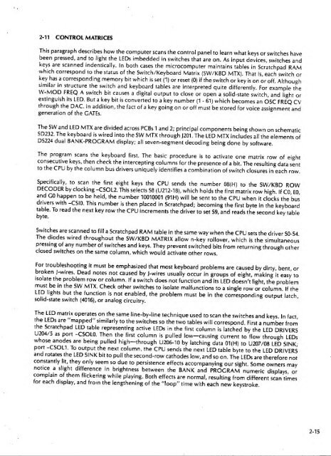
notice a slight difference in brightness between the BANK and PROGRAM numeric displays or^.2-11 CONTROL MATRICESThis paragraph describes how the computer scans the control panel to learn what keys or switches havebeen pressed, and to light the LEDs imbedded in switches that are on. As input devices, switches andkeys are scanned indenticaily. In both cases the microcomputer maintains tables in Scratchpad RAMwhich correspond to the status of the Switch/Keyboard Matrix (SW/KBD MIX). That is, each switch orkey has a corresponding memory bit which is set (1) or reset (0) if the switch or key is on or off. Althoughsimilar instructure the switch and keyboard tables are interpreted quite differently. For example theW-MOD FREQ A switch bit causes a digital output to close or open a solid-state switch, and light orextinguish its LED. But a key bit is converted to a key number (1 - 61) which becomes an OSC FREQ CVthrough the DAG. In addition, the fact of a key going on or off must be stored for voice assignment andgeneration of the CATEs.The SW and LED MTX are divided across PCBs 1 and 2; principal components being shown on schematicSD232. The keyboard is wired into the SW MTX through J201. The LED MTX includes all the elements ofDS224 dual BANK^PROGRAM display; all seven-segment decoding being done by software.The program scans the keyboard first. The basic procedure is to activate one matrix row of eightconsecutive keys, then check the intercepting columns for the presence of a bit. The resulting data sentto the GPU by the column bus drivers uniquely identifies a combination of switch closures in each row.Specifically, to scan the first eight keys the CPU sends the number 08(H) to the SW/KBD ROWDECODER by clocking -CSOL2. This selects 58 (U212-18), which holds the first matrix row high. If CO EOand GO happen to be held, the number 10010001 (91H) will be sent to the CPU when it clocks the bus'drivers with -CSIO. This number is then placed in Scratchpad; becoming the first byte In the keyboardtable. To read the next key row the CPU increments the driver to set S9, and reads the second key tablbyte,'Switches are scanned to fill a Scratchpad RAM table in the same way when the CPU sets the driver S0-S4The diodes wired throughout the SW/KBD MATRIX allow n-key rollover, which is the simultaneouspressing of any number of switches and keys. They prevent switched bits from returning through otherclosed switches on the same column, which would activate other rows.For troubleshooting it must be emphasized that most keyboard problems are caused by dirty bent orbroken J-wires. Dead notes not caused by J-wires usually occur in groups of eight, making it easy toisolate the problem row or column. If a switch does not function and its LED doesn't light, the problemmust be in the SW MTX. Check other switches to isolate malfunctions to a single row or column If theLED lights but the function is not enabled, the problem must be in the corresponding output latchsolid-state switch (4016), or analog circuitry.The LED matrix operates on the same line-by-line technique used to scan the switches and keys. In factthe LEDs are "mapped" similarly to the switches so the two tables will correspond. First a number fromthe Scratchpad LED table representing active LEDs in the first column is latched by the LED DRIVERSU204/5 as port -GSOLO. Then the first column is pulled low-causing current to flow through LEDswhose anodes are being pulled high—through U206-10 by latching data 01(H) to U207/08 LED SINKport -CSOL1. To output the next column, the CPU sends the next LED table byte to the LED DRIVERSand rotates the LED SINK bit to pull the second-row cathodes low, and so on. The LEDs are therefore notconstantly It they only seem so due to persistence effects accompanying our sight. Some owners maycomplain of them flickering while playing. Both effects are normal, resulting from different scan timesfor each display, and from the lengthening of the "loop" time with each new keystroke2-15
2-12 ADC, DAC, AND CV OUTPUTSThe DAC is the essential interface between the control potentiometers and microcomputer andbetween the microcomputer and the synthesizer. It is based on the 16-bit, integrated DAC-71-CSB-I.However, at most, 14 bits are used only for precisely controlling the oscillators while, normally, sevenbits provide adequate resolution for all other computer-processed CVs. The DACs full scale voltage is10.67V, but most CVs are limited to 10V by the software.JFor editing or manual operation, the DAC performs analog-to-digital conversion (ADC).' This isdone byoutputting one of 24 entries from a Scratchpad RAM table of pot settings, at the same time the actualpot isbeing sampled through the ADC "window" comparator (ADC CPR). (Actually, the 10-V DACrange is divided by two for comparison with 5V-range pots.) The comparator signals ADC HI or ADC LOif the pot wiper is actually set below or above the value of the converted table entry. As long as thevoltages don't match, the table value is decremented or incremented until they do match. Once all thepots have been checked, a few adjustments are made (depending on the mode of operation), and theDAC again converts the pot values, this time distributing them and the oscillator and filter CVs to thesynth. Thus, the DAC output, Vdac, steps between 62 values (24 pots + 38 CVs) (during each 6-ms loop.The POT MUX output, Vmux, assumes the value of the settings of ail 24 pots during the first part of eachloop. This is shown in Waveform 2-1a. In Waveform 2-1b, Vdac is shown assuming the 24 comparativepot values and the 38 CVs.A VMUX, U365-9B VDAC, U364-7V:H:2V/div.5 ms/div(approx.)Waveform 2-1VMUX AND VDACThe POT MUX shown is on SD231. Basically, data latched by U211 selects (or, addresses) one of 24 pots ata time, whose wiper voltage becomes the Vmux sent to the ADC comparator. The address latch bits QO,Q1, Q5 have a decimal value 0-7. Waveform 2-2 shows QO toggling when clocked. Applied to the A, B,C, inputs of U201-03, these bits simultaneously select one of eight inputs on each 4051. When high the Iinputs inhibit the 4051; so to select just one pot, Q2, Q3, or Q4 must be low.2-16
- Page 1 and 2: ^^. ^ ^s .y ^,-j?^ ^^w^-^>&i^^^V^?v
- Page 3 and 4: PROPHET-5 SYNTHESIZERTECHNICAL MANU
- Page 5 and 6: iJTable of ContentsISECTION 1MECHAN
- Page 7 and 8: '1SECTION 1MECHANICAL1-0 GENERALThi
- Page 9 and 10: Raise the top panel assembly to ser
- Page 11 and 12: 1-5 PCB 1/2 CONTROL PANELSOnce PCB
- Page 13 and 14: Figure 1-5KEYBOARD REMOVAL1 -7/1 -8
- Page 15 and 16: TOADDITIONALVCOsTOADDITIONALENV GEN
- Page 17 and 18: 2-2 THE PROPHETThe Prophet is a sub
- Page 19 and 20: COMMON ANALOGVOICE(VOiCES e-5 ARE S
- Page 21 and 22: 'IAll processed CVs originate from
- Page 23 and 24: ajMim—2-8 AUDIO OUTPUTAs shown in
- Page 25 and 26: .'2-10 MICROPROCESSOR, MEMORY, AND
- Page 27: For troubleshooting, it should be e
- Page 31 and 32: iirH- - jMg 1— -^ 'iVMUX, U201-3^
- Page 33 and 34: the same CV and trigger pattern to
- Page 35 and 36: SECTION 3DOCUMENTS3-0 DOCUMENT LIST
- Page 37 and 38: TOP PANEL ASSEMBLY1CHASSiSLAST \NOT
- Page 39 and 40: TB/0i/20f 32 22 30 20 19 25 233 2 I
- Page 41 and 42: TBZOf/^fOtP^2C20ZTBZOI/IOl17FUT ATK
- Page 43 and 44: OA* Y*tMOlooMtt'O o)i:i'^.^^.1 I5-
- Page 45 and 46: —' i+6V+5d^1—+I5V+ SV+ V ff^ U3
- Page 47 and 48: 1+ I5V£/JJiJ-5|T> -TUNEWBOtWfOiAMP
- Page 50 and 51: P40I+I6V(TUNE MUX)P40iP40f3ft wMIK
- Page 52 and 53: + I5VOSCP40i^Q ^ |PMOPFR£QASFINAL
- Page 54 and 55: M+I5VP40/ x|5v301 K|%34^fM0O£WASR4
- Page 56 and 57: IU504ft50647C5042Z00|iFMCTBMtZCT2 1
- Page 58 and 59: Inpreparation for service, set up t
- Page 60 and 61: 4-2 OSCILLATOR B TESTSTEP MODULE CO
- Page 62 and 63: 4-S FILTER TEST.STEP'MODULE CONTROL
- Page 64 and 65: 4-8 POLY-MOD TEST—A.STEP MODULE C
- Page 66 and 67: i4-11 PITCH WHEEL TRIMThis trim rem
- Page 68 and 69: A)I4-16 VCO SCALE TRIMBE SURE RECOR
- Page 70 and 71: 4-19 FILTER ENVELOPE AMOUNT VCA BAL
- Page 72 and 73: 4-21 FINAL VGA BAL1. Switch PRESET
- Page 74 and 75: 115-3 PCB 3BT301 E-040L-\:!Oi 0-U45
- Page 76 and 77: I ]U374U375U376U377U37SU379U380U381
- Page 78 and 79:
1R419SR4199R4200R4201R4202R4203R420
- Page 80 and 81:
51» IR44S7/488 R-025R44S9 R-009R44
- Page 82 and 83:
kL096 E-066098 E-071100 E-078102 E-
- Page 84 and 85:
IJ310 M-156312 M-157314 M-158316 M-
- Page 86 and 87:
JJ51S R-161520 R--162522 R-163524 R
- Page 88 and 89:
FFFFDBKFETFFFILTFINFINEFOAFREQFSKFT
- Page 90 and 91:
11 IJSECTION 8THEORY8-0 INTRODUCTIO
- Page 92 and 93:
1 1for the 2 to 5-foot range. The c
- Page 94 and 95:
IiSECTION 9PRCX^RAMMING9-0 INTRODUC
- Page 96 and 97:
I3JIJThe Prophet will not accept st
- Page 98 and 99:
ByteByte 23Switch Bit (7)OSC A PULS
- Page 100 and 101:
t J IISECTION 10REVISION 3.1 and 3.
- Page 102 and 103:
I+ I5V+5dI^1-+5V 2'2pF+I6V+5V^^' U3
- Page 104 and 105:
T&=* PANEL ASSE^^mtYSAfKEYBOARD,'r-
- Page 106 and 107:
.^^'»_ u jj'/X H"r,P-*tQ( p5^f -^"
- Page 108 and 109:
4/J«-5[E> -TUNER57a12wzofwiOi^^^^^
- Page 110 and 111:
—T8502J/fRSOBWMfrS/IC5045.iiU502i
- Page 112 and 113:
^ 1 1 ;4 PINFigure II-OFigure11-TM1
- Page 114 and 115:
I 111-2 REVISION 3.0 MEMORY TESTRev
- Page 116 and 117:
Tr1 1-5 WHEEL BALANCE TRIM1. See pa
- Page 118 and 119:
SECTION 13PROPHET-5 REV 3.3 UPDATET
- Page 120 and 121:
iFigure 13-1PCB 3 TOP MODIFICATIONT
- Page 122 and 123:
T 1ttSillniiinMIttltltlltlillll^- ^
- Page 124 and 125:
i/*5-tft/jj4-y,6-C90H202 >7-CS0H5Q3
- Page 126 and 127:
'^'K'..v''
- Page 128 and 129:
tV t IEPROM1000.3.0V.8.0V.8.1V.8.21
- Page 130 and 131:
IJmemory interface1000.3.01000.3.11
- Page 132 and 133:
ittKRAM, non-volatile (NV)1000.3.01
- Page 134:
1voltage-current convertervoice ass