DM74LS244 Octal 3-STATE Buffer/Line Driver/Line Receiver
DM74LS244 Octal 3-STATE Buffer/Line Driver/Line Receiver
DM74LS244 Octal 3-STATE Buffer/Line Driver/Line Receiver
- No tags were found...

Create successful ePaper yourself
Turn your PDF publications into a flip-book with our unique Google optimized e-Paper software.
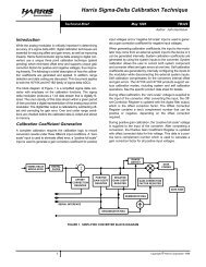
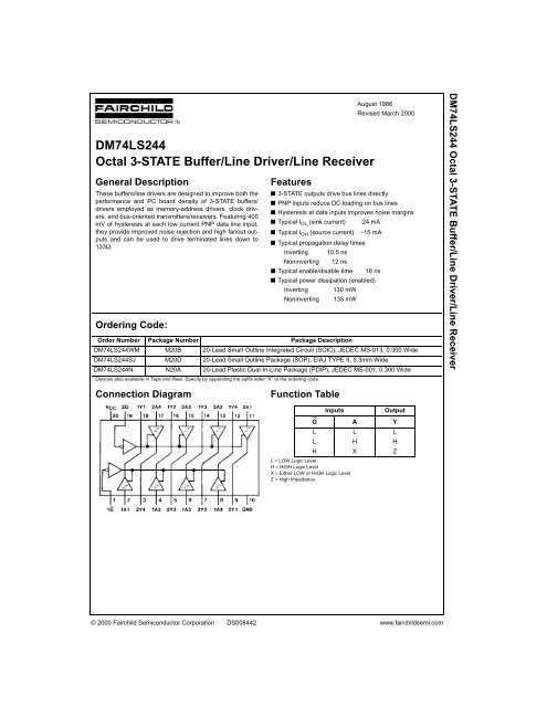
<strong>DM74LS244</strong><strong>Octal</strong> 3-<strong>STATE</strong> <strong>Buffer</strong>/<strong>Line</strong> <strong>Driver</strong>/<strong>Line</strong> <strong>Receiver</strong>General DescriptionThese buffers/line drivers are designed to improve both theperformance and PC board density of 3-<strong>STATE</strong> buffers/drivers employed as memory-address drivers, clock drivers,and bus-oriented transmitters/receivers. Featuring 400mV of hysteresis at each low current PNP data line input,they provide improved noise rejection and high fanout outputsand can be used to drive terminated lines down to133Ω.Ordering Code:FeaturesAugust 1986Revised March 2000■ 3-<strong>STATE</strong> outputs drive bus lines directly■ PNP inputs reduce DC loading on bus lines■ Hysteresis at data inputs improves noise margins■ Typical I OL (sink current) 24 mA■ Typical I OH (source current) −15 mA■ Typical propagation delay timesInverting 10.5 nsNoninverting 12 ns■ Typical enable/disable time 18 ns■ Typical power dissipation (enabled)Inverting 130 mWNoninverting 135 mWOrder Number Package Number Package Description<strong>DM74LS244</strong>WM M20B 20-Lead Small Outline Integrated Circuit (SOIC), JEDEC MS-013, 0.300 Wide<strong>DM74LS244</strong>SJ M20D 20-Lead Small Outline Package (SOP), EIAJ TYPE II, 5.3mm Wide<strong>DM74LS244</strong>N N20A 20-Lead Plastic Dual-In-<strong>Line</strong> Package (PDIP), JEDEC MS-001, 0.300 WideDevices also available in Tape and Reel. Specify by appending the suffix letter “X” to the ordering code.<strong>DM74LS244</strong> <strong>Octal</strong> 3-<strong>STATE</strong> <strong>Buffer</strong>/<strong>Line</strong> <strong>Driver</strong>/<strong>Line</strong> <strong>Receiver</strong>Connection DiagramFunction TableInputsOutputG A YL L LL H HH X ZL = LOW Logic LevelH = HIGH Logic LevelX = Either LOW or HIGH Logic LevelZ = High Impedance© 2000 Fairchild Semiconductor Corporation DS008442 www.fairchildsemi.com
<strong>DM74LS244</strong>Absolute Maximum Ratings(Note 1)Supply Voltage7VInput Voltage7VOperating Free Air Temperature Range 0°C to +70°CStorage Temperature Range−65°C to +150°CNote 1: The “Absolute Maximum Ratings” are those values beyond whichthe safety of the device cannot be guaranteed. The device should not beoperated at these limits. The parametric values defined in the ElectricalCharacteristics tables are not guaranteed at the absolute maximum ratings.The “Recommended Operating Conditions” table will define the conditionsfor actual device operation.Recommended Operating ConditionsSymbol Parameter Min Nom Max UnitsV CC Supply Voltage 4.75 5 5.25 VV IH HIGH Level Input Voltage 2 VV IL LOW Level Input Voltage 0.8 VI OH HIGH Level Output Current −15 mAI OL LOW Level Output Current 24 mAT A Free Air Operating Temperature 0 70 °CElectrical Characteristicsover recommended operating free air temperature range (unless otherwise noted)Symbol Parameter ConditionsMin Typ Max(Note 2)UnitsV I Input Clamp Voltage V CC = Min, I I = −18 mA −1.5 VHYS Hysteresis (V T+ − V T− ) V CC = Min 0.2 0.4 VData Inputs OnlyV OH HIGH Level Output Voltage V CC = Min, V IH = MinV IL = Max, I OH = −1 mA2.7V CC = Min, V IH = MinV IL = Max, I OH = −3 mA2.4 3.4 VV CC = Min, V IH = MinV IL = 0.5V, I OH = Max2V OL LOW Level Output Voltage V CC = Min I OL = 12 mA 0.4V IL = Max I OL = Max 0.5 VV IH = MinI OZH Off-State Output Current, V CC = Max V O = 2.7V 20 µAHIGH Level Voltage AppliedV IL = MaxI OZL Off-State Output Current, V IH = Min V O = 0.4V −20 µALOW Level Voltage AppliedI I Input Current at Maximum V CC = Max V I = 7V 0.1 mAInput VoltageI IH HIGH Level Input Current V CC = Max V I = 2.7V 20 µAI IL LOW Level Input Current V CC = Max V I = 0.4V −0.5 −200 µAI OS Short Circuit Output Current V CC = Max (Note 3) −40 −225 mAI CC Supply Current V CC = Max, Outputs HIGH 13 23Outputs Open Outputs LOW 27 46 mAOutputs Disabled 32 54Note 2: All typicals are at V CC = 5V, T A = 25°C.Note 3: Not more than one output should be shorted at a time, and the duration should not exceed one second.www.fairchildsemi.com 2
Switching Characteristicsat V CC = 5V, T A = 25°CSymbol Parameter Conditions Max Unitst PLH Propagation Delay Time C L = 45 pFLOW-to-HIGH Level OutputR L = 667Ω18 nst PHL Propagation Delay Time C L = 45 pFHIGH-to-LOW Level OutputR L = 667Ω18 nst PZL Output Enable Time to C L = 45 pFLOW LevelR L = 667Ω30 nst PZH Output Enable Time to C L = 45 pFHIGH LevelR L = 667Ω23 nst PLZ Output Disable Time C L = 5 pFfrom LOW LevelR L = 667Ω25 nst PHZ Output Disable Time C L = 5 pFfrom HIGH LevelR L = 667Ω18 nst PLH Propagation Delay Time C L = 150 pFLOW-to-HIGH Level OutputR L = 667Ω21 nst PHL Propagation Delay Time C L = 150 pFHIGH-to-LOW Level OutputR L = 667Ω22 nst PZL Output Enable Time to C L = 150 pFLOW LevelR L = 667Ω33 nst PZH Output Enable Time to C L = 150 pFHIGH LevelR L = 667Ω26 ns<strong>DM74LS244</strong>3 www.fairchildsemi.com
<strong>DM74LS244</strong>Physical Dimensions inches (millimeters) unless otherwise noted20-Lead Small Outline Integrated Circuit (SOIC), JEDEC MS-013, 0.300 WidePackage Number M20Bwww.fairchildsemi.com 4
Physical Dimensions inches (millimeters) unless otherwise noted (Continued)<strong>DM74LS244</strong>20-Lead Small Outline Package (SOP), EIAJ TYPE II, 5.3mm WidePackage Number M20D5 www.fairchildsemi.com
<strong>DM74LS244</strong> <strong>Octal</strong> 3-<strong>STATE</strong> <strong>Buffer</strong>/<strong>Line</strong> <strong>Driver</strong>/<strong>Line</strong> <strong>Receiver</strong>Physical Dimensions inches (millimeters) unless otherwise noted (Continued)20-Lead Plastic Dual-In-<strong>Line</strong> Package (PDIP), JEDEC MS-001, 0.300 WidePackage Number N20AFairchild does not assume any responsibility for use of any circuitry described, no circuit patent licenses are implied andFairchild reserves the right at any time without notice to change said circuitry and specifications.LIFE SUPPORT POLICYFAIRCHILD’S PRODUCTS ARE NOT AUTHORIZED FOR USE AS CRITICAL COMPONENTS IN LIFE SUPPORTDEVICES OR SYSTEMS WITHOUT THE EXPRESS WRITTEN APPROVAL OF THE PRESIDENT OF FAIRCHILDSEMICONDUCTOR CORPORATION. As used herein:1. Life support devices or systems are devices or systemswhich, (a) are intended for surgical implant into thebody, or (b) support or sustain life, and (c) whose failureto perform when properly used in accordance withinstructions for use provided in the labeling, can be reasonablyexpected to result in a significant injury to theuser.www.fairchildsemi.com 62. A critical component in any component of a life supportdevice or system whose failure to perform can be reasonablyexpected to cause the failure of the life supportdevice or system, or to affect its safety or effectiveness.www.fairchildsemi.com
This datasheet has been downloaded from:www.DatasheetCatalog.comDatasheets for electronic components.