Harris Sigma-Delta Calibration Technique
Harris Sigma-Delta Calibration Technique
Harris Sigma-Delta Calibration Technique

You also want an ePaper? Increase the reach of your titles
YUMPU automatically turns print PDFs into web optimized ePapers that Google loves.
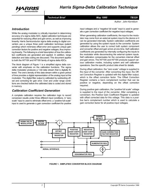
Semiconductor<strong>Harris</strong> <strong>Sigma</strong>-<strong>Delta</strong> <strong>Calibration</strong> <strong>Technique</strong>Technical Brief May 1995 TB329Author: John KornblumIntroductionWhile the analog modulator is critically important in determiningaccuracy of a sigma delta ADC, digital calibration techniques areessential for reducing offset and gain errors, as well as improvinglinearity. <strong>Harris</strong> Semiconductor sigma delta analog to digital convertersuse a unique three point calibration technique (patentpending) which minimizes offset error and supports unique gaincorrection factors for positive and negative voltages, thus improvinglinearity. The following is a brief description of how the calibrationcoefficients are generated and applied. In addition, rangedetection and data coding are discussed. This document appliesto both the HI719X and HI718X family of sigma delta ADCs.The block diagram of Figure 1 is a simplified sigma delta converterwith emphasis on the calibration functions. The sigmadelta modulator produces a 1-bit data stream that is digitally filtered.The one’s density of this data stream within a given periodof time provides a digital representation of the analog input at themodulator. The digital filter output is calibrated by subtracting offsetand correcting for gain error. Over and under range conditionsare checked before the calibrated data is coded and storedin memory.<strong>Calibration</strong> Coefficient GenerationA complete calibration requires the calibration logic to recordconversion results under three different input conditions. A “zeroscale” input is used to eliminate offset error, a “positive full scale”input is used to generate a gain correction coefficient for positiveinput voltages and a “negative full scale” input is used to generatea gain correction coefficient for negative input voltages.When generating calibration coefficients, the input to the modulatormay come from an external system input to the device or itcan be generated internally. System calibration coefficients aregenerated by using the system inputs to the converter. Systemcalibration allows the user to correct both system componentand converter offset and gain errors at one time. Self calibrationcoefficients are generated by internally configuring the inputs tothe modulator while disconnecting the external system inputs.Self calibration compensates for the converters internal offsetand gain errors. The HI719X and HI718X products support variouscalibration modes, including system and self calibrationoperations. See the specific product data sheet for details.During offset calibration, the “zero scale” voltage is supplied tothe input of the converter. After converting this input, the OffsetCorrection Register is updated with the digital filter output,which is the offset correction factor. The Offset CorrectionRegister contains a two’s complement number that can bepositive or negative, depending on the offset correctionrequired.During positive gain calibration, the “positive full scale” voltageis supplied to the input of the converter. After completing aconversion, the Positive Gain Coefficient Register is updatedwith offset corrected data for this voltage. This data is a positivetwo’s complement number which is used to calculate again correction factor for all positive input voltages.SIGMA DELTAMODULATORDIGITALFILTER+∑-RANGEDETECTDATACODINGOFFSETCORRECTIONREGISTERPOSITIVEGAIN COEFFREGISTERNEGATIVEGAIN COEFFREGISTERGAIN CORRECTIONFACTOR REGISTERDATA RAMNUMERATOR REGSERIAL INTERFACENDDENOMINATOR REGFIGURE 1. SIMPLIFIED CONVERTER BLOCK DIAGRAM1Copyright © <strong>Harris</strong> Corporation 1998
Technical Brief 329During negative gain calibration, the “negative full scale” voltageis supplied to the input of the converter. After completinga conversion, the Negative Gain Coefficient Register isupdated with offset corrected data for this voltage. This data isa negative two’s complement number which is used to calculatea gain correction factor for all negative input voltages.The order of the gain coefficient generation is not important butthe offset coefficient must be generated before either of the gaincoefficients. For proper calibration, the gain coefficients musthave offset error removed before storage in memory. The flowchart below describes a proper method for generating the convertercalibration coefficients using the system inputs.CALIBRATIONROUTINEAPPLY ZERO SCALE INPUTPROGRAM DEVICE FOROFFSET CALIBRATIONOUTPUTINTERRUPTACTIVE?YESAPPLY POSITIVEFULL SCALE INPUTPROGRAM DEVICE FORPOSITIVE GAIN CALIBRATIONOUTPUTINTERRUPTACTIVE?YESAPPLY NEGATIVEFULL SCALE INPUTPROGRAM DEVICE FORNEGATIVE GAIN CALIBRATIONOUTPUTINTERRUPTACTIVE?YESCALIBRATIONROUTINECOMPLETEFIGURE 2.NONONOCalibrating Conversion ResultsIn normal operating mode, every conversion is followed by adata calibration phase. Data calibration is as follows:1. Offset is subtracted.2. The polarity of the offset corrected data is determined andthe proper gain correction factor is generated.3. The offset calibrated data is multiplied by the gain correctionfactor generated in step two. This completes gaincalibration.4. The offset corrected data is checked for over or underrange error before final coding (two’s complement, offsetbinary or, in unipolar mode, binary).The calibrated, coded data is stored in memory and the useris notified of a completed conversion via an output interruptsignal.Offset <strong>Calibration</strong>Offset <strong>Calibration</strong> is a simple two’s complement subtraction.Each conversion has offset error removed by subtracting thecontents of the Offset Correction Register from the digital filteroutput.Gain <strong>Calibration</strong>Gain calibration is a two step process. First, the proper gaincorrection factor is generated. Then this factor is multipliedby the offset corrected data, completing gain calibration.The gain correction factor is generated via the divider (N/D)shown in Figure 1. After offset calibration has been completed,the converter determines which gain coefficient touse for generation of the gain correction factor. If the offsetcorrected data is positive, the positive gain coefficient is thedenominator when determining the gain correction factor. Ifthe offset corrected data is negative, the two’s complementof the negative gain coefficient is the denominator whendetermining the gain correction factor.The input span (numerator), used to generate the gain correctionfactor is different for bipolar versus unipolar mode. Inunipolar mode the calibration logic determines the gain correctionfactor by dividing the total internal resolution of theconverter (2 N ) by the span between the zero scale and positivefull scale points. In bipolar mode the gain factor is determinedby dividing one half the total internal resolution (2 N-1 )of the converter by the span between the zero scale (bipolarmidscale) and ± full scale points.In either unipolar or bipolar mode, the division result is thegain correction factor and is multiplied by the offset correctedfilter output to calculate the proper digital output of the converter.The gain correction factor is not permanently storedbut is generated for each conversion. The Gain CorrectionFactor Register is not accessible via the serial interface.Range DetectionIn addition to the calibration process, the converter detects overrange above positive full scale and under range below minusfull scale conditions. Over or under range detection affects theoutput data coding as described in the Data Coding section.2
Technical Brief 329Over range detection is identical for both bipolar and unipolaroperation. Over range is detected by comparing the offsetcorrected filter output to the positive gain coefficient. If thecurrent offset corrected filter value is greater than the positivegain coefficient, an over range condition is detected.In unipolar mode, under range is detected by sampling thesign bit of the offset calibrated data. If the sign bit is logic 1,signifying a negative voltage, an under range condition exists.In bipolar mode, under range is detected by comparing theoffset corrected filter output to the negative gain coefficient.If the current offset corrected filter value is less than the negativegain coefficient, an under range condition is detected.Data CodingThe calibrated data can be obtained in one of variousnumerical codes depending on the bipolar/unipolar mode bitand the two’s complement coding bit. In bipolar mode, if thetwo’s complement bit is true, the output is two’s complement.In bipolar mode, offset binary coding is used when the two’scomplement coding bit is not true. In unipolar mode, onlybinary coding is available and the two’s complement codingbit is a don’t care.The output coding tables for the HI719X 24-bit family ofproducts is shown below. V ZS represents the applied zeroscale input during system calibration or is AGND if internalcalibration was performed. V PFS represents the applied positivefull scale input during system calibration or is V REF ifinternal calibration was performed. V NFS represents theapplied negative full scale input during system calibration oris -V REF if internal calibration was performed.TABLE 1. BIPOLAR MODE OUTPUT CODES 24-BITINPUT VOLTAGETWO’SCOMPLEMENTCODEOFFSETBINARY CODETABLE 2. UNIPOLAR MODE DATA OUTPUT CODES 24-BITINPUT VOLTAGE BINARY CODE>(V PFS - 1.5 LSB)V PFS - 1.5 LSBV PFS /2 - 0.5 LSBWhen the range detection logic determines an over range,the converter output will clamp at the >(V PFS - 1.5 LSB) outputas described in Table 1 or 2. When the range detectionlogic determines an under range, the converter output willclamp at the