2000 - Draper Laboratory
2000 - Draper Laboratory
2000 - Draper Laboratory
- No tags were found...

You also want an ePaper? Increase the reach of your titles
YUMPU automatically turns print PDFs into web optimized ePapers that Google loves.
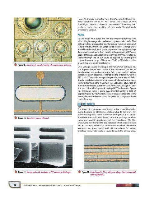
Figure 16 shows a fabricated "race-track" design that has a linearlypolarized stripe of PZT down the center of thediaphragm. Figure 17 shows a cross section of an array thathas been cracked to reveal the hole side-walls. The etch wallsare close to vertical.Figure 15. Circular pixels are poled radially with concentric ring electrodes.POLING16 x 16 arrays were poled one row at a time using a probe cardwith 16 high-voltage electrodes and 1 ground electrode. Thepoling voltage was applied slowly using a ramp up, soak, andramp down of 2 min each. Large series resistors (40 MΩ) wereadded in series with each probe to prevent damaging the chipif any pixel contained a short circuit. Voltages up to 800 V wereapplied this way. Voltages between 800 and 1000 V resulted insparks through the air, but could be applied by covering thechip with several drops of Fluorinert FC-77 (a 3M dielectric fluid),which prevents air breakdown.Over-voltage caused cracking of the PZT, shown in Figure 18.The applied electric field causes a tensile strain of the PZT inthe direction perpendicular to the field equal to d 31 E. Whenthe tensile strain becomes too large (on the order of 0.3%), thePZT cracks. The cracks always form parallel to the electric field.Special breakdown test structures were included on the maskset for determining the maximum safe voltage as a function ofinter-electrode gap. Data on crack formation voltage for severaltest chips with 3-µm-thick sol-gel PZT is shown in Figure19. Although there is some experimental scatter, a field ofapproximately 20 V/µm was necessary to cause cracks to form;hence, the active devices could be poled at 10 V/µm with nocracks forming.TEST RESULTS RESULTSFigure 16. "Race-track" pixel as fabricated.The large 16 x 16 arrays were tested at Lockheed Martin bybump-bonding an electronics readout chip to the array. Inhousetesting was carried out by mounting small 3 x 3 arraysinto Kovar flat-packs with holes cut in the package to allowwater and acoustic signals to reach the chip (Figure 20). Thechips were wire-bonded to the flat-pack, which was solderedto a PC board, to which coax cables were attached. The entireassembly was then coated with silicone rubber for waterproofing,with a hole to allow sound to reach the sensor array.Figure 17. Through-wafer hole terminates on PZT monomorph diaphragm.Figure 18. Cracks formed in PZT by poling overvoltage. Cracks form parallelto the electric field.10Advanced MEMS Ferroelectric Ultrasound 2-Dimensional Arrays