CS5531/32/33/34 - Eshop-Rychle.cz
CS5531/32/33/34 - Eshop-Rychle.cz
CS5531/32/33/34 - Eshop-Rychle.cz

You also want an ePaper? Increase the reach of your titles
YUMPU automatically turns print PDFs into web optimized ePapers that Google loves.
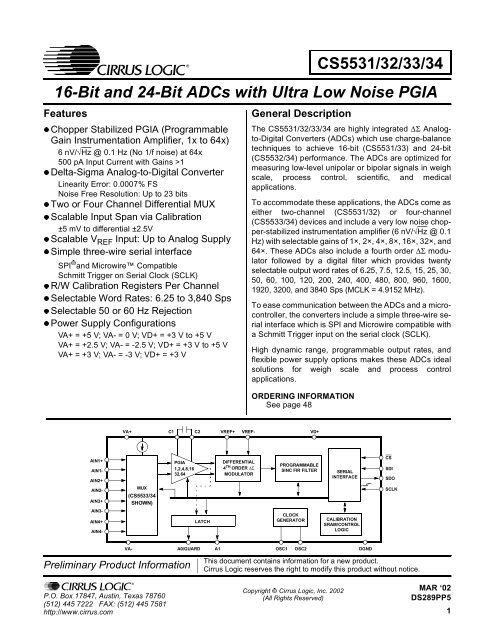
<strong>CS5531</strong>/<strong>32</strong>/<strong>33</strong>/<strong>34</strong>16-Bit and 24-Bit ADCs with Ultra Low Noise PGIAFeaturesChopper Stabilized PGIA (ProgrammableGain Instrumentation Amplifier, 1x to 64x)6nV/√Hz @ 0.1 Hz (No 1/f noise) at 64x500 pA Input Current with Gains >1Delta-Sigma Analog-to-Digital ConverterLinearity Error: 0.0007% FSNoise Free Resolution: Up to 23 bitsTwo or Four Channel Differential MUXScalable Input Span via Calibration±5 mV to differential ±2.5VScalable V REF Input: Up to Analog SupplySimple three-wire serial interfaceSPI and Microwire CompatibleSchmitt Trigger on Serial Clock (SCLK)R/W Calibration Registers Per Channel®Selectable Word Rates: 6.25 to 3,840 SpsSelectable 50 or 60 Hz RejectionPower Supply ConfigurationsVA+=+5V;VA-=0V;VD+=+3Vto+5VVA+=+2.5V;VA-=-2.5V;VD+=+3Vto+5VVA+ = +3 V; VA- = -3 V; VD+ = +3 VGeneral DescriptionThe <strong>CS5531</strong>/<strong>32</strong>/<strong>33</strong>/<strong>34</strong> are highly integrated ∆Σ Analogto-DigitalConverters (ADCs) which use charge-balancetechniques to achieve 16-bit (<strong>CS5531</strong>/<strong>33</strong>) and 24-bit(CS55<strong>32</strong>/<strong>34</strong>) performance. The ADCs are optimized formeasuring low-level unipolar or bipolar signals in weighscale, process control, scientific, and medicalapplications.To accommodate these applications, the ADCs come aseither two-channel (<strong>CS5531</strong>/<strong>32</strong>) or four-channel(CS55<strong>33</strong>/<strong>34</strong>) devices and include a very low noise chopper-stabilizedinstrumentation amplifier (6 nV/√Hz @0.1Hz) with selectable gains of 1×, 2×, 4×, 8×, 16×, <strong>32</strong>×, and64×. These ADCs also include a fourth order ∆Σ modulatorfollowed by a digital filter which provides twentyselectable output word rates of 6.25, 7.5, 12.5, 15, 25, 30,50, 60, 100, 120, 200, 240, 400, 480, 800, 960, 1600,1920, <strong>32</strong>00, and 3840 Sps (MCLK = 4.9152 MHz).To ease communication between the ADCs and a microcontroller,the converters include a simple three-wire serialinterface which is SPI and Microwire compatible witha Schmitt Trigger input on the serial clock (SCLK).High dynamic range, programmable output rates, andflexible power supply options makes these ADCs idealsolutions for weigh scale and process controlapplications.ORDERING INFORMATIONSee page 48VA+ C1 C2 VREF+ VREF- VD+AIN1+AIN1-AIN2+AIN2-AIN3+AIN3-AIN4+AIN4-MUX(CS55<strong>33</strong>/<strong>34</strong>SHOWN)PGIA1,2,4,8,16<strong>32</strong>,64LATCHDIFFERENTIAL4 TH ORDER ∆ΣMODULATORPROGRAMMABLESINC FIR FILTERCLOCKGENERATORSERIALINTERFACECALIBRATIONSRAM/CONTROLLOGICCSSDISDOSCLKVA-A0/GUARDPreliminary Product InformationA1OSC1OSC2DGNDThis document contains information for a new product.Cirrus Logic reserves the right to modify this product without notice.P.O. Box 17847, Austin, Texas 78760(512) 445 7222 FAX: (512) 445 7581http://www.cirrus.comCopyright © Cirrus Logic, Inc. 2002(All Rights Reserved)MAR ‘02DS289PP51
<strong>CS5531</strong>/<strong>32</strong>/<strong>33</strong>/<strong>34</strong>TABLE OF CONTENTS1. CHARACTERISTICS AND SPECIFICATIONS ..........................................................5ANALOG CHARACTERISTICS..........................................................................5TYPICAL RMS NOISE (NV), <strong>CS5531</strong>/<strong>32</strong>/<strong>33</strong>/<strong>34</strong>-AS ...........................................8TYPICAL NOISE FREE RESOLUTION(BITS), CS55<strong>32</strong>/<strong>34</strong>-AS .........................8TYPICAL RMS NOISE (NV), CS55<strong>32</strong>/<strong>34</strong>-BS .....................................................9TYPICAL NOISE FREE RESOLUTION(BITS), CS55<strong>32</strong>/<strong>34</strong>-BS .........................95 V DIGITAL CHARACTERISTICS ..................................................................103 V DIGITAL CHARACTERISTICS ..................................................................10DYNAMIC CHARACTERISTICS ......................................................................11ABSOLUTE MAXIMUM RATINGS ...................................................................11SWITCHING CHARACTERISTICS ..................................................................122. GENERAL DESCRIPTION .......................................................................................142.1. Analog Input ....................................................................................................142.1.1. Analog Input Span .................................................................................... 152.1.2. Multiplexed Settling Limitations ............................................................152.1.3. Voltage Noise Density Performance .....................................................152.1.4. No Offset DAC ......................................................................................152.2. Overview of ADC Register Structure and Operating Modes ............................162.2.1. System Initialization ..............................................................................172.2.2. Command Register Quick Reference ..................................................192.2.3. Command Register Descriptions ..........................................................202.2.4. Serial Port Interface ..............................................................................242.2.5. Reading/Writing On-Chip Registers ......................................................252.3. Configuration Register .....................................................................................252.3.1. Power Consumption .............................................................................252.3.2. System Reset Sequence ......................................................................252.3.3. Input Short ............................................................................................262.3.4. Guard Signal .........................................................................................262.3.5. Voltage Reference Select .....................................................................262.3.6. Output Latch Pins .................................................................................262.3.7. Offset and Gain Select ..........................................................................27Contacting Cirrus Logic SupportFor a complete listing of Direct Sales, Distributor, and Sales Representative contacts, visit the Cirrus Logic web site at:http://www.cirrus.com/corporate/contacts/sales.cfmSPI is a registered trademark of International Business Machines Corporation.Microwire is a trademark of National Semiconductor Corporation.IMPORTANT NOTICE"Preliminary" product information describes products that are in production, but for which full characterization data is not yet available. "Advance" product informationdescribes products that are in development and subject to development changes. Cirrus Logic, Inc. and its subsidiaries ("Cirrus") believe that the informationcontained in this document is accurate and reliable. However, the information is subject to change without notice and is provided "AS IS" without warrantyof any kind (express or implied). Customers are advised to obtain the latest version of relevant information to verify, before placing orders, that information beingrelied on is current and complete. All products are sold subject to the terms and conditions of sale supplied at the time of order acknowledgment, including thosepertaining to warranty, patent infringement, and limitation of liability. No responsibility is assumed by Cirrus for the use of this information, including use of thisinformation as the basis for manufacture or sale of any items, or for infringement of patents or other rights of third parties. This document is the property of Cirrusand by furnishing this information, Cirrus grants no license, express or implied under any patents, mask work rights, copyrights, trademarks, trade secrets orother intellectual property rights. Cirrus owns the copyrights of the information contained herein and gives consent for copies to be made of the information onlyfor use within your organization with respect to Cirrus integrated circuits or other parts of Cirrus. This consent does not extend to other copying such as copyingfor general distribution, advertising or promotional purposes, or for creating any work for resale.An export permit needs to be obtained from the competent authorities of the Japanese Government if any of the products or technologies described in thismaterialand controlled under the "Foreign Exchange and Foreign Trade Law" is to be exported or taken out of Japan. An export license and/or quota needs to beobtained from the competent authorities of the Chinese Government if any of the products or technologies described in this material is subject to the PRC ForeignTrade Law and is to be exported or taken out of the PRC.CERTAIN APPLICATIONS USING SEMICONDUCTOR PRODUCTS MAY INVOLVE POTENTIAL RISKS OF DEATH, PERSONAL INJURY, OR SEVEREPROPERTY OR ENVIRONMENTAL DAMAGE ("CRITICAL APPLICATIONS"). CIRRUS PRODUCTS ARE NOT DESIGNED, AUTHORIZED, OR WARRANT-ED TO BE SUITABLE FOR USE IN LIFE-SUPPORT DEVICES OR SYSTEMS OR OTHER CRITICAL APPLICATIONS. INCLUSION OF CIRRUS PRODUCTSIN SUCH APPLICATIONS IS UNDERSTOOD TO BE FULLY AT THE CUSTOMER'S RISK.Cirrus Logic, Cirrus, and the Cirrus Logic logo designs are trademarks of Cirrus Logic, Inc. All other brand and product names in this document may be trademarksor service marks of their respective owners.2 DS289PP5
<strong>CS5531</strong>/<strong>32</strong>/<strong>33</strong>/<strong>34</strong>2.3.8. Filter Rate Select ..................................................................................272.3.9. Configuration Register Descriptions .....................................................282.4. Setting up the CSRs for a Measurement .........................................................292.4.1. Channel-Setup Register Descriptions ................................................. 302.5. Calibration .......................................................................................................<strong>32</strong>2.5.1. Calibration Registers ............................................................................<strong>32</strong>2.5.2. Gain Register ......................................................................................<strong>32</strong>2.5.3. Offset Register ....................................................................................<strong>32</strong>2.5.4. Performing Calibrations ........................................................................3<strong>32</strong>.5.5. Self Calibration .....................................................................................3<strong>32</strong>.5.6. System Calibration ...............................................................................<strong>34</strong>2.5.7. Calibration Tips ....................................................................................<strong>34</strong>2.5.8. Limitations in Calibration Range ........................................................... 352.6. Performing Conversions ..................................................................................352.6.1. Single Conversion Mode ......................................................................352.6.2. Continuous Conversion Mode .............................................................. 362.6.3. Examples of Using CSRs to Perform Conversions and Calibrations ... 372.7. Using Multiple ADCs Synchronously ...............................................................382.8. Conversion Output Coding ..............................................................................382.8.1. Conversion Data Output Descriptions ..................................................392.9. Digital Filter .....................................................................................................402.10. Clock Generator ..............................................................................................412.11. Power Supply Arrangements ........................................................................... 412.12. Getting Started ................................................................................................452.13. PCB Layout .....................................................................................................453. PIN DESCRIPTIONS ...............................................................................................46Clock Generator .............................................................................................. 46Control Pins and Serial Data I/O ..................................................................... 46Measurement and Reference Inputs ............................................................... 47Power Supply Connections ............................................................................. 474. SPECIFICATION DEFINITIONS ...............................................................................485. ORDERING GUIDE ..................................................................................................486. PACKAGE DRAWINGS ...........................................................................................49DS289PP5 3
LIST OF FIGURES<strong>CS5531</strong>/<strong>32</strong>/<strong>33</strong>/<strong>34</strong>Figure 1. SDI Write Timing (Not to Scale) ...............................................................................13Figure 2. SDO Read Timing (Not to Scale) .............................................................................13Figure 3. Multiplexer Configuration .........................................................................................14Figure 4. Input models for AIN+ and AIN- pins .......................................................................15Figure 5. Measured Voltage Noise Density.............................................................................15Figure 6. <strong>CS5531</strong>/<strong>32</strong>/<strong>33</strong>/<strong>34</strong> Register Diagram ........................................................................16Figure 7. Command and Data Word Timing............................................................................24Figure 8. Guard Signal Shielding Scheme ..............................................................................26Figure 9. Input Reference Model when VRS = 1.....................................................................27Figure 10. Input Reference Model when VRS = 0...................................................................27Figure 11. Self Calibration of Offset ........................................................................................<strong>34</strong>Figure 12. Self Calibration of Gain ..........................................................................................<strong>34</strong>Figure 13. System Calibration of Offset ..................................................................................<strong>34</strong>Figure 14. System Calibration of Gain ....................................................................................<strong>34</strong>Figure 15. Synchronizing Multiple ADCs.................................................................................38Figure 16. Digital Filter Response (Word Rate = 60 Sps) .......................................................40Figure 17. 120 Sps Filter Magnitude Plot to 120 Hz................................................................40Figure 18. 120 Sps Filter Phase Plot to 120 Hz ......................................................................40Figure 19. Z-Transforms of Digital Filters................................................................................40Figure 20. On-chip Oscillator Model........................................................................................41Figure 21. CS55<strong>32</strong> Configured with a Single +5 V Supply......................................................42Figure 22. CS55<strong>32</strong> Configured with ±2.5 V Analog Supplies..................................................43Figure 23. CS55<strong>32</strong> Configured with ±3 V Analog Supplies.....................................................43Figure 24. CS55<strong>32</strong> Configured for Thermocouple Measurement ...........................................44Figure 25. Bridge with Series Resistors ..................................................................................44LIST OF TABLESTable 1. Conversion Timing for Single Mode ..........................................................................36Table 2. Conversion Timing for Continuous Mode ..................................................................37Table 3. Command Byte Pointer .............................................................................................37Table 4. Output Coding for 16-bit <strong>CS5531</strong> and CS55<strong>33</strong> .........................................................39Table 5. Output Coding for 24-bit CS55<strong>32</strong> and CS55<strong>34</strong> .........................................................394 DS289PP5
<strong>CS5531</strong>/<strong>32</strong>/<strong>33</strong>/<strong>34</strong>1. CHARACTERISTICS AND SPECIFICATIONSANALOG CHARACTERISTICS (VA+, VD+ = 5 V ±5%; VREF+ = 5 V; VA-, VREF-, DGND = 0 V;MCLK = 4.9152 MHz; OWR (Output Word Rate) = 60 Sps; Bipolar Mode; Gain = <strong>32</strong>)(See Notes 1 and 2.)<strong>CS5531</strong>-AS/CS55<strong>33</strong>-ASParameterMin Typ Max UnitAccuracyLinearity Error - ±0.0015 ±0.003 %FSNo Missing Codes 16 - - BitsBipolar Offset - ±1 ±2 LSB 16Unipolar Offset - ±2 ±4 LSB 16Offset Drift (Notes 3 and 4) - 640/G + 5 - nV/°CBipolar Full Scale Error - ±8 ±31 ppmUnipolar Full Scale Error - ±16 ±62 ppmFull Scale Drift (Note 4) - 2 - ppm/°CCS55<strong>32</strong>-AS/CS55<strong>34</strong>-ASCS55<strong>32</strong>-BS/CS55<strong>34</strong>-BSParameterMin Typ Max Min Typ Max UnitAccuracyLinearity Error - ±0.0015 ±0.003 - ±0.0007 ±0.0015 %FSNo Missing Codes 24 - - 24 - - BitsBipolar Offset - ±16 ±<strong>32</strong> - ±16 ±<strong>32</strong> LSB 24Unipolar Offset - ±<strong>32</strong> ±64 - ±<strong>32</strong> ±64 LSB 24Offset Drift (Notes 3 and 4) - 640/G + 5 - - 640/G + 5 - nV/°CBipolar Full Scale Error - ±8 ±31 - ±8 ±31 ppmUnipolar Full Scale Error - ±16 ±62 - ±16 ±62 ppmFull Scale Drift (Note 4) - TBD - - 2 - ppm/°CNotes: 1. Applies after system calibration at any temperature within -40 °C ~ +85 °C.2. Specifications guaranteed by design, characterization, and/or test. LSB is 16 bits for the <strong>CS5531</strong>/<strong>33</strong> andLSB is 24 bits for the CS55<strong>32</strong>/<strong>34</strong>.3. This specification applies to the device only and does not include any effects by external parasiticthermocouples. The PGIA contributes 5 nV of offset drift, and the modulator contributes 640/G nV ofoffset drift, where G is the amplifier gain setting.4. Drift over specified temperature range after calibration at power-up at 25 °C.DS289PP5 5
<strong>CS5531</strong>/<strong>32</strong>/<strong>33</strong>/<strong>34</strong>ANALOG CHARACTERISTICS (Continued) (See Notes 1 and 2.)Parameter Min Typ Max UnitAnalog InputCommon Mode + Signal on AIN+ or AIN-Bipolar/Unipolar ModeGain = 1Gain = 2, 4, 8, 16, <strong>32</strong>, 64 (Note 5)CVF Current on AIN+ or AIN- Gain = 1 (Note 6)Gain = 2, 4, 8, 16, <strong>32</strong>, 64Input Current Noise Gain = 1Gain = 2, 4, 8, 16, <strong>32</strong>, 64VA-VA- + 0.7Notes: 5. The voltage on the analog inputs is amplified by the PGIA, and becomes V CM ± Gain*(AIN+ - AIN-)/2 atthe differential outputs of the amplifier. In addition to the input common mode + signal requirements forthe analog input pins, the differential outputs of the amplifier must remain between (VA- + 0.1 V) and(VA+ - 0.1 V) to avoid saturation of the output stage.6. See the section of the data sheet which discusses input models.------5005002001VA+VA+ - 1.7----VVnApApA/√HzpA/√HzInput Leakage for Mux when Off (at 25 °C) - 10 - pAOff-Channel Mux Isolation - 120 - dBOpen Circuit Detect Current 100 300 - nACommon Mode Rejection dc, Gain = 1dc, Gain = 6450, 60 HzInput Capacitance - 60 - pFGuard Drive Output - 20 - µAVoltage Reference InputRange (VREF+) - (VREF-) 1 2.5 (VA+)-(VA-) VCVF Current (Note 6) - 500 - nACommon Mode Rejectiondc50, 60 HzInput Capacitance 11 - 22 pFSystem Calibration SpecificationsFull Scale Calibration Range Bipolar/Unipolar Mode 3 - 110 %FSOffset Calibration Range Bipolar Mode -100 - 100 %FSOffset Calibration Range Unipolar Mode -90 - 90 %FS-----90130120120120-----dBdBdBdBdB6 DS289PP5
<strong>CS5531</strong>/<strong>32</strong>/<strong>33</strong>/<strong>34</strong>ANALOG CHARACTERISTICS (Continued) (See Notes 1 and 2.)<strong>CS5531</strong>/<strong>32</strong>/<strong>33</strong>/<strong>34</strong>-ASCS55<strong>32</strong>/<strong>34</strong>-BS-ParameterMin Typ Max Min Typ Max UnitPower SuppliesDC Power Supply Currents (Normal Mode) I A+, I A-6 8 - 13 15 mAI D+ - 0.5 1 - 0.5 1 mAPower Consumption Normal Mode (Notes 7 and 8)StandbySleep---35350045-----70450080--mWmWµWPower Supply Rejection (Note 9)dc Positive Suppliesdc Negative Supply--115115----115115--dBdB7. All outputs unloaded. All input CMOS levels.8. Power is specified when the instrumentation amplifier (Gain ≥ 2) is on. Analog supply current is reducedby approximately 1/2 when the instrumentation amplifier is off (Gain = 1).9. Tested with 100 mV change on VA+ or VA-.DS289PP5 7
TYPICAL RMS NOISE (nV), <strong>CS5531</strong>/<strong>32</strong>/<strong>33</strong>/<strong>34</strong>-AS (See notes 10, 11 and 12)<strong>CS5531</strong>/<strong>32</strong>/<strong>33</strong>/<strong>34</strong>Output Word -3 dB FilterInstrumentation Amplifier GainRate (Sps) Frequency (Hz) x64 x<strong>32</strong> x16 x8 x4 x2 x17.5 1.94 17 17 19 26 42 79 15515 3.88 24 25 27 36 59 111 21830 7.75 <strong>34</strong> 35 39 51 84 157 30860 15.5 48 49 54 72 118 222 436120 31 68 70 77 102 167 314 616240 62 115 160 276 527 1040 2070 4150480 122 163 230 392 748 1480 2950 5890960 230 229 <strong>32</strong>1 554 1060 2090 4170 8<strong>34</strong>01,920 390 <strong>34</strong>4 523 946 1840 3650 7290 146003,840 780 1390 2710 5390 10800 21500 43000 86100Notes: 10. Wideband noise aliased into the baseband. Referred to the input. Typical values shown for 25 °C.11. For Peak-to-Peak Noise multiply by 6.6 for all ranges and output rates.12. Word rates and -3dB points with FRS = 0. When FRS = 1, word rates and -3dB points scale by 5/6.TYPICAL NOISE FREE RESOLUTION(BITS), CS55<strong>32</strong>/<strong>34</strong>-AS (See Notes 13 and 14)Output Word -3 dB FilterInstrumentation Amplifier GainRate (Sps) Frequency (Hz) x64 x<strong>32</strong> x16 x8 x4 x2 x17.5 1.94 19 20 21 22 22 22 2215 3.88 19 20 21 21 21 22 2230 7.75 18 19 20 21 21 21 2160 15.5 18 19 20 20 20 21 21120 31 17 18 19 20 20 20 20240 62 16 17 17 17 17 17 17480 122 16 17 17 17 17 17 17960 230 15 16 16 16 16 16 161,920 390 15 15 15 15 15 15 153,840 780 13 13 13 13 13 13 1313. Noise Free Resolution listed is for Bipolar operation, and is calculated as LOG((Input Span)/(6.6xRMSNoise))/LOG(2) rounded to the nearest bit. For Unipolar operation, the input span is 1/2 as large, so onebit is lost. The input span is calculated in the analog input span section of the data sheet. The NoiseFree Resolution table is computed with a value of 1.0 in the gain register. Values other than 1.0 willscale the noise, and change the Noise Free Resolution accordingly.14. “Noise Free Resolution” is not the same as “Effective Resolution”. Effective Resolution is based on theRMS noise value, while Noise Free Resolution is based on a peak-to-peak noise value specified as 6.6times the RMS noise value. Effective Resolution is calculated as LOG((Input Span)/(RMSNoise))/LOG(2).Specifications are subject to change without notice.8 DS289PP5
TYPICAL RMS NOISE (nV), CS55<strong>32</strong>/<strong>34</strong>-BS (See notes 15, 16, 17 and 18)<strong>CS5531</strong>/<strong>32</strong>/<strong>33</strong>/<strong>34</strong>Output Word -3 dB FilterInstrumentation Amplifier GainRate (Sps) Frequency (Hz) x64 x<strong>32</strong> x16 x8 x4 x2 x17.5 1.94 8.5 9 10 15 26 50 9915 3.88 12 13 15 21 37 70 13930 7.75 17 18 21 30 52 99 19660 15.5 24 25 29 42 73 140 277120 31 <strong>34</strong> 36 42 59 103 198 392240 62 80 136 260 514 1020 2050 4090480 122 113 194 369 730 1450 2900 5810960 230 159 274 523 1030 2060 4110 82301,920 390 260 470 912 1810 3620 7230 145003,840 780 1360 2690 5380 10800 21500 43000 86000Notes: 15. The -B devices provide the best noise specifications.16. Wideband noise aliased into the baseband. Referred to the input. Typical values shown for 25 °C.17. For Peak-to-Peak Noise multiply by 6.6 for all ranges and output rates.18. Word rates and -3dB points with FRS = 0. When FRS = 1, word rates and -3dB points scale by 5/6.TYPICAL NOISE FREE RESOLUTION(BITS), CS55<strong>32</strong>/<strong>34</strong>-BS (See Notes 19 and 20)Output Word -3 dB FilterInstrumentation Amplifier GainRate (Sps) Frequency (Hz) x64 x<strong>32</strong> x16 x8 x4 x2 x17.5 1.94 20 21 22 23 23 23 2315 3.88 20 21 22 22 22 22 2230 7.75 19 20 21 22 22 22 2260 15.5 19 20 21 21 21 21 21120 31 18 19 20 21 21 21 21240 62 17 17 18 18 18 18 18480 122 17 17 17 17 17 17 17960 230 16 16 17 17 17 17 171,920 390 16 16 16 16 16 16 163,840 780 13 13 13 13 13 13 1319. Noise Free Resolution listed is for Bipolar operation, and is calculated as LOG((Input Span)/(6.6xRMSNoise))/LOG(2) rounded to the nearest bit. For Unipolar operation, the input span is 1/2 as large, so onebit is lost. The input span is calculated in the analog input span section of the data sheet. The NoiseFree Resolution table is computed with a value of 1.0 in the gain register. Values other than 1.0 will scalethe noise, and change the Noise Free Resolution accordingly.20. “Noise Free Resolution” is not the same as “Effective Resolution”. Effective Resolution is based on theRMS noise value, while Noise Free Resolution is based on a peak-to-peak noise value specified as 6.6times the RMS noise value. Effective Resolution is calculated as LOG((Input Span)/(RMSNoise))/LOG(2).Specifications are subject to change without notice.DS289PP5 9
<strong>CS5531</strong>/<strong>32</strong>/<strong>33</strong>/<strong>34</strong>5 V DIGITAL CHARACTERISTICS (VA+, VD+ = 5 V ±5%; VA-, DGND = 0 V;See Notes 2 and 21.)Parameter Symbol Min Typ Max UnitHigh-Level Input Voltage All Pins Except SCLK V IH 0.6 VD+ - VD+ VSCLK(VD+) - 0.45 - VD+Low-Level Input VoltageHigh-Level Output VoltageLow-Level Output VoltageAll Pins Except SCLKSCLKA0 and A1, I out =-1.0mASDO, I out =-5.0mAA0 and A1, I out =1.0mASDO, I out =5.0mA3 V DIGITAL CHARACTERISTICS (T A = 25 °C; VA+ = 5V ±5%; VD+ = 3.0V±10%; VA-, DGND =0V; See Notes 2 and 21.)21. All measurements performed under static conditions.V IL 0.00.0V OH (VA+) - 1.0(VD+) - 1.0- 0.80.6V- - VV OL - - (VA-) + 0.40.4Input Leakage Current I in - ±1 ±10 µASDO 3-State Leakage Current I OZ - - ±10 µADigital Output Pin Capacitance C out - 9 - pFParameter Symbol Min Typ Max UnitHigh-Level Input Voltage All Pins Except SCLK V IH 0.6 VD+ - VD+ VSCLK(VD+) - 0.45VD+Low-Level Input VoltageHigh-Level Output VoltageLow-Level Output VoltageAll Pins Except SCLKSCLKA0 and A1, I out =-1.0mASDO, I out =-5.0mAA0 and A1, I out =1.0mASDO, I out =5.0mAV IL 0.00.0V OH (VA+) - 1.0(VD+) - 1.0- 0.80.6VV- - VV OL - - (VA-) + 0.40.4Input Leakage Current I in - ±1 ±10 µASDO 3-State Leakage Current I OZ - - ±10 µADigital Output Pin Capacitance C out - 9 - pFV10 DS289PP5
<strong>CS5531</strong>/<strong>32</strong>/<strong>33</strong>/<strong>34</strong>DYNAMIC CHARACTERISTICSParameter Symbol Ratio UnitModulator Sampling Rate f s MCLK/16 SpsFilter Settling Time to 1/2 LSB (Full Scale Step Input)Single Conversion mode (Notes 22, 23, and 24)Continuous Conversion mode, OWR < <strong>32</strong>00 SpsContinuous Conversion mode, OWR ≥ <strong>32</strong>00 Sps22. The ADCs use a Sinc 5 filter for the <strong>32</strong>00 Sps and 3840 Sps output word rate (OWR) and a Sinc 5 filterfollowed by a Sinc 3 filter for the other OWRs. OWR sinc5 refers to the <strong>32</strong>00 Sps (FRS = 1) or 3840 Sps(FRS = 0) word rate associated with the Sinc 5 filter.23. The single conversion mode only outputs fully settled conversions. See Table 1 for more details aboutsingle conversion mode timing. OWR SC is used here to designate the different conversion timeassociated with single conversions.24. The continuous conversion mode outputs every conversion. This means that the filter’s settling timewith a full scale step input in the continuous conversion mode is dictated by the OWR.ABSOLUTE MAXIMUM RATINGS (DGND = 0 V; See Note 25.)Notes: 25. All voltages with respect to ground.26. VA+ and VA- must satisfy {(VA+) - (VA-)} ≤ +6.6 V.27. VD+ and VA- must satisfy {(VD+) - (VA-)} ≤ +7.5 V.28. Applies to all pins including continuous overvoltage conditions at the analog input (AIN) pins.29. Transient current of up to 100 mA will not cause SCR latch-up. Maximum input current for a powersupply pin is ±50 mA.30. Total power dissipation, including all input currents and output currents.t st st s1/OWR SC5/OWR sinc5 +3/OWR5/OWRParameter Symbol Min Typ Max UnitDC Power Supplies (Notes 26 and 27)Positive DigitalPositive AnalogNegative AnalogVD+VA+VA--0.3-0.3+0.3---+6.0+6.0-3.75Input Current, Any Pin Except Supplies (Notes 28 and 29) I IN - - ±10 mAOutput Current I OUT - - ±25 mAPower Dissipation (Note 30) PDN - - 500 mWAnalog Input VoltageVREF pinsAIN PinsV INRV INA(VA-) -0.3(VA-) -0.3--(VA+) + 0.3(VA+) + 0.3VVDigital Input Voltage V IND -0.3 - (VD+) + 0.3 VAmbient Operating Temperature T A -40 - 85 °CStorage Temperature T stg -65 - 150 °CsssVVVWARNING: Operation at or beyond these limits may result in permanent damage to the device.Normal operation is not guaranteed at these extremes.DS289PP5 11
<strong>CS5531</strong>/<strong>32</strong>/<strong>33</strong>/<strong>34</strong>SWITCHING CHARACTERISTICS (VA+ = 2.5 V or 5 V ±5%; VA- = -2.5V±5% or 0 V; VD+ = 3.0 V±10% or 5 V ±5%;DGND = 0 V; Levels: Logic 0 = 0 V, Logic 1 = VD+; C L =50pF;See Figures 1 and 2.)Parameter Symbol Min Typ Max UnitMaster Clock Frequency (Note 31) MCLKExternal Clock or Crystal Oscillator1 4.9152 5 MHzMaster Clock Duty Cycle 40 - 60 %Rise Times (Note <strong>32</strong>)Any Digital Input Except SCLKSCLKAny Digital OutputFall Times (Note <strong>32</strong>)Any Digital Input Except SCLKSCLKAny Digital OutputStart-upt rise---t fall---Oscillator Start-up Time XTAL = 4.9152 MHz (Note <strong>33</strong>) t ost - 20 - msSerial Port TimingSerial Clock Frequency SCLK 0 - 2 MHzSerial ClockPulse Width High t 1- - nsPulse Width Low t 2250 - - nsSDI Write TimingCS Enable to Valid Latch Clock t 3 50 - - nsData Set-up Time prior to SCLK rising t 4 50 - - nsData Hold Time After SCLK Rising t 5 100 - - nsSCLK Falling Prior to CS Disable t 6 100 - - nsSDO Read TimingCS to Data Valid t 7 - - 150 nsSCLK Falling to New Data Bit t 8 - - 150 nsCS Rising to SDO Hi-Z t 9 - - 150 nsNotes: 31. Device parameters are specified with a 4.9152 MHz clock.<strong>32</strong>. Specified using 10% and 90% points on waveform of interest. Output loaded with 50 pF.<strong>33</strong>. Oscillator start-up time varies with crystal parameters. This specification does not apply when using anexternal clock source.--50--501.0100-1.0100-µsµsnsµsµsns12 DS289PP5
<strong>CS5531</strong>/<strong>32</strong>/<strong>33</strong>/<strong>34</strong>CSSDISCLKt3MSB MSB-1 000 LSBt4 t5 t1000000000000000000000000000000000000000000000000000000000000000000000000000000000000000000t2 000t6Figure 1. SDI Write Timing (Not to Scale)CSSDOSCLKt7MSB MSB-1 000LSBt8t1t2000000000000000000000000000000000000000000000000000000000000000000000000000000000000000000000000t9Figure 2. SDO Read Timing (Not to Scale)DS289PP5 13
<strong>CS5531</strong>/<strong>32</strong>/<strong>33</strong>/<strong>34</strong>2. GENERAL DESCRIPTIONThe <strong>CS5531</strong>/<strong>32</strong>/<strong>33</strong>/<strong>34</strong> are highly integrated ∆Σ Analog-to-DigitalConverters (ADCs) which usecharge-balance techniques to achieve 16-bit(<strong>CS5531</strong>/<strong>33</strong>) and 24-bit (CS55<strong>32</strong>/<strong>34</strong>) performance.The ADCs are optimized for measuring low-levelunipolar or bipolar signals in weigh scale, processcontrol, scientific, and medical applications.To accommodate these applications, the ADCscome as either two-channel (<strong>CS5531</strong>/<strong>32</strong>) or fourchannel(CS55<strong>33</strong>/<strong>34</strong>) devices and include a verylow noise chopper-stabilized programmable gaininstrumentation amplifier (PGIA, 6 nV/√Hz @0.1Hz) with selectable gains of 1×, 2×, 4×, 8×, 16×,<strong>32</strong>×, and 64×. These ADCs also include a fourth order∆Σ modulator followed by a digital filter whichprovides twenty selectable output word rates of 6.25,7.5, 12.5, 15, 25, 30, 50, 60, 100, 120, 200, 240, 400,480, 800, 960, 1600, 1920, <strong>32</strong>00, and 3840 Samplesper second (MCLK = 4.9152 MHz).To ease communication between the ADCs and amicro-controller, the converters include a simplethree-wire serial interface which is SPI and Microwirecompatible with a Schmitt Trigger input onthe serial clock (SCLK).2.1. Analog InputFigure 3 illustrates a block diagram of the<strong>CS5531</strong>/<strong>32</strong>/<strong>33</strong>/<strong>34</strong>. The front end consists of a multiplexer,a unity gain coarse/fine charge input buffer,and a programmable gain chopper-stabilized instrumentationamplifier. The unity gain buffer is activatedany time conversions are performed with a gainof one and the instrumentation amplifier is activatedany time conversions are performed with gain settingsgreater than one.The unity gain buffer is designed to accommodaterail to rail input signals. The common-mode plussignal range for the unity gain buffer amplifier isVA- to VA+. Typical CVF (sampling) current forthe unity gain buffer amplifier is about 500 nA(MCLK = 4.9152 MHz, see Figure 4).The instrumentation amplifier is chopper-stabilizedand operates with a chop clock frequency ofMCLK/128. The CVF (sampling) current into theinstrumentation amplifier is typically 500 pA overVREF+<strong>CS5531</strong>/<strong>32</strong> IN+X1 X1MUX1XIN-1000 ΩDifferential 5IN+C1 PIN 4 th Order SincXGAIN 22 nFDigitalC2 PIN ∆ΣModulatorFilterCS55<strong>33</strong>/<strong>34</strong> IN-1000 ΩIN+MX1UXIN-GAIN is the gain setting of the PGIA (i.e. 2, 4, 8, 16, <strong>32</strong>, 64)VREF-AIN2+AIN2-AIN1+AIN1-AIN4+AIN4-***AIN1+AIN1-Programmable3SincSerialDigital FilterPortFigure 3. Multiplexer Configuration14 DS289PP5
<strong>CS5531</strong>/<strong>32</strong>/<strong>33</strong>/<strong>34</strong>-40°C to +85°C (MCLK=4.9152 MHz). The common-modeplus signal range of the instrumentationamplifier is (VA-) + 0.7 V to (VA+) - 1.7 V.Figure 4 illustrates the input models for the amplifiers.The dynamic input current for each of thepins can be determined from the models shown.Note:AINVos≤ 1mVi n = fVosCAINVos≤ 20 mVi n = fVosCGain=2,4,8,16,<strong>32</strong>,64f=MCLK128Gain = 1f= MCLK16The C=2.5pF and C = 16pF capacitors are forinput current modeling only. For physicalinput capacitance see ‘Input Capacitance’specification under Analog Characteristics.2.1.1. Analog Input SpanC =12.5 pFφ Fine 1φ Coarse 1C=80pFFigure 4. Input models for AIN+ and AIN- pinsThe full scale input signal that the converter can digitizeis a function of the gain setting and the referencevoltage connected between the VREF+ andVREF- pins. The full scale input span of the converteris ((VREF+) - (VREF-))/(GxA), where G is thegain of the amplifier and A is 2 for VRS = 0, or A is1 for VRS = 1. VRS is the Voltage Reference Selectbit, and must be set according to the differential voltageapplied to the VREF+ and VREF- pins on thepart. See section 2.3.5 for more details.After reset, the unity gain buffer is engaged. With a2.5V reference this would make the full scale inputrange default to 2.5 V. By activating the instrumentationamplifier (i.e. a gain setting other than 1) andusing a gain setting of <strong>32</strong>, the full scale input rangecan quickly be set to 2.5/<strong>32</strong> or about 78 mV. Notethat these input ranges assume the calibration registersare set to their default values (i.e. Gain = 1.0 andOffset = 0.0).2.1.2. Multiplexed Settling LimitationsThe settling performance of the <strong>CS5531</strong>/<strong>32</strong>/<strong>33</strong>/<strong>34</strong>in multiplexed applications is affected by the single-polelow-pass filter which follows the instrumentationamplifier (see Figure 3). To achieve datasheet settling and linearity specifications, it is recommendedthat a 22 nF C0G capacitor be used. Capacitorsas low as 10 nF or X7R type capacitors canalso be used with some minor increase in distortionfor AC signals.2.1.3. Voltage Noise Density PerformanceFigure 5 illustrates the measured voltage noise densityversus frequency from 0.01 Hz to 10 Hz of aCS55<strong>32</strong>-BS. The device was powered with ±2.5 Vsupplies, using 120 Sps OWR, the 64x gain range,bipolar mode, and with the input short bit enabled.nV/√ Hz1001010.01 0.1 1 10Frequency (Hz)2.1.4. No Offset DACGain = 64Figure 5. Measured Voltage Noise DensityAn offset DAC was not included in the CS553Xfamily because the high dynamic range of the convertereliminates the need for one. The offset regis-DS289PP5 15
<strong>CS5531</strong>/<strong>32</strong>/<strong>33</strong>/<strong>34</strong>ter can be manipulated by the user to mimic thefunction of a DAC if desired.2.2. Overview of ADC Register Structureand Operating ModesThe <strong>CS5531</strong>/<strong>32</strong>/<strong>33</strong>/<strong>34</strong> ADCs have an on-chip controller,which includes a number of user-accessibleregisters. The registers are used to hold offset andgain calibration results, configure the chip's operatingmodes, hold conversion instructions, and tostore conversion data words. Figure 6 depicts ablock diagram of the on-chip controller’s internalregisters.Each of the converters has <strong>32</strong>-bit registers to functionas offset and gain calibration registers for eachchannel. The converters with two channels havetwo offset and two gain calibration registers, theconverters with four channels have four offset andfour gain calibration registers. These registers holdcalibration results. The contents of these registerscan be read or written by the user. This allows calibrationdata to be off-loaded into an external EE-PROM. The user can also manipulate the contentsof these registers to modify the offset or the gainslope of the converter.The converters include a <strong>32</strong>-bit configuration registerwhich is used for setting options such as thepower down modes, resetting the converter, shortingthe analog inputs, and enabling diagnostic testbits like the guard signal.A group of registers, called Channel Setup Registers,are used to hold pre-loaded conversion instructions.Each channel setup register is <strong>32</strong> bitslong, and holds two 16-bit conversion instructionsreferred to as Setups. Upon power up, these registerscan be initialized by the system microcontrollerwith conversion instructions. The user can theninstruct the converter to perform single or multipleconversions or calibrations with the converter inthe mode defined by one of these Setups.Offset Registers (4 x <strong>32</strong>) Gain Registers (4 x <strong>32</strong>)Offset 1 (1 x <strong>32</strong>)Gain1(1x<strong>32</strong>)Channel SetupRegisters (4 x <strong>32</strong>)Setup 1(1 x 16)Setup 2(1 x 16)Conversion DataRegister (1 x <strong>32</strong>)Data (1 x <strong>32</strong>)Offset 2 (1 x <strong>32</strong>)Offset 3 (1 x <strong>32</strong>)Gain2(1x<strong>32</strong>)Gain3(1x<strong>32</strong>)Setup 3(1 x 16)Setup 5(1 x 16)Setup 4(1 x 16)Setup 6(1 x 16)Read OnlyOffset 4 (1 x <strong>32</strong>)Gain4(1x<strong>32</strong>)Setup 7(1 x 16)Setup 8(1 x 16)SerialInterfaceCSSDISDOSCLKConfiguration Register (1 x <strong>32</strong>)Write OnlyPower Save SelectReset SystemInput ShortGuard SignalVoltage Reference SelectOutput LatchOutput Latch SelectOffset/Gain SelectFilter Rate SelectChannel SelectGainWord RateUnipolar/BipolarOutput LatchDelay TimeOpen Circuit DetectOffset/Gain PointerCommandRegister (1 × 8)Figure 6. <strong>CS5531</strong>/<strong>32</strong>/<strong>33</strong>/<strong>34</strong> Register Diagram16 DS289PP5
<strong>CS5531</strong>/<strong>32</strong>/<strong>33</strong>/<strong>34</strong>Using the single conversion mode, an 8-bit commandword can be written into the serial port. Thecommand includes pointer bits which ‘point’ to a16-bit command in one of the Channel Setup Registerswhich is to be executed. The 16-bit Setupscan be programmed to perform a conversion on anyof the input channels of the converter. More thanone of the 16-bit Setups can be used for the sameanalog input channel. This allows the user to converton the same signal with either a different conversionspeed, a different gain range, or any of theother options available in the channel setup registers.Alternately, the user can set up the registers toperform different conversion conditions on each ofthe input channels.The ADCs also include continuous conversion capability.The ADCs can be instructed to continuouslyconvert, referencing one 16-bit commandSetup. In the continuous conversions mode, theconversion data words are loaded into a shift register.The converter issues a flag on the SDO pinwhen a conversion cycle is completed so the usercan read the register, if need be. See the section onPerforming Conversions for more details.The following pages document how to initialize theconverter, perform offset and gain calibrations, andhow to configure the converter for the various conversionmodes. Each of the bits of the configurationregister and of the Channel Setup Registers is described.A list of examples follows the descriptionsection. Also the Command Register Quick Referencecan be used to decode all valid commands (thefirst 8-bits into the serial port).2.2.1. System InitializationThe <strong>CS5531</strong>/<strong>32</strong>/<strong>33</strong>/<strong>34</strong> provide no power-on-resetfunction. To initialize the ADCs, the user must performa software reset by resetting the ADC’s serialport with the Serial Port Initialization sequence.This sequence resets the serial port to the commandmode and is accomplished by transmitting at least15 SYNC1 command bytes (0xFF hexadecimal),followed by one SYNC0 command (0xFE hexadecimal).Note that this sequence can be initiated atanytime to reinitialize the serial port. To completethe system initialization sequence, the user mustalso perform a system reset sequence which is asfollows: Write a logic 1 into the RS bit of the configurationregister. This will reset the calibrationregisters and other logic (but not the serial port). Avalid reset will set the RV bit in the configurationregister to a logic 1. After writing the RS bit to alogic 1, wait 20 microseconds, then write the RS bitback to logic 0. While this involves writing an entireword into the configuration register, the RV bitis a read only bit, therefore a write to the configurationregister will not overwrite the RV bit. Afterclearing the RS bit back to logic 0, read the configurationregister to check the state of the RV bit asthis indicates that a valid reset occurred. Readingthe configuration register clears the RV bit back tologic 0.Completing the reset cycle initializes the on-chipregisters to the following states:Note:Configuration Register:Offset Registers:Gain Registers:Channel Setup Registers:00000000(H)00000000(H)01000000(H)00000000(H)Previous datasheets stated that the RS bitwould clear itself back to logic 0 and thereforethe user was not required to write the RS bitback to logic 0. The current data sheetinstruction that requires the user to write intothe configuration register to clear the RS bithas been added to insure that the RS bit iscleared. Characterization across multiple lotsof silicon has indicated some chips do notautomatically reset the RS bit to logic 0 in theconfiguration register, although the resetfunction is completed. This occurs only onsmall number of chips when the VA- supply isnegative with respect to DGND. This has notcaused an operational issue for customersbecause their start-up sequence includeswritingaword(withRS=0)intotheconfiguration register after performing areset. The change in the reset sequence toDS289PP5 17
<strong>CS5531</strong>/<strong>32</strong>/<strong>33</strong>/<strong>34</strong>include writing the RS bit back to 0 insuresthe clearing of the RS bit in the event that auser does not write into the configurationregister after the RS bit has been set.The RV bit in the Configuration Register is set toindicate a valid reset has occurred. The RS bitshould be written back to logic “0” to complete thereset cycle. After a system initialization or reset,the on-chip controller is initialized into commandmode where it waits for a valid command (the first8-bits written into the serial port are shifted into thecommand register). Once a valid command is receivedand decoded, the byte instructs the converterto either acquire data from or transfer data to an internalregister(s), or perform a conversion or a calibration.The Command Register Descriptionssection can be used to decode all valid commands.18 DS289PP5
<strong>CS5531</strong>/<strong>32</strong>/<strong>33</strong>/<strong>34</strong>2.2.2. Command Register Quick ReferenceD7(MSB) D6 D5 D4 D3 D2 D1 D00 ARA CS1 CS0 R/W RSB2 RSB1 RSB0BIT NAME VALUE FUNCTIOND7 Command Bit, C 01Must be logic 0 for these commands.These commands are invalid if this bit is logic 1.D6Access Registers asArrays, ARA01Ignore this function.Access the respective registers, offset, gain, or channel-setup, as an array of registers.The particular registers accessed are determined by the RS bits. The registersare accessed MSB first with physical channel 0 accessed first followed by physicalchannel 1 next and so forth.D5-D4Channel Select Bits,CS1-CS000011011CS1-CS0 provide the address of one of the two (four for CS55<strong>33</strong>/<strong>34</strong>) physical inputchannels. These bits are also used to access the calibration registers associatedwith the respective physical input channel. Note that these bits are ignored whenreading data register.D3 Read/Write, R/W 01Write to selected register.Read from selected register.D2-D0Register Select Bit,RSB3-RSB0000001010011101110111ReservedOffset RegisterGain RegisterConfiguration RegisterChannel-Setup RegistersReservedReservedD7(MSB) D6 D5 D4 D3 D2 D1 D01 MC CSRP2 CSRP1 CSRP0 CC2 CC1 CC0BIT NAME VALUE FUNCTIOND7 Command Bit, C 01These commands are invalid if this bit is logic 0.Must be logic 1 for these commands.D6Multiple Conversions,MC01Perform fully settled single conversions.Perform conversions continuously.D5-D3Channel-Setup RegisterPointer Bits,CSRP000...111These bits are used as pointers to the Channel-Setup registers. Either a single conversionor continuous conversions are performed on the channel setup registerpointedtobythesebits.D2-D0Conversion/CalibrationBits, CC2-CC0000001010011100101110111Normal ConversionSelf-Offset CalibrationSelf-Gain CalibrationReservedReservedSystem-Offset CalibrationSystem-Gain CalibrationReservedDS289PP5 19
<strong>CS5531</strong>/<strong>32</strong>/<strong>33</strong>/<strong>34</strong>2.2.3. Command Register DescriptionsREAD/WRITE ALL OFFSET CALIBRATION REGISTERSD7(MSB) D6 D5 D4 D3 D2 D1 D00 1 0 0 R/W 0 0 1Function: These commands are used to access the offset registers as arrays.R/W (Read/Write)0 Write to selected registers.1 Read from selected registers.READ/WRITE ALL GAIN CALIBRATION REGISTERSD7(MSB) D6 D5 D4 D3 D2 D1 D00 1 0 0 R/W 0 1 0Function: These commands are used to access the gain registers as arrays.R/W (Read/Write)0 Write to selected registers.1 Read from selected registers.READ/WRITE ALL CHANNEL-SETUP REGISTERSD7(MSB) D6 D5 D4 D3 D2 D1 D00 1 0 0 R/W 1 0 1Function: These commands are used to access the channel-setup registers as arrays.R/W (Read/Write)0 Write to selected registers.1 Read from selected registers.READ/WRITE INDIVIDUAL OFFSET REGISTERD7(MSB) D6 D5 D4 D3 D2 D1 D00 0 CS1 CS0 R/W 0 0 1Function: These commands are used to access each offset register separately. CS1 - CS0 decode theregisters accessed.R/W (Read/Write)0 Write to selected register.1 Read from selected register.CS[1:0] (Channel Select Bits)00 Offset Register 1 (All devices)01 Offset Register 2 (All devices)10 Offset Register 3 (CS55<strong>33</strong>/<strong>34</strong> only)11 Offset Register 4 (CS55<strong>33</strong>/<strong>34</strong> only)20 DS289PP5
<strong>CS5531</strong>/<strong>32</strong>/<strong>33</strong>/<strong>34</strong>READ/WRITE INDIVIDUAL GAIN REGISTERD7(MSB) D6 D5 D4 D3 D2 D1 D00 0 CS1 CS0 R/W 0 1 0Function: These commands are used to access each gain register separately. CS1 - CS0 decode the registersaccessed.R/W (Read/Write)0 Write to selected register.1 Read from selected register.CS[1:0] (Channel Select Bits)00 Gain Register 1 (All devices)01 Gain Register 2 (All devices)10 Gain Register 3 (CS55<strong>33</strong>/<strong>34</strong> only)11 Gain Register 4 (CS55<strong>33</strong>/<strong>34</strong> only)READ/WRITE INDIVIDUAL CHANNEL-SETUP REGISTERD7(MSB) D6 D5 D4 D3 D2 D1 D00 0 CS1 CS0 R/W 1 0 1Function: These commands are used to access each channel-setup register separately. CS1 - CS0 decodethe registers accessed.R/W (Read/Write)0 Write to selected register.1 Read from selected register.CS[1:0] (Channel Select Bits)00 Channel-Setup Register 1 (All devices)01 Channel-Setup Register 2 (All devices)10 Channel-Setup Register 3 (All devices)11 Channel-Setup Register 4 (All devices)READ/WRITE CONFIGURATION REGISTERD7(MSB) D6 D5 D4 D3 D2 D1 D00 0 0 0 R/W 0 1 1Function: These commands are used to read from or write to the configuration register.R/W (Read/Write)0 Write to selected register.1 Read from selected register.DS289PP5 21
<strong>CS5531</strong>/<strong>32</strong>/<strong>33</strong>/<strong>34</strong>PERFORM CONVERSIOND7(MSB) D6 D5 D4 D3 D2 D1 D01 MC CSRP2 CSRP1 CSRP0 0 0 0Function: These commands instruct the ADC to perform either a single, fully-settled conversion or continuousconversions on the physical input channel pointed to by the pointer bits (CSRP2 -CRSP0) in the channel-setup register.MC (Multiple Conversions)0 Perform a single conversion.1 Perform continuous conversions.CSRP [2:0] (Channel Setup Register Pointer Bits)000 Setup 1 (All devices)001 Setup 2 (All devices)010 Setup 3 (All devices)011 Setup 4 (All devices)100 Setup 5 (All devices)101 Setup 6 (All devices)110 Setup 7 (All devices)111 Setup 8 (All devices)22 DS289PP5
<strong>CS5531</strong>/<strong>32</strong>/<strong>33</strong>/<strong>34</strong>PERFORM CALIBRATIOND7(MSB) D6 D5 D4 D3 D2 D1 D01 0 CSRP2 CSRP1 CSRP0 CC2 CC1 CC0Function: These commands instruct the ADC to perform a calibration on the physical input channel selectedby the setup register which is chosen by the command byte pointer bits (CSRP2 -CSRP0).CSRP [2:0] (Channel Setup Register Pointer Bits)000 Setup 1 (All devices)001 Setup 2 (All devices)010 Setup 3 (All devices)011 Setup 4 (All devices)100 Setup 5 (All devices)101 Setup 6 (All devices)110 Setup 7 (All devices)111 Setup 8 (All devices)CC [2:0] (Calibration Control Bits)000 Reserved001 Self-Offset Calibration010 Self-Gain Calibration011 Reserved100 Reserved101 System-Offset Calibration110 System-Gain Calibration111 ReservedSYNC1D7(MSB) D6 D5 D4 D3 D2 D1 D01 1 1 1 1 1 1 1Function:Part of the serial port re-initialization sequence.SYNC0D7(MSB) D6 D5 D4 D3 D2 D1 D01 1 1 1 1 1 1 0Function:End of the serial port re-initialization sequence.NULLD7(MSB) D6 D5 D4 D3 D2 D1 D00 0 0 0 0 0 0 0Function:This command is used to clear a port flag and keep the converter in the continuous conversion mode.DS289PP5 23
<strong>CS5531</strong>/<strong>32</strong>/<strong>33</strong>/<strong>34</strong>2.2.4. Serial Port InterfaceThe <strong>CS5531</strong>/<strong>32</strong>/<strong>33</strong>/<strong>34</strong>’s serial interface consists offour control lines: CS, SDI,SDO,SCLK.Figure7details the command and data word timing.CS, Chip Select, is the control line which enablesaccess to the serial port. If the CS pin is tied low,the port can function as a three wire interface.SDI, Serial Data In, is the data signal used to transferdata to the converters.SDO, Serial Data Out, is the data signal used totransfer output data from the converters. The SDOoutput will be held at high impedance any time CSis at logic 1.SCLK, Serial Clock, is the serial bit-clock whichcontrols the shifting of data to or from the ADC’sserial port. The CS pin must be held low (logic 0)before SCLK transitions can be recognized by theport logic. To accommodate optoisolators SCLK isdesigned with a Schmitt-trigger input to allow anoptoisolator with slower rise and fall times to directlydrive the pin. Additionally, SDO is capableof sinking or sourcing up to 5 mA to directly drivean optoisolator LED. SDO will have less than a 400mV loss in the drive voltage when sinking or sourcing5 mA.CSSCLKSDICommand Time8SCLKsMSBWrite Cycle000000000000000000000000000000000000000000000000000000Data Time <strong>32</strong> SCLKsLSBCSSCLKSDICommand Time8SCLKs000000SDO MSB000000LSB000000Read Cycle000000000000000000000000000000000000000000000000000000000000Data Time <strong>32</strong> SCLKsCSSCLKSDISDOCommand Time8SCLKs00000000000000000000000000000000000000000000000000t * d8 SCLKs Clear SDO FlagMSB00000000000000000000000000000000000000000000000000MCLK /OWRClock CyclesLSB00000000000000000000000000000000000000000000000000Data Conversion CycleData Time <strong>32</strong> SCLKs*tdisthetimeittakestheADCtoperformaconversion.SeetheSingleConversion and Continuous Conversion sections of the data sheet for moredetails about conversion timing.Figure 7. Command and Data Word Timing24 DS289PP5
<strong>CS5531</strong>/<strong>32</strong>/<strong>33</strong>/<strong>34</strong>2.2.5. Reading/Writing On-Chip RegistersThe <strong>CS5531</strong>/<strong>32</strong>/<strong>33</strong>/<strong>34</strong>’s offset, gain, configuration,and channel-setup registers are readable and writablewhile the conversion data register is read only.As shown in Figure 7, to write to a particular registerthe user must transmit the appropriate writecommand and then follow that command by <strong>32</strong> bitsof data. For example, to write 0x80000000 (hexadecimal)to physical channel one’s gain register,the user would first transmit the command byte0x02 (hexadecimal) followed by the data0x80000000 (hexadecimal). Similarly, to read aparticular register the user must transmit the appropriateread command and then acquire the <strong>32</strong> bits ofdata. Once a register is written to or read from, theserial port returns to the command mode.In addition to accessing the internal registers one ata time, the gain and offset registers as well as thechannel setup registers can be accessed as arrays(i.e. the entire register set can be accessed with onecommand). In the <strong>CS5531</strong>/<strong>32</strong>, there are two gainand offset registers, and in the CS55<strong>33</strong>/<strong>34</strong>, there arefour gain and offset registers. There are four channelsetup registers in all parts. As an example, towrite 0x80000000 (hexadecimal) to all four gainregisters in the CS55<strong>33</strong>, the user would transmit thecommand 0x42 (hexadecimal) followed by four iterationsof 0x80000000 (hexadecimal), (i.e. 0x42followed by 0x80000000, 0x80000000,0x80000000, 0x80000000). The registers are writtento or read from in sequential order (i.e, 1, followedby 2, 3, and 4). Once the registers are writtento or read from, the serial port returns to the commandmode.2.3. Configuration RegisterTo ease the architectural design and simplify theserial interface, the configuration register is thirtytwobits long, however, only eleven of the thirtytwo bits are used. The following sections detail thebits in the configuration register.2.3.1. Power ConsumptionThe <strong>CS5531</strong>/<strong>32</strong>/<strong>33</strong>/<strong>34</strong> accommodate three powerconsumption modes: normal, standby, and sleep.The default mode, “normal mode”, is entered afterpower is applied. In this mode, the<strong>CS5531</strong>/<strong>32</strong>/<strong>33</strong>/<strong>34</strong>-AS versions typically consume35 mW. The CS55<strong>32</strong>/<strong>34</strong>-BS versions typicallyconsume 70 mW. The other two modes are referredto as the power save modes. They power downmost of the analog portion of the chip and stop filterconvolutions. The power save modes are enteredwhenever the power down (PDW) bit of the configurationregister is set to logic 1. The particular powersave mode entered depends on state of the PSS(Power Save Select) bit. If PSS is logic 0, the converterenters the standby mode reducing the powerconsumption to 4 mW. The standby mode leavesthe oscillator and the on-chip bias generator for theanalog portion of the chip active. This allows theconverter to quickly return to the normal modeonce PDW is set back to a logic 1. If PSS and PDWare both set to logic 1, the sleep mode is entered reducingthe consumed power to around 500 µW.Since this sleep mode disables the oscillator, approximatelya 20 ms oscillator start-up delay periodis required before returning to the normal mode. Ifan external clock is used, there will be no delay.Further note that when the chips are used in theGain = 1 mode, the PGIA is powered down. Withthe PGIA powered down, the power consumed inthe normal power mode is reduced by approximately1/2. Power consumption in the sleep and standbymodes is not affected by the amplifier setting.2.3.2. System Reset SequenceThe reset system (RS) bit permits the user to performa system reset. A system reset can be initiatedat any time by writing a logic 1 to the RS bit in theconfiguration register. After the RS bit has beenset, the internal logic of the chip will be initializedto a reset state. The reset valid (RV) bit is set indicatingthat the internal logic was properly reset.DS289PP5 25
<strong>CS5531</strong>/<strong>32</strong>/<strong>33</strong>/<strong>34</strong>The RV bit is cleared after the configuration registeris read. The on-chip registers are initialized tothe following default states:Configuration Register:Offset Registers:Gain Registers:Channel Setup Registers:After reset, the RS bit should be written back tologic 0 to complete the reset cycle. The ADC willreturn to the command mode where it waits for avalid command. Also, the RS bit is the only bit inthe configuration register that can be set when initiatinga reset (i.e. a second write command is neededto set other bits in the Configuration Registerafter the RS bit has been cleared).2.3.3. Input ShortThe input short bit allows the user to internallyground all the inputs of the multiplexer. This is auseful function because it allows the user to easilytest the grounded input performance of the ADCand eliminate the noise effects due to the externalsystem components.2.3.4. Guard SignalThe guard signal bit is a bit that modifies the functionof A0. When set, this bit outputs the commonmode voltage of the instrumentation amplifier onA0. This feature is useful when the user wants toconnect an external shield to the common mode potentialof the instrumentation amplifier to protectagainst leakage. Figure 8 illustrates a typical connectiondiagram for the guard signal.2.3.5. Voltage Reference Select00000000(H)00000000(H)01000000(H)00000000(H)The voltage reference select (VRS) bit selects thesize of the sampling capacitor used to sample thevoltage reference. The bit should be set based uponthe magnitude of the reference voltage to achieveoptimal performance. Figures 9 and 10 model theeffects on the reference’s input impedance and inputcurrent for each VRS setting. As the modelsshow, the reference includes a coarse/fine chargebuffer which reduces the dynamic current demandof the external reference.The reference’s input buffer is designed to accommodaterail-to-rail (common-mode plus signal) inputvoltages. The differential voltage between theVREF+ and VREF- can be any voltage from 1.0 Vup to the analog supply (depending on how VRS isconfigured), however, the VREF+ cannot go aboveVA+ and the VREF- pin can not go below VA-.Note that the power supplies to the chip should beestablished before the reference voltage.2.3.6. Output Latch PinsThe A1-A0 pins of the ADCs mimic the D21-D20/D5-D4 bits of the channel-setup registers ifthe output latch select (OLS) bit is logic 0 (default).If the OLS bit is logic 1, A1-A0 mimic the outputlatch bit settings in the configuration register.These two options give the user a choice of allowingthe latch outputs to change anytime a differentCSR is selected for a conversion, or to allow thelatch bits to remain latched to a fixed state (determinedby the configuration register bit) for all CSRselections. In either case, A1-A0 can be used tocontrol external multiplexers and other logic functionsoutside the converter. The A1-A0 outputs cansink or source at least 1 mA, but it is recommendedV IN +Com mon Mode = 2.5 VVIN-A0/GUARDAIN+AIN-<strong>CS5531</strong>/<strong>32</strong>/<strong>33</strong>/<strong>34</strong>+5 V A +out pcenterx1out mFigure 8. Guard Signal Shielding Scheme26 DS289PP5
<strong>CS5531</strong>/<strong>32</strong>/<strong>33</strong>/<strong>34</strong>φ1 Fineφ1 FineVREFφ2CoarseVREFφ2CoarseVos≤ 15 mVi n = fVosCC = 22pFMCLKf=16VRS = 1; 1 V ≤ V REF≤ 2.5 VV os≤ 30 mVi n = fVosCC = 11pFf=MCLK16VRS = 0; 2.5 V < V REF≤ VA+Figure 9. Input Reference Model when VRS = 1to limit drive currents to less than 20 µA to reduceself-heating of the chip. These outputs are poweredfrom VA+ and VA-. Their output voltage will belimited to the VA+ voltage for a logic 1 and VAfora logic 0.2.3.7. Offset and Gain SelectFigure 10. Input Reference Model when VRS = 0The Offset and Gain Select bit (OGS) is used to selectthe source of the calibration registers to usewhen performing conversions and calibrations.When the OGS bit is set to ‘0’, the offset and gainregisters corresponding to the desired physicalchannel (CS1-CS0 in the selected Setup) will be accessed.When the OGS bit is set to ‘1’, the offsetand gain registers pointed to by the OG1-OG0 bitsin the selected Setup will be accessed. This featureallows multiple calibration values (e.g. for differentgain settings) to be used on a single physical channelwithout having to re-calibrate or manipulate thecalibration registers.2.3.8. Filter Rate SelectThe Filter Rate Select bit (FRS) modifies the outputword rates of the converter to allow either 50 Hz or60 Hz rejection when operating from a 4.9152MHz crystal. If FRS is cleared to logic 0, the wordrates and corresponding filter characteristics can beselected (using the Channel Setup Registers) from7.5, 15, 30, 60, 120, 240, 480, 960, 1920, or 3840Sps when using a 4.9152 MHz clock. If FRS is setto logic 1, the word rates and corresponding filtercharacteristics scale by a factor of 5/6, making theselectable word rates 6.25, 12.5, 25, 50, 100, 200,400, 800, 1600, and <strong>32</strong>00 Sps when using a 4.9152MHz clock. When using other clock frequencies,these selectable word rates will scale linearly withthe clock frequency that is used.DS289PP5 27
<strong>CS5531</strong>/<strong>32</strong>/<strong>33</strong>/<strong>34</strong>2.3.9. Configuration Register DescriptionsD31(MSB) D30 D29 D28 D27 D26 D25 D24 D23 D22 D21 D20 D19 D18 D17 D16PSS PDW RS RV IS GB VRS A1 A0 OLS NU OGS FRS NU NU NUD15 D14 D13 D12 D11 D10 D9 D8 D7 D6 D5 D4 D3 D2 D1 D0NU NU NU NU NU NU NU NU NU NU NU NU NU NU NU NUPSS (Power Save Select)[31]0 Standby Mode (Oscillator active, allows quick power-up).1 Sleep Mode (Oscillator inactive).PDW (Power Down Mode)[30]0 Normal Mode1 Activate the power save select mode.RS (Reset System)[29]0 Normal Operation.1 Activate a Reset cycle. See System Reset Sequence in the datasheet text.RV (Reset Valid)[28]0 Normal Operation1 System was reset. This bit is read only. Bit is cleared to logic zero after the configuration register is read.IS (Input Short)[27]0 Normal Input1 All signal input pairs for each channel are disconnected from the pins and shorted internally.GB (Guard Signal Bit)[26]0 Normal Operation of A0 as an output latch.1 A0’s output is modified to output the common mode output voltage of the instrumentation amplifier (typically2.5 V). The output latch select bit is ignored when the guard buffer is activated.VRS (Voltage Reference Select)[25]0 2.5 V < V REF ≤ [(VA+) - (VA-)]1 1 V ≤ V REF ≤ 2.5VA1-A0 (Output Latch bits)[24:23]The latch bits (A0 and A1) will be set to the logic state of these bits upon command word execution if the outputlatch select bit (OLS) is set. Note that these logic outputs are powered from VA+ and VA-.00 A0 = 0, A1 = 001 A0 = 0, A1 = 110 A0 = 1, A1 = 011 A0 = 1, A1 = 1Output Latch Select, OLS[22]0 When low, uses the Channel-Setup Register as the source of A1 and A0.1 When set, uses the Configuration Register as the source of A1 and A0.NU (Not Used)[21]0 Must always be logic 0. Reserved for future upgrades.Offset and Gain Select OGS[20]0 Calibration registers used are based on the CS1-CS0 bits of the referenced Setup.1 Calibration registers used are based on the OG1-OG0 bits of the referenced Setup.28 DS289PP5
<strong>CS5531</strong>/<strong>32</strong>/<strong>33</strong>/<strong>34</strong>Filter Rate Select, FRS[19]0 Use the default output word rates.1 Scale all output word rates and their corresponding filter characteristics by a factor of 5/6.NU (Not Used)[18:0]0 Must always be logic 0. Reserved for future upgrades.2.4. Setting up the CSRs for a MeasurementThe <strong>CS5531</strong>/<strong>32</strong>/<strong>33</strong>/<strong>34</strong> have four Channel-SetupRegisters (CSRs). Each CSR contains two 16-bitSetups which are programmed by the user to containdata conversion information such as: 1) which physicalchannel will be converted, 2) at what gain willthe channel be converted, 3) at what word rate willthe channel be converted, 4) will the output conversionbe unipolar or bipolar, 5) what will be the stateof the output latch during the conversion, 6) will theconverter delay the start of a conversion to allowtime for the output latch to settle before the conversionis begun, and 7) will the open circuit detect currentsource be activated for that Setup. In addition,when the OGS bit in the Configuration Register isset, the Setup selects which set of offset and gainregisters to use when performing conversions or calibrations.Note that a particular physical input channelcan be represented in more than one Setup withdifferent output rates, gain ranges, etc. (i.e. eachSetup is independently defined). Refer to section2.4.1 for more details about the Channel SetupRegisters.Each <strong>32</strong>-bit CSR is individually accessible andcontains two 16-bit Setups. As an example, to configureSetup 1 in the <strong>CS5531</strong>/<strong>32</strong>/<strong>33</strong>/<strong>34</strong> with thewrite individual channel-setup register command(0x05 hexadecimal), bits 31 to 16 of CSR 1 containsthe information for Setup 1 and bits 15 to 0contain the information for Setup 2. Note that whilereading/writing CSRs, two Setups are accessed inpairs as a single <strong>32</strong>-bit CSR register. Even if one ofthe Setups isn’t used, it must be written to or read.Examples detailing the power of the CSRs are providedin section 2.6.3.DS289PP5 29
<strong>CS5531</strong>/<strong>32</strong>/<strong>33</strong>/<strong>34</strong>2.4.1. Channel-Setup Register DescriptionsCSR#1 Setup 1Bits Setup 2Bits #4 Setup 7Bits Setup 8Bits D31(MSB) D30 D29 D28 D27 D26 D25 D24 D23 D22 D21 D20 D19 D18 D17 D16CS1 CS0 G2 G1 G0 WR3 WR2 WR1 WR0 U/B OL1 OL0 DT OCD OG1 OG0D15 D14 D13 D12 D11 D10 D9 D8 D7 D6 D5 D4 D3 D2 D1 D0CS1 CS0 G2 G1 G0 WR3 WR2 WR1 WR0 U/B OL1 OL0 DT OCD OG1 OG0CS1-CS0 (Channel Select Bits) [31:30] [15:14]00 Select physical channel 1 (All devices)01 Select physical channel 2 (All devices)10 Select physical channel 3 (CS55<strong>33</strong>/<strong>34</strong> only)11 Select physical channel 4 (CS55<strong>33</strong>/<strong>34</strong> only)G2-G0 (Gain Bits) [29:27] [13:11]For VRS = 0, A = 2; For VRS = 1, A = 1; Bipolar input span is twice the unipolar input span.000 Gain = 1, (Input Span = [(VREF+)-(VREF-)]/1*A for unipolar).001 Gain = 2, (Input Span = [(VREF+)-(VREF-)]/2*A for unipolar).010 Gain = 4, (Input Span = [(VREF+)-(VREF-)]/4*A for unipolar).011 Gain = 8, (Input Span = [(VREF+)-(VREF-)]/8*A for unipolar).100 Gain = 16, (Input Span = [(VREF+)-(VREF-)]/16*A for unipolar).101 Gain = <strong>32</strong>, (Input Span = [(VREF+)-(VREF-)]/<strong>32</strong>*A for unipolar).110 Gain = 64, (Input Span = [(VREF+)-(VREF-)]/64*A for unipolar).WR3-WR0 (Word Rate) [26:23] [10:7]The listed Word Rates are for continuous conversion mode using a 4.9152 MHz clock. All word rates willscale linearly with the clock frequency used. The very first conversion using continuous conversion modewill last longer, as will conversions done with the single conversion mode. See the section on PerformingConversions and Tables 1 and 2 for more details.Bit WR (FRS = 0) WR (FRS = 1)0000 120 Sps 100 Sps0001 60 Sps 50 Sps0010 30 Sps 25 Sps0011 15 Sps 12.5 Sps0100 7.5 Sps 6.25 Sps1000 3840 Sps <strong>32</strong>00 Sps1001 1920 Sps 1600 Sps1010 960 Sps 800 Sps1011 480 Sps 400 Sps1100 240 Sps 200 SpsAll other combinations are not used.30 DS289PP5
<strong>CS5531</strong>/<strong>32</strong>/<strong>33</strong>/<strong>34</strong>U/B (Unipolar / Bipolar) [22] [6]0 Select Bipolar mode.1 Select Unipolar mode.OL1-OL0 (Output Latch Bits) [21:20] [5:4]The latch bits will be set to the logic state of these bits upon command word execution when the outputlatch select bit (OLS) in the configuration register is logic 0. Note that the logic outputs on the chip arepowered from VA+ and VA-.00 A0 = 0, A1 = 001 A0 = 0, A1 = 110 A0 = 1, A1 = 011 A0 = 1, A1 = 1DT (Delay Time Bit) [19] [3]When set, the converter will wait for a delay time before starting a conversion. This allows settling time forA0 and A1 outputs before a conversion begins. The delay time will be 1280 MCLK cycles when FRS = 0,and 1536 MCLK cycles when FRS = 1.0 Begin Conversions Immediately.1 Wait 1280 MCLK cycles (FRS = 0) or 1536 MCLK cycles (FRS = 1) before starting conversion.OCD (Open Circuit Detect Bit) [18] [2]When set, this bit activates a 300 nA current source on the input channel (AIN+) selected by the channelselect bits. Note that the 300nA current source is rated at 25°C. At -55°C, the current source doubles toapproximately 600nA. This feature is particularly useful in thermocouple applications when the user wantsto drive a suspected open thermocouple lead to a supply rail.0 Normal mode.1 Activate current source.OG1-OG0 (Offset / Gain Register Pointer Bits) [17:16] [1:0]These bits are only used when OGS in the Configuration Register is set to ‘1’. They allow the user to selectthe offset and gain register to use while performing a conversion or calibration. When the OGS bit in theConfiguration Register is set to ‘0’, the offset and gain register for the referenced physical channel (CS1-CS0 bits of the Setup) will be used.00 Use offset and gain register from physical channel 101 Use offset and gain register from physical channel 210 Use offset and gain register from physical channel 311 Use offset and gain register from physical channel 4DS289PP5 31
<strong>CS5531</strong>/<strong>32</strong>/<strong>33</strong>/<strong>34</strong>2.5. CalibrationCalibration is used to set the zero and gain slope ofthe ADC’s transfer function. The <strong>CS5531</strong>/<strong>32</strong>/<strong>33</strong>/<strong>34</strong>offer both self calibration and system calibration.Note:After the ADCs are reset, they are functionaland can perform measurements withoutbeing calibrated (remember that the VRS bitin the configuration register must be properlyconfigured). In this case, the converter willutilize the initialized values of the on-chipregisters (Gain = 1.0, Offset = 0.0) tocalculate output words. Any initial offset andgain errors in the internal circuitry of the chipwill remain.2.5.1. Calibration RegistersThe <strong>CS5531</strong>/<strong>32</strong>/<strong>33</strong>/<strong>34</strong> converters have an individualoffset and gain register for each channel input.The gain and offset registers, which are used duringboth self and system calibration, are used to set thezero and gain slope of the converter’s transfer function.As shown in Offset Register section, one LSBin the offset register is 1.83007966 X 2 -24 proportionof the input span (bipolar span is 2 times theunipolar span, gain register = 1.000...000 decimal).The MSB in the offset register determines if theoffset to be trimmed is positive or negative (0 positive,1 negative). Note that the magnitude of theoffset that is trimmed from the input is mappedthrough the gain register. The converter can typicallytrim ±100 percent of the input span. As shownin the Gain Register section, the gain register spansfrom 0 to (64 - 2 -24 ). The decimal equivalent meaningof the gain register is29D b D292 5 + b D282 4 + b D272 3 + … + b D02 – 24(– 24 + i)= ) = b Di2i = 0where the binary numbers have a value of eitherzero or one (b D29 is the binary value of bit D29).While gain register settings of up to 64 - 2 -24 areavailable, the gain register should never be set tovalues above 40.∑2.5.2. Gain RegisterMSB D30 D29 D28 D27 D26 D25 D24 D23 D22 D21 D20 D19 D18 D17 D16NU NU 2 5 2 4 2 3 2 2 2 1 2 0 2 -1 2 -2 2 -3 2 -4 2 -5 2 -6 2 -7 2 -80 0 0 0 0 0 0 1 0 0 0 0 0 0 0 0D15 D14 D13 D12 D11 D10 D9 D8 D7 D6 D5 D4 D3 D2 D1 LSB2 -9 2 -10 2 -11 2 -12 2 -13 2 -14 2 -15 2 -16 2 -17 2 -18 2 -19 2 -20 2 -21 2 22 2 -23 2 -240 0 0 0 0 0 0 0 0 0 0 0 0 0 0 0The gain register span is from 0 to (64-2 -24 ). After Reset D24 is 1, all other bits are ‘0’.2.5.3. Offset RegisterMSB D30 D29 D28 D27 D26 D25 D24 D23 D22 D21 D20 D19 D18 D17 D16Sign 2 -2 2 -3 2 -4 2 -5 2 -6 2 -7 2 -8 2 -9 2 -10 2 -11 2 -12 2 -13 2 -14 2 -15 2 -160 0 0 0 0 0 0 0 0 0 0 0 0 0 0 0D15 D14 D13 D12 D11 D10 D9 D8 D7 D6 D5 D4 D3 D2 D1 LSB2 -17 2 -18 2 -19 2 -20 2 -21 2 -22 2 -23 2 -24 NU NU NU NU NU NU NU NU0 0 0 0 0 0 0 0 0 0 0 0 0 0 0 0One LSB represents 1.83007966 X 2 -24 proportion of the input span (bipolar span is 2 times unipolar span).Offset and data word bits align by MSB. After reset, all bits are ‘0’.The offset register is stored as a <strong>32</strong>-bit, two’s complement number, where the last 8 bits are all 0.<strong>32</strong> DS289PP5
<strong>CS5531</strong>/<strong>32</strong>/<strong>33</strong>/<strong>34</strong>2.5.4. Performing CalibrationsTo perform a calibration, the user must send a commandbyte with its MSB=1, its pointer bits(CSRP2-CSRP0) set to address the desired Setup tocalibrate, and the appropriate calibration bits (CC2-CC0) set to choose the type of calibration to be performed.Note that calibration assumes that theCSRs have been previously initialized because theinformation concerning the physical channel, itsfilter rate, gain range, and polarity, comes from thechannel-setup register addressed by the pointer bitsin the command byte. Once the CSRs are initialized,a calibration can be performed with one commandbyte.The length of time it takes to do a calibration isslightly less than the amount of time it takes to doa single conversion (see Table 1 for single conversiontiming). Offset calibration takes 608 clock cyclesless than a single conversion when FRS = 0,and 729 clock cycles less when FRS = 1. Gain calibrationtakes 128 clock cycles less than a singleconversion when FRS = 0, and 153 clock cyclesless when FRS = 1.Once a calibration cycle is complete, SDO falls andthe results are automatically stored in either thegain or offset register for the physical channel beingcalibrated when the OGS bit in the ConfigurationRegister is set to ‘0’. If the OGS bit is set to ‘1’,the results will be stored in the register specified bythe OG1-OG0 bits of the selected Setup. See theOGS bit description for more details (Section2.3.7). SDO will remain low until the next commandword is begun. If additional calibrations areperformed while referencing the same calibrationregisters, the last calibration results will replace theeffects from the previous calibration as only oneoffset and gain register is available per physicalchannel. Only one calibration is performed witheach command byte. To calibrate all the channels,additional calibration commands are necessary.2.5.5. Self CalibrationThe <strong>CS5531</strong>/<strong>32</strong>/<strong>33</strong>/<strong>34</strong> offer both self offset and selfgain calibrations. For the self-calibration of offset,the converters internally tie the inputs of the 1Xamplifier together and routes them to the AIN- pinas shown in Figure 11. For accurate self-calibrationof offset to occur, the AIN pins must be at the propercommon-mode-voltage as specified in the AnalogCharacteristics section. Self offset calibration usesthe 1X gain amplifier, and is therefore not valid inthe 2X-64X gain ranges. A self offset calibration ofthese gain ranges can be performed by setting the ISbitintheconfigurationregistertoa‘1’, and performinga system offset calibration. The IS bit must be returnedto ‘0’ afterwards for normal operation of thedevice.For self-calibration of gain, the differential inputsof the modulator are connected to VREF+ andVREF- as shown in Figure 12. Self-calibration ofgain will not work with (VREF+ - VREF-) > 2.5V.Self-calibration of gain is performed in the GAIN =1x mode without regard to the setup register’s gainsetting. Gain errors in the PGIA gain steps 2x to64x are not calibrated as this would require an accuratelow voltage source other than the referencevoltage. A system calibration of gain should be performedif accurate gains are to be achieved on theranges other than 1X, or when (VREF+ - VREF-) >2.5V.DS289PP5 <strong>33</strong>
<strong>CS5531</strong>/<strong>32</strong>/<strong>33</strong>/<strong>34</strong>2.5.6. System CalibrationFor the system calibration functions, the user mustsupply the converters calibration signals which representground and full scale. When a system offset calibrationis performed, a ground referenced signalmust be applied to the converters. Figure 13 illustratessystem offset calibration.As shown in Figure 14, the user must input a signalrepresenting the positive full scale point to performa system gain calibration. In either case, the calibrationsignals must be within the specified calibrationlimits for each specific calibration step (referto the System Calibration Specifications).2.5.7. Calibration TipsCalibration steps are performed at the output wordrate selected by the WR2-WR0 bits of the channelsetup registers. Due to limited register lengths inthe faster word-rate filters (240 Sps and higher),channels that are used in these rates should also becalibrated in one of these word rates, and channelsused in the lower word rates (120 Sps and lower)should be calibrated at one of these lower rates.Since higher word rates result in conversion wordswith more peak-to-peak noise, calibration shouldbe performed at the lowest possible output wordrate for maximum accuracy. For the 7.5 Sps to 120Sps word rate settings, calibrations can be performedat 7.5 Sps, and for 240 Sps and higher, calibrationcan be performed at 240 Sps. To minimizedigital noise near the device, the user should waitfor each calibration step to be completed beforereading or writing to the serial port. Reading thecalibration registers and averaging multiple calibrationstogether can produce a more accurate calibrationresult. Note that accessing the ADC’sserial port before a calibration has finished may re-AIN+S1OPENS2CLOSED+-1X GAIN+-Reference + -AIN-AIN+AIN-VREF+VREF-+-XGAINOPENOPENCLOSEDCLOSED+-Figure 11. Self Calibration of OffsetFigure 12. Self Calibration of GainExternalConnections0V + -AIN++XGAIN+Full Scale + -ExternalConnectionsAIN++XGAIN+CM + ---CM + -AIN-AIN---Figure 13. System Calibration of OffsetFigure 14. System Calibration of Gain<strong>34</strong> DS289PP5
<strong>CS5531</strong>/<strong>32</strong>/<strong>33</strong>/<strong>34</strong>sult in the loss of synchronization between the microcontrollerand the ADC, and may prematurelyhalt the calibration cycle.For maximum accuracy, calibrations should be performedfor both offset and gain (selected by changingthe G2-G0 bits of the channel-setup registers).Note that only one gain range can be calibrated perphysical channel when the OGS bit in the ConfigurationRegister is set to ‘0’. Multiple gain rangescan be calibrated for a single channel by manipulatingthe OGS bit and the OG1-OG0 bits of the selectedSetup (see Section 2.3.7 for more details). Iffactory calibration of the user’s system is performedusing the system calibration capabilities ofthe <strong>CS5531</strong>/<strong>32</strong>/<strong>33</strong>/<strong>34</strong>, the offset and gain registercontents can be read by the system microcontrollerand recorded in non-volatile memory. These samecalibration words can then be uploaded into the offsetand gain registers of the converter when poweris first applied to the system, or when the gain rangeis changed.When the device is used without calibration, theuncalibrated gain accuracy is about ±1 percent andthe gain tracking from range (2X to 64X) to rangeis approximately ±0.3 percent.Note that the gain from the offset register to theoutput is 1.83007966 decimal, not 1. If a user wantsto adjust the calibration coefficients externally,they will need to divide the information to be writtento the offset register by the scale factor of1.83007966. (This discussion assumes that the gainregister is 1.000...000 decimal. The offset registeris also multiplied by the gain register before beingapplied to the output conversion words).2.5.8. Limitations in Calibration RangeSystem calibration can be limited by signal headroomin the analog signal path inside the chip asdiscussed under the Analog Input section of thisdata sheet. For gain calibration, the full scale inputsignal can be reduced to 3% of the nominal fullscalevalue. At this point, the gain register is approximatelyequal to <strong>33</strong>.<strong>33</strong> (decimal). While thegain register can hold numbers all the way up to 64-2 -24 , gain register settings above a decimal valueof 40 should not be used. With the converter’s intrinsicgain error, this minimum full scale input signalmay be higher or lower. In defining theminimum Full Scale Calibration Range (FSCR)under Analog Characteristics, margin is retained toaccommodate the intrinsic gain error. Inversely, theinput full scale signal can be increased to a point inwhich the modulator reaches its 1’s density limit of86 percent, which under nominal conditions occurswhen the full scale input signal is 1.1 times thenominal full scale value. With the chip’s intrinsicgain error, this maximum full scale input signalmaybe higher or lower. In defining the maximumFSCR, margin is again incorporated to accommodatethe intrinsic gain error.2.6. Performing ConversionsThe <strong>CS5531</strong>/<strong>32</strong>/<strong>33</strong>/<strong>34</strong> offers two distinctly differentconversion modes. The three sections that followdetail the differences and provide examplesillustrating how to use the conversion modes withthe channel-setup registers.2.6.1. Single Conversion ModeBased on the information provided in the channelsetupregisters (CSRs), after the user transmits theconversion command, a single, fully-settled conversionis performed. The command byte includesa pointer address to the Setup register to be usedduring the conversion. Once transmitted, the serialport enters data mode where it waits until the conversionis complete. When the conversion data isavailable, SDO falls to logic 0. Forty SCLKs arethen needed to read the conversion data word. Thefirst 8 SCLKs are used to clear the SDO flag. Duringthe first 8 SCLKs, SDI must be logic 0. The last<strong>32</strong> SCLKs are needed to read the conversion result.Note that the user is forced to read the conversionin single conversion mode as SDO will remain lowDS289PP5 35
<strong>CS5531</strong>/<strong>32</strong>/<strong>33</strong>/<strong>34</strong>(i.e. the serial port is in data mode) until SCLKtransitions 40 times. After reading the data, the serialport returns to the command mode, where itwaits for a new command to be issued. The singleconversion mode will take longer than conversionsperformed in the continuous conversion mode. Thenumber of clock cycles a single conversion takesfor each Output Word Rate (OWR) setting is listedin Table 1. The ± 8 (FRS = 0) or ± 10 (FRS = 1)clock ambiguity is due to internal synchronizationbetween the SCLK input and the oscillator.Note:In the single conversion mode, more than oneconversion is actually performed, but only thefinal, fully settled result is output to theconversion data register.(WR3-WR0)Clock CyclesFRS = 0 FRS = 10000 171448 ± 8 205738 ± 100001 <strong>33</strong>5288 ± 8 402<strong>34</strong>6 ± 100010 662968 ± 8 795562 ± 100011 1318<strong>32</strong>8 ± 8 1581994 ± 100100 2629048 ± 8 3154858 ± 101000 7592 ± 8 9110 ± 101001 17848 ± 8 21418 ± 101010 28088 ± 8 <strong>33</strong>706 ± 101011 48568 ± 8 58282 ± 101100 89528 ± 8 1074<strong>34</strong> ± 10Table 1. Conversion Timing for Single Mode2.6.2. Continuous Conversion ModeBased on the information provided in the channelsetupregisters (CSRs), continuous conversions areperformed using the Setup register contents pointedto by the conversion command. The command byteincludes a pointer address to the Setup register tobe used during the conversion. Once transmitted,the serial port enters data mode where it waits untila conversion is complete. After the conversion isdone, SDO falls to logic 0. Forty SCLKs are thenneeded to read the conversion. The first 8 SCLKsare used to clear the SDO flag. The last <strong>32</strong> SCLKsare needed to read the conversion result. If‘00000000’ is provided to SDI during the first 8SCLKs when the SDO flag is cleared, the converterremains in this conversion mode and continues toconvert the selected channel using the same CSRSetup. In continuous conversion mode, not everyconversion word needs to be read. The user needsonly to read the conversion words required for theapplication as SDO rises and falls to indicate theavailability of new conversion data. Note that if aconversion is not read before the next conversiondata becomes available, it will be lost and replacedby the new conversion data. To exit this conversionmode, the user must provide ‘11111111’ to the SDIpin during the first 8 SCLKs after SDO falls. If theuser decides to exit, <strong>32</strong> SCLKs are required toclock out the last conversion before the converterreturns to command mode. The number of clockcycles a continuous conversion takes for each OutputWord Setting is listed in Table 2. The first conversionfrom the part in continuous conversionmode will be longer than the following conversionsdue to start-up overhead. The ± 8 (FRS = 0) or ± 10(FRS = 1) clock ambiguity is due to internal synchronizationbetween the SCLK input and the oscillator.Note:When changing channels, or after performingcalibrations and/or single conversions, theuser must ignore the first three (for OWRsless than <strong>32</strong>00 Sps, MCLK = 4.9152 MHz) orfirst five (for OWR ≥ <strong>32</strong>00 Sps) conversions incontinuous conversion mode, as residualfilter coefficients must be flushed from thefilter before accurate conversions areperformed.FRS (WR3-WR0)Clock Cycles(First Conversion)Clock Cycles(All OtherConversions)0 0000 89528 ± 8 409600 0001 171448 ± 8 819200 0010 <strong>33</strong>5288 ± 8 1638400 0011 662968 ± 8 <strong>32</strong>76800 0100 1318<strong>32</strong>8 ± 8 6553600 1000 2472 ± 8 12800 1001 12728 ± 8 256036 DS289PP5
<strong>CS5531</strong>/<strong>32</strong>/<strong>33</strong>/<strong>34</strong>FRS (WR3-WR0)Clock Cycles(First Conversion)0 1010 17848 ± 8 51200 1011 28088 ± 8 102400 1100 48568 ± 8 204801 0000 1074<strong>34</strong> ± 10 491521 0001 205738 ± 10 983041 0010 402<strong>34</strong>6 ± 10 1966081 0011 795562 ± 10 39<strong>32</strong>161 0100 1581994 ± 10 7864<strong>32</strong>1 1000 2966 ± 10 15361 1001 15274 ± 10 30721 1010 21418 ± 10 61441 1011 <strong>33</strong>706 ± 10 122881 1100 58282 ± 10 24576Table 2. Conversion Timing for Continuous Mode2.6.3. Examples of Using CSRs to PerformConversions and CalibrationsAny time a calibration or conversion command isissued (C, MC, and CC2-CC0 bits must be properlyset), the CSRP2-CSRP0 bits in the command byteare used as pointers to address one of the Setups inthe channel-setup registers (CSRs). Table 3 detailsthe address decoding of the pointer the bits.(CSRP2-CSRP0) CSR Location Setup000 CSR #1 1001 CSR #1 2010 CSR #2 3011 CSR #2 4100 CSR #3 5101 CSR #3 6110 CSR#4 7111 CSR #4 8Table 3. Command Byte PointerClock Cycles(All OtherConversions)The examples that follow detail situations that auser might encounter when acquiring a conversionor calibrating the converter. These examples assumethat the CSRs are programmed with the followingphysicalchannelorder:4,1,1,2,4,3,4,4.A physical channel is defined as the actual inputchannel (AIN1 to AIN4) to which an external signalis connected.Example 1: Single conversion using Setup 1. Thecommand issued is ‘10000000’. This instructs theconverter to perform a single conversion referencingSetup1(CSRP2-CSRP0=‘000’)In this example,Setup 1 points to physical channel 4. Afterthe command is received and decoded, the ADCperforms a conversion on physical channel 4 andSDO falls to indicate that the conversion is complete.To read the conversion, 40 SCLKs are thenrequired. Once the conversion data has been read,the serial port returns to the command mode.Example 2: Continuous conversions using Setup 3.The command issued is ‘11010000’. This instructsthe converter to perform continuous conversionsreferencingSetup3(CSRP2-CSRP0=‘010’). Inthis example, Setup 3 points to physical channel 1.After the command is received and decoded, theADC performs a conversion on physical channel 1and SDO falls to indicate that the conversion iscomplete. The user now has three options. The usercan acquire the conversion and remain in thismode, acquire the conversion and exit this mode, orignore the conversion and wait for a new conversionat the next update interval, as detailed in thecontinuous conversion section.Example 3: Calibration using Setup 4. This exampleassumes that the OGS bit in the ConfigurationRegister is set to ‘0’. The command issued is‘10011001’. This instructs the converter to performa self offset calibration referencing Setup 4(CSRP2 - CSRP0 = ‘011’). In this example, Setup4 points to physical channel 2. After the commandis received and decoded, the ADC performs a selfoffset calibration on physical channel 2 and SDOfalls to indicate that the calibration is complete. Toperform additional calibrations, more commandsmust be issued.Note:The CSRs need not be written. If they are notDS289PP5 37
<strong>CS5531</strong>/<strong>32</strong>/<strong>33</strong>/<strong>34</strong>initialized, all the Setups point to their defaultsettings irrespective of the conversion orcalibration mode (i.e conversions can beperformed, but only physical channel 1 will beconverted). Further note that filterconvolutions are reset (i.e. flushed) ifconsecutive conversions are performed ontwo different physical channels. Ifconsecutive conversions are performed onthe same physical channel, the filter is notreset. This allows the ADCs to more quicklysettle full scale step inputs.2.7. Using Multiple ADCs SynchronouslySome applications require synchronous data outputsfrom multiple ADCs converting different analogchannels. Multiple <strong>CS5531</strong>/<strong>32</strong>/<strong>33</strong>/<strong>34</strong> parts canbe synchronized in a single system by using the followingguidelines:1) All of the ADCs in the system must be operatedfrom the same oscillator source.2) All of the ADCs in the system must share commonSCLK and SDI lines.3) A software reset must be performed at the sametime for all of the ADCs after system power-up (byselecting all of the ADCs using their respective CSpins, and writing the reset sequence to all parts, usingSDI and SCLK).4) A start conversion command must be sent to alloftheADCsinthesystematthesametime.The±8 clock cycles of ambiguity for the first conversion(or for a single conversion) will be the same for allADCs, provided that they were all reset at the sametime.5) Conversions can be obtained by monitoringSDO on only one ADC, (bring CS high for all butone part) and reading the data out of each part individually,before the next conversion data words areready.An example of a synchronous system using twoCS55<strong>32</strong> parts is shown in Figure 15.CS55<strong>32</strong>SDOSDISCLKCSOSC2CS55<strong>32</strong>SDOSDISCLKCSOSC2µCCLOCKSOURCEFigure 15. Synchronizing Multiple ADCs2.8. Conversion Output CodingThe <strong>CS5531</strong>/<strong>32</strong>/<strong>33</strong>/<strong>34</strong> output 16-bit (<strong>CS5531</strong>/<strong>33</strong>)and 24-bit (CS55<strong>32</strong>/<strong>34</strong>) data conversion words. Toread a conversion word the user must read the conversiondata register. The conversion data registeris <strong>32</strong> bits long and outputs the conversions MSBfirst. The last byte of the conversion data registercontains data monitoring flags. The channel indicator(CI) bits keep track of which physical channelwas converted and the overrange flag (OF) monitorsto determine if a valid conversion was performed.Refer to the Conversion Data OutputDescriptions section for more details.The <strong>CS5531</strong>/<strong>32</strong>/<strong>33</strong>/<strong>34</strong> output data conversions inbinary format when operating in unipolar mode andin two's complement when operating in bipolarmode. Tables 4 and 5 show the code mapping forboth unipolar and bipolar mode. VFS in the tablesrefers to the positive full-scale voltage range of theconverter in the specified gain range, and -VFS refersto the negative full-scale voltage range of theconverter. The total differential input range (betweenAIN+ and AIN-) is from 0 to VFS in unipolarmode, and from -VFS to VFS in bipolar mode.38 DS289PP5
<strong>CS5531</strong>/<strong>32</strong>/<strong>33</strong>/<strong>34</strong>Unipolar InputVoltageOffsetBinaryBipolar InputVoltageTwo'sComplement>(VFS-1.5 LSB) FFFF >(VFS-1.5 LSB) 7FFFVFS-1.5 LSB FFFF------FFFEVFS-1.5 LSB7FFF------7FFEVFS/2-0.5 LSB 8000------7FFF+0.5 LSB 0001------0000-0.5 LSB-VFS+0.5 LSB0000------FFFF8001------8000
<strong>CS5531</strong>/<strong>32</strong>/<strong>33</strong>/<strong>34</strong>2.9. Digital FilterThe <strong>CS5531</strong>/<strong>32</strong>/<strong>33</strong>/<strong>34</strong> have linear phase digital filterswhich are programmed to achieve a range ofoutput word rates (OWRs) as stated in the Channel-Setup Register Descriptions section. The ADCs useaSinc 5 digital filter to output word rates at <strong>32</strong>00Sps and 3840 Sps (MCLK = 4.9152 MHz). Otheroutput word rates are achieved by using the Sinc 5filter followed by a Sinc 3 filter with a programmabledecimation rate.Figure 16 shows the magnituderesponse of the 60 Sps filter, while Figures 17 and18 show the magnitude and phase response of thefilter at 120 Sps. The Sinc 3 is active for all output0word rates except for the <strong>32</strong>00 Sps and 3840 Sps(MCLK = 4.9152 MHz) rate. The Z-transforms ofthe two filters are shown in Figure 19. For the Sinc 3filter, “D” is the programmable decimation ratio,which is equal to 3840/OWR when FRS = 0 and<strong>32</strong>00/OWR when FRS = 1.The converter’s digital filters scale with MCLK.For example, with an output word rate of 120 Sps,the filter’s corner frequency is at 31 Hz. If MCLKis increased to 5.0 MHz, the OWR increases by1.0175 percent and the filter’s corner frequencymoves to 31.54 Hz. Note that the converter is notspecified to run at MCLK clock frequencies greaterthan 5 MHz.Gain (dB)-40-80-1200 60 120 180 240 300Frequency (Hz)Figure 16. Digital Filter Response (Word Rate = 60 Sps)Gain (dB)0-40-80-120FlatnessFrequency dB2 -0.014 -0.056 -0.118 -0.1910 -0.3012 -0.4314 -0.5916 -0.7719 -1.09<strong>32</strong> -3.130 40 80 120Frequency (Hz)Figure 17. 120 Sps Filter Magnitude Plot to 120 HzPhase (Degrees)Note:180900-90-1800 30 60 90 120Frequency (Hz)Figure 18. 120 Sps Filter Phase Plot to 120 HzSinc 5 (-------------------------1 – z – 80 ) 5 ( 1 – z – 16 ) 3( 1 – z – 16 ) 5 -------------------------( 1 – z – 4 ) 2( 1 – z – 4 ) 3 -----------------------( 1 – z – 2 )=× ×3( 1 – z – 2 ) 2 × -----------------------( 1 – z – 1 ) 3Sinc 3 =(------------------------1 – z – D ) 3( 1 – z – 1 ) 3See the text regarding the Sinc 3 filter’sdecimation ratio “D”.Figure 19. Z-Transforms of Digital Filters40 DS289PP5
<strong>CS5531</strong>/<strong>32</strong>/<strong>33</strong>/<strong>34</strong>2.10. Clock GeneratorThe <strong>CS5531</strong>/<strong>32</strong>/<strong>33</strong>/<strong>34</strong> include an on-chip invertingamplifier which can be connected with an externalcrystal to provide the master clock for the chip. Figure20 illustrates the on-chip oscillator. It includesloading capacitors and a feedback resistor to forma Pierce oscillator configuration. The chips are designedto operate using a 4.9152 MHz crystal; however,other crystals with frequencies between 1MHz to 5 MHz can be used. One lead of the crystalshould be connected to OSC1 and the other toOSC2. Lead lengths should be minimized to reducestray capacitance. Note that while using the on-chiposcillator, neither OSC1 or OSC2 is capable of directlydriving any off chip logic. When the on-chiposcillator is used, the voltage on OSC2 is typically1/2 V peak-to-peak. This signal is not compatiblewith external logic unless additional external circuitryis added. The OSC2 output should be used ifthe on-chip oscillator output is used to drive othercircuitry.The designer can use an external CMOS compatibleoscillator to drive OSC2 with a 1 MHz to 5MHz clock for the ADC. The external clock intoOSC2 must overdrive the 60 microampere outputof the on-chip amplifier. This will not harm the onchipcircuitry. In this scheme, OSC1 should be leftunconnected.1 MΩ2.11. Power Supply ArrangementsThe <strong>CS5531</strong>/<strong>32</strong>/<strong>33</strong>/<strong>34</strong> are designed to operate fromsingle or dual analog supplies and a single digitalsupply. The following power supply connectionsare possible:VA+ = +5 V; VA- = 0 V; VD+ = +3 V to +5 VVA+=+2.5V;VA-=-2.5V;VD+=+3Vto+5VVA+ = +3 V; VA- = -3 V; VD+ = +3 VA VA+ supply of +2.5 V, +3.0 V, or +5.0 V shouldbe maintained at ±5% tolerance. A VA- supply of-2.5 V or -3.0 V should be maintained at ±5% tolerance.VD+ can extend from +2.7 V to +5.5 Vwith the additional restriction that [(VD+) - (VA-)
<strong>CS5531</strong>/<strong>32</strong>/<strong>33</strong>/<strong>34</strong>+5 V10 ΩAnalogSupply 0.1 µF 0.1 µF-+22 nF5 15VA+ VD+18OSC2VREF+17VREF-3C1OSC1CS55<strong>32</strong>4C21CSAIN1+2 AIN1-SDI20 AIN2+ SDO19 AIN2-7 SCLKA08 A1VA - DGND61691014131211OptionalClockSource4.9152 MHzSerialDataInterfaceFigure 21. CS55<strong>32</strong> Configured with a Single +5 V Supply42 DS289PP5
<strong>CS5531</strong>/<strong>32</strong>/<strong>33</strong>/<strong>34</strong>+2.5 V+3 V ~ +5 VAnalogDigitalSupply 0.1 µF 0.1 µF Supply--2.5 VAnalogSupply+22 nF5 15VA+ VD+18VREF+ OSC217VREF-3C1OSC1CS55<strong>32</strong>4C21CSAIN1+2 AIN1-SDI20 AIN2+ SDO19 AIN2-7 SCLKA08 A1VA - DGND61691014131211OptionalClockSource4.9152 MHzSerialDataInterfaceFigure 22. CS55<strong>32</strong> Configured with ±2.5 V Analog Supplies+3 V10 ΩAnalogSupply 0.1 µF 0.1 µF-+22 nF5 15VA+ VD+9Optional18VREF+ OSC2Clock17SourceVREF-310 4.9152 MHzC1OSC1CS55<strong>32</strong>4C2141CSAIN1+1<strong>32</strong> AIN1-SDISerial20 12DataAIN2+ SDOInterface19 AIN2-117 SCLKA08 A1VA - DGND-3 VAnalogSupply616Figure 23. CS55<strong>32</strong> Configured with ±3 V Analog SuppliesDS289PP5 43
<strong>CS5531</strong>/<strong>32</strong>/<strong>33</strong>/<strong>34</strong>+3 V10 ΩAnalogSupply 0.1 µF 0.1 µF5 15VA+ VD+1AIN1+9OptionalOSC2Clock2SourceAIN1-310 4.9152 MHzC1OSC1-3 VAnalogSupply2.5VColdJunction22 nF4 CS55<strong>32</strong>C218VREF+ CS17VREF-SDI20 AIN2+ SDO19 AIN2-7 SCLKA08 A1VA - DGND61614131211SerialDataInterfaceFigure 24. CS55<strong>32</strong> Configured for Thermocouple MeasurementV+ V+V 1V 2VV2 1(a)(b)Figure 25. Bridge with Series Resistors44 DS289PP5
<strong>CS5531</strong>/<strong>32</strong>/<strong>33</strong>/<strong>34</strong>2.12. Getting StartedThis A/D converter has several features. From asoftware programmer’s prospective, what shouldbe done first? To begin, a 4.9152 MHz or 4.096MHz crystal takes approximately 20 ms to start. Toaccommodate for this, it is recommended that asoftware delay of approximately 20 ms start theprocessor’s ADC initialization code. Next, sincethe <strong>CS5531</strong>/<strong>32</strong>/<strong>33</strong>/<strong>34</strong> do not provide a power-onresetfunction, the user must first initialize the ADCto a known state. This is accomplished by resettingthe ADC’s serial port with the Serial Port Initializationsequence. This sequence resets the serial portto the command mode and is accomplished bytransmitting 15 SYNC1 command bytes (0xFFhexadecimal), followed by one SYNC0 command(0xFE hexadecimal). Once the serial port of theADC is in the command mode, the user must resetall the internal logic by performing a system resetsequence (see 2.3.2 System Reset Sequence). Thenext action is to initialize the voltage referencemode. The voltage reference select (VRS) bit in theconfiguration register must be set based upon themagnitude of the reference voltage between theVREF+ and the VREF- pins.After this, the channel-setup registers (CSRs) shouldbe initialized, as these registers determine how calibrationsand conversions will be performed. Oncethe CSRs are initialized, the user has three options incalibrating the ADC: 1) don’t calibrate and use thedefault settings; 2) perform self or system calibrations;or 3) upload previously saved calibration resultsto the offset and gain registers. At this point,the ADC is ready to perform conversions.2.13. PCB LayoutFor optimal performance, the <strong>CS5531</strong>/<strong>32</strong>/<strong>33</strong>/<strong>34</strong>should be placed entirely over an analog groundplane. All grounded pins on the ADC, including theDGND pin, should be connected to the analogground plane that runs beneath the chip. In a splitplanesystem, place the analog-digital plane splitimmediately adjacent to the digital portion of thechip.Note:See the CDB5531/<strong>32</strong>/<strong>33</strong>/<strong>34</strong> data sheet forsuggested layout details and ApplicationsNote 18 for more detailed layout guidelines.Before layout, please call for our FreeSchematic Review Service.DS289PP5 45
<strong>CS5531</strong>/<strong>32</strong>/<strong>33</strong>/<strong>34</strong>3. PIN DESCRIPTIONSDIFFERENTIAL ANALOG INPUTAIN1+120AIN2+DIFFERENTIAL ANALOG INPUTDIFFERENTIAL ANALOG INPUTAMPLIFIER CAPACITOR CONNECT219<strong>CS5531</strong>/2318AIN1-C1AIN2-VREF+DIFFERENTIAL ANALOG INPUTVOLTAGE REFERENCE INPUTAMPLIFIER CAPACITOR CONNECTC2417VREF-VOLTAGE REFERENCE INPUTPOSITIVE ANALOG POWERVA+516DGNDDIGITAL GROUNDNEGATIVE ANALOG POWERVA-615VD+POSITIVE DIGITAL POWERLOGIC OUTPUT (ANALOG)/GUARDA0714CSCHIP SELECTLOGIC OUTPUT (ANALOG)A18 13SDISERIAL DATA INPUTMASTER CLOCKOSC2912 SDOSERIAL DATA OUTMASTER CLOCKOSC110 11SCLKSERIAL CLOCK INPUTDIFFERENTIAL ANALOG INPUTAIN1+124AIN2+DIFFERENTIAL ANALOG INPUTDIFFERENTIAL ANALOG INPUTDIFFERENTIAL ANALOG INPUTAIN1-AIN4+223CS55<strong>33</strong>/4<strong>32</strong>2AIN2-AIN3+DIFFERENTIAL ANALOG INPUTDIFFERENTIAL ANALOG INPUTDIFFERENTIAL ANALOG INPUTAIN4-421AIN3-DIFFERENTIAL ANALOG INPUTAMPLIFIER CAPACITOR CONNECTC1520VREF+VOLTAGE REFERENCE INPUTAMPLIFIER CAPACITOR CONNECTC2619VREF-VOLTAGE REFERENCE INPUTPOSITIVE ANALOG POWERVA+718DGNDDIGITAL GROUNDNEGATIVE ANALOG POWERVA-8 17VD+POSITIVE DIGITAL POWERLOGIC OUTPUT (ANALOG)/GUARDA0916CSCHIP SELECTLOGIC OUTPUT (ANALOG)A11015SDISERIAL DATA INPUTMASTER CLOCKOSC21114SDOSERIAL DATA OUTMASTER CLOCKOSC112 13SCLKSERIAL CLOCK INPUTClock GeneratorOSC1; OSC2 - Master Clock.An inverting amplifier inside the chip is connected between these pins and can be used with acrystal to provide the master clock for the device. Alternatively, an external (CMOScompatible) clock (powered relative to VD+) can be supplied into the OSC2 pin to provide themaster clock for the device.Control Pins and Serial Data I/OCS - Chip Select.When active low, the port will recognize SCLK. When high the SDO pin will output a highimpedance state. CS should be changed when SCLK = 0.46 DS289PP5
<strong>CS5531</strong>/<strong>32</strong>/<strong>33</strong>/<strong>34</strong>SDI - Serial Data Input.SDI is the input pin of the serial input port. Data will be input at a rate determined by SCLK.SDO - Serial Data Output.SDO is the serial data output. It will output a high impedance state if CS =1.SCLK - Serial Clock Input.A clock signal on this pin determines the input/output rate of the data for the SDI/SDO pinsrespectively. This input is a Schmitt trigger to allow for slow rise time signals. The SCLK pinwill recognize clocks only when CS is low.A0 - Logic Output (Analog)/Guard, A1 - Logic Output (Analog).The logic states of A1-A0 mimic the OL1-OL0 bits in the selected Setup, or the A1-A0 bits inthe Configuration Register, depending on the state of the OLS bit in the Configuration Register.Logic Output 0 = VA-, and Logic Output 1 = VA+. Alternately, A0 can be used as a guarddrive for the instrumentation amplifier with proper setting of the GB bit in the ConfigurationRegister.Measurement and Reference InputsAIN1+, AIN1-, AIN2+, AIN2- AIN3+, AIN3-, AIN4+, AIN4- - Differential Analog Input.Differential input pins into the device.VREF+, VREF- - Voltage Reference Input.Fully differential inputs which establish the voltage reference for the on-chip modulator.C1, C2 - Amplifier Capacitor Inputs.Connections for the instrumentation amplifier’s capacitor.Power Supply ConnectionsVA+ - Positive Analog Power.Positive analog supply voltage.VD+ - Positive Digital Power.Positive digital supply voltage (nominally +3.0 V or +5 V).VA- - Negative Analog Power.Negative analog supply voltage.DGND - Digital Ground.Digital Ground.DS289PP5 47
4. SPECIFICATION DEFINITIONS<strong>CS5531</strong>/<strong>32</strong>/<strong>33</strong>/<strong>34</strong>Linearity ErrorThe deviation of a code from a straight line which connects the two endpoints of the ADCtransfer function. One endpoint is located 1/2 LSB below the first code transition and the otherendpoint is located 1/2 LSB beyond the code transition to all ones. Units in percent of fullscale.Differential NonlinearityThe deviation of a code's width from the ideal width. Units in LSBs.Full Scale ErrorThe deviation of the last code transition from the ideal [{(VREF+) - (VREF-)} - 3/2 LSB].Units are in LSBs.Unipolar OffsetThe deviation of the first code transition from the ideal (1/2 LSB above the voltage on theAIN- pin.). When in unipolar mode (U/B bit = 1). Units are in LSBs.Bipolar OffsetThe deviation of the mid-scale transition (111...111 to 000...000) from the ideal (1/2 LSB belowthe voltage on the AIN- pin). When in bipolar mode (U/B bit = 0). Units are in LSBs.5. ORDERING GUIDEModel Number Bits Channels Linearity Error (Max) Temperature Range Package<strong>CS5531</strong>-AS 16 2 ±0.003% -40°C to+85°C 20-pin 0.2" Plastic SSOPCS55<strong>33</strong>-AS 16 4 ±0.003% -40°C to+85°C 24-pin 0.2" Plastic SSOPCS55<strong>32</strong>-AS 24 2 ±0.003% -40°C to+85°C 20-pin 0.2" Plastic SSOPCS55<strong>32</strong>-BS 24 2 ±0.0015% -40°C to+85°C 20-pin 0.2" Plastic SSOPCS55<strong>34</strong>-AS 24 4 ±0.003% -40°C to+85°C 24-pin 0.2" Plastic SSOPCS55<strong>34</strong>-BS 24 4 ±0.0015% -40°C to+85°C 24-pin 0.2" Plastic SSOP48 DS289PP5
<strong>CS5531</strong>/<strong>32</strong>/<strong>33</strong>/<strong>34</strong>6. PACKAGE DRAWINGSN20 PIN SSOP PACKAGE DRAWINGDE1 1EA2e b 2 A1SIDE VIEWASEATINGPLANE∝LEND VIEW1 2 3TOP VIEWINCHES MILLIMETERS NOTEDIM MIN MAX MIN MAXA -- 0.084 -- 2.13A1 0.002 0.010 0.05 0.25A2 0.064 0.074 1.62 1.88b 0.009 0.015 0.22 0.38 2,3D 0.272 0.295 6.90 7.50 1E 0.291 0.<strong>32</strong>3 7.40 8.20E1 0.197 0.220 5.00 5.60 1e 0.024 0.027 0.61 0.69L 0.025 0.040 0.63 1.03∝ 0° 8° 0° 8°Notes: 1. “D” and “E1” are reference datums and do not included mold flash or protrusions, but do include moldmismatch and are measured at the parting line, mold flash or protrusions shall not exceed 0.20 mm perside.2. Dimension “b” does not include dambar protrusion/intrusion. Allowable dambar protrusion shall be0.13 mm total in excess of “b” dimension at maximum material condition. Dambar intrusion shall notreduce dimension “b” by more than 0.07 mm at least material condition.3. These dimensions apply to the flat section of the lead between 0.10 and 0.25 mm from lead tips.DS289PP5 49
<strong>CS5531</strong>/<strong>32</strong>/<strong>33</strong>/<strong>34</strong>24 PIN SSOP PACKAGE DRAWINGNDE1 1Ee b 2 A1SIDE VIEWA2ASEATINGPLANE∝LEND VIEW1 2 3TOP VIEWINCHES MILLIMETERS NOTEDIM MIN MAX MIN MAXA -- 0.084 -- 2.13A1 0.002 0.010 0.05 0.25A2 0.064 0.074 1.62 1.88b 0.009 0.015 0.22 0.38 2,3D 0.311 0.<strong>33</strong>5 7.90 8.50 1E 0.291 0.<strong>32</strong>3 7.40 8.20E1 0.197 0.220 5.00 5.60 1e 0.024 0.027 0.61 0.69L 0.025 0.040 0.63 1.03∝ 0° 8° 0° 8°Notes: 1. “D” and “E1” are reference datums and do not included mold flash or protrusions, but do include moldmismatch and are measured at the parting line, mold flash or protrusions shall not exceed 0.20 mm perside.2. Dimension “b” does not include dambar protrusion/intrusion. Allowable dambar protrusion shall be0.13 mm total in excess of “b” dimension at maximum material condition. Dambar intrusion shall notreduce dimension “b” by more than 0.07 mm at least material condition.3. These dimensions apply to the flat section of the lead between 0.10 and 0.25 mm from lead tips.50 DS289PP5
• Notes •