CS5531/32/33/34 - Eshop-Rychle.cz
CS5531/32/33/34 - Eshop-Rychle.cz
CS5531/32/33/34 - Eshop-Rychle.cz

You also want an ePaper? Increase the reach of your titles
YUMPU automatically turns print PDFs into web optimized ePapers that Google loves.
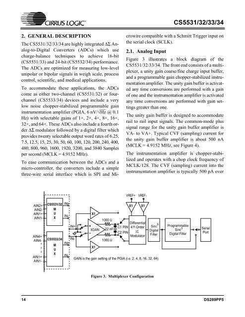
<strong>CS5531</strong>/<strong>32</strong>/<strong>33</strong>/<strong>34</strong>2. GENERAL DESCRIPTIONThe <strong>CS5531</strong>/<strong>32</strong>/<strong>33</strong>/<strong>34</strong> are highly integrated ∆Σ Analog-to-DigitalConverters (ADCs) which usecharge-balance techniques to achieve 16-bit(<strong>CS5531</strong>/<strong>33</strong>) and 24-bit (CS55<strong>32</strong>/<strong>34</strong>) performance.The ADCs are optimized for measuring low-levelunipolar or bipolar signals in weigh scale, processcontrol, scientific, and medical applications.To accommodate these applications, the ADCscome as either two-channel (<strong>CS5531</strong>/<strong>32</strong>) or fourchannel(CS55<strong>33</strong>/<strong>34</strong>) devices and include a verylow noise chopper-stabilized programmable gaininstrumentation amplifier (PGIA, 6 nV/√Hz @0.1Hz) with selectable gains of 1×, 2×, 4×, 8×, 16×,<strong>32</strong>×, and 64×. These ADCs also include a fourth order∆Σ modulator followed by a digital filter whichprovides twenty selectable output word rates of 6.25,7.5, 12.5, 15, 25, 30, 50, 60, 100, 120, 200, 240, 400,480, 800, 960, 1600, 1920, <strong>32</strong>00, and 3840 Samplesper second (MCLK = 4.9152 MHz).To ease communication between the ADCs and amicro-controller, the converters include a simplethree-wire serial interface which is SPI and Microwirecompatible with a Schmitt Trigger input onthe serial clock (SCLK).2.1. Analog InputFigure 3 illustrates a block diagram of the<strong>CS5531</strong>/<strong>32</strong>/<strong>33</strong>/<strong>34</strong>. The front end consists of a multiplexer,a unity gain coarse/fine charge input buffer,and a programmable gain chopper-stabilized instrumentationamplifier. The unity gain buffer is activatedany time conversions are performed with a gainof one and the instrumentation amplifier is activatedany time conversions are performed with gain settingsgreater than one.The unity gain buffer is designed to accommodaterail to rail input signals. The common-mode plussignal range for the unity gain buffer amplifier isVA- to VA+. Typical CVF (sampling) current forthe unity gain buffer amplifier is about 500 nA(MCLK = 4.9152 MHz, see Figure 4).The instrumentation amplifier is chopper-stabilizedand operates with a chop clock frequency ofMCLK/128. The CVF (sampling) current into theinstrumentation amplifier is typically 500 pA overVREF+<strong>CS5531</strong>/<strong>32</strong> IN+X1 X1MUX1XIN-1000 ΩDifferential 5IN+C1 PIN 4 th Order SincXGAIN 22 nFDigitalC2 PIN ∆ΣModulatorFilterCS55<strong>33</strong>/<strong>34</strong> IN-1000 ΩIN+MX1UXIN-GAIN is the gain setting of the PGIA (i.e. 2, 4, 8, 16, <strong>32</strong>, 64)VREF-AIN2+AIN2-AIN1+AIN1-AIN4+AIN4-***AIN1+AIN1-Programmable3SincSerialDigital FilterPortFigure 3. Multiplexer Configuration14 DS289PP5