CS5531/32/33/34 - Eshop-Rychle.cz
CS5531/32/33/34 - Eshop-Rychle.cz
CS5531/32/33/34 - Eshop-Rychle.cz

Create successful ePaper yourself
Turn your PDF publications into a flip-book with our unique Google optimized e-Paper software.
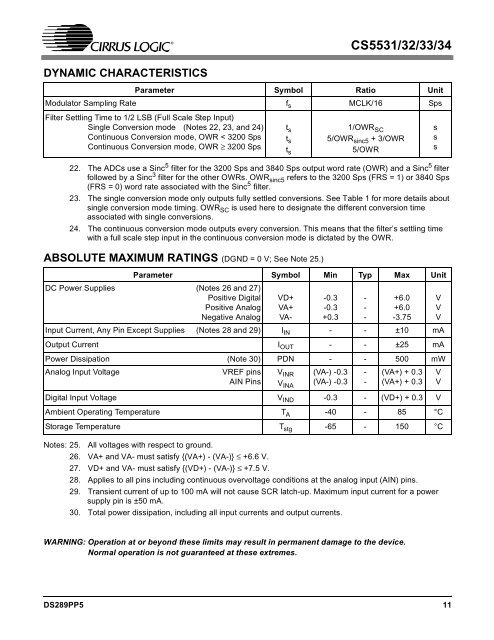
<strong>CS5531</strong>/<strong>32</strong>/<strong>33</strong>/<strong>34</strong>DYNAMIC CHARACTERISTICSParameter Symbol Ratio UnitModulator Sampling Rate f s MCLK/16 SpsFilter Settling Time to 1/2 LSB (Full Scale Step Input)Single Conversion mode (Notes 22, 23, and 24)Continuous Conversion mode, OWR < <strong>32</strong>00 SpsContinuous Conversion mode, OWR ≥ <strong>32</strong>00 Sps22. The ADCs use a Sinc 5 filter for the <strong>32</strong>00 Sps and 3840 Sps output word rate (OWR) and a Sinc 5 filterfollowed by a Sinc 3 filter for the other OWRs. OWR sinc5 refers to the <strong>32</strong>00 Sps (FRS = 1) or 3840 Sps(FRS = 0) word rate associated with the Sinc 5 filter.23. The single conversion mode only outputs fully settled conversions. See Table 1 for more details aboutsingle conversion mode timing. OWR SC is used here to designate the different conversion timeassociated with single conversions.24. The continuous conversion mode outputs every conversion. This means that the filter’s settling timewith a full scale step input in the continuous conversion mode is dictated by the OWR.ABSOLUTE MAXIMUM RATINGS (DGND = 0 V; See Note 25.)Notes: 25. All voltages with respect to ground.26. VA+ and VA- must satisfy {(VA+) - (VA-)} ≤ +6.6 V.27. VD+ and VA- must satisfy {(VD+) - (VA-)} ≤ +7.5 V.28. Applies to all pins including continuous overvoltage conditions at the analog input (AIN) pins.29. Transient current of up to 100 mA will not cause SCR latch-up. Maximum input current for a powersupply pin is ±50 mA.30. Total power dissipation, including all input currents and output currents.t st st s1/OWR SC5/OWR sinc5 +3/OWR5/OWRParameter Symbol Min Typ Max UnitDC Power Supplies (Notes 26 and 27)Positive DigitalPositive AnalogNegative AnalogVD+VA+VA--0.3-0.3+0.3---+6.0+6.0-3.75Input Current, Any Pin Except Supplies (Notes 28 and 29) I IN - - ±10 mAOutput Current I OUT - - ±25 mAPower Dissipation (Note 30) PDN - - 500 mWAnalog Input VoltageVREF pinsAIN PinsV INRV INA(VA-) -0.3(VA-) -0.3--(VA+) + 0.3(VA+) + 0.3VVDigital Input Voltage V IND -0.3 - (VD+) + 0.3 VAmbient Operating Temperature T A -40 - 85 °CStorage Temperature T stg -65 - 150 °CsssVVVWARNING: Operation at or beyond these limits may result in permanent damage to the device.Normal operation is not guaranteed at these extremes.DS289PP5 11