CS5531/32/33/34 - Eshop-Rychle.cz
CS5531/32/33/34 - Eshop-Rychle.cz
CS5531/32/33/34 - Eshop-Rychle.cz

You also want an ePaper? Increase the reach of your titles
YUMPU automatically turns print PDFs into web optimized ePapers that Google loves.
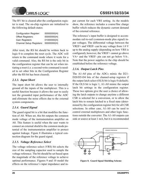
<strong>CS5531</strong>/<strong>32</strong>/<strong>33</strong>/<strong>34</strong>The RV bit is cleared after the configuration registeris read. The on-chip registers are initialized tothe following default states:Configuration Register:Offset Registers:Gain Registers:Channel Setup Registers:After reset, the RS bit should be written back tologic 0 to complete the reset cycle. The ADC willreturn to the command mode where it waits for avalid command. Also, the RS bit is the only bit inthe configuration register that can be set when initiatinga reset (i.e. a second write command is neededto set other bits in the Configuration Registerafter the RS bit has been cleared).2.3.3. Input ShortThe input short bit allows the user to internallyground all the inputs of the multiplexer. This is auseful function because it allows the user to easilytest the grounded input performance of the ADCand eliminate the noise effects due to the externalsystem components.2.3.4. Guard SignalThe guard signal bit is a bit that modifies the functionof A0. When set, this bit outputs the commonmode voltage of the instrumentation amplifier onA0. This feature is useful when the user wants toconnect an external shield to the common mode potentialof the instrumentation amplifier to protectagainst leakage. Figure 8 illustrates a typical connectiondiagram for the guard signal.2.3.5. Voltage Reference Select00000000(H)00000000(H)01000000(H)00000000(H)The voltage reference select (VRS) bit selects thesize of the sampling capacitor used to sample thevoltage reference. The bit should be set based uponthe magnitude of the reference voltage to achieveoptimal performance. Figures 9 and 10 model theeffects on the reference’s input impedance and inputcurrent for each VRS setting. As the modelsshow, the reference includes a coarse/fine chargebuffer which reduces the dynamic current demandof the external reference.The reference’s input buffer is designed to accommodaterail-to-rail (common-mode plus signal) inputvoltages. The differential voltage between theVREF+ and VREF- can be any voltage from 1.0 Vup to the analog supply (depending on how VRS isconfigured), however, the VREF+ cannot go aboveVA+ and the VREF- pin can not go below VA-.Note that the power supplies to the chip should beestablished before the reference voltage.2.3.6. Output Latch PinsThe A1-A0 pins of the ADCs mimic the D21-D20/D5-D4 bits of the channel-setup registers ifthe output latch select (OLS) bit is logic 0 (default).If the OLS bit is logic 1, A1-A0 mimic the outputlatch bit settings in the configuration register.These two options give the user a choice of allowingthe latch outputs to change anytime a differentCSR is selected for a conversion, or to allow thelatch bits to remain latched to a fixed state (determinedby the configuration register bit) for all CSRselections. In either case, A1-A0 can be used tocontrol external multiplexers and other logic functionsoutside the converter. The A1-A0 outputs cansink or source at least 1 mA, but it is recommendedV IN +Com mon Mode = 2.5 VVIN-A0/GUARDAIN+AIN-<strong>CS5531</strong>/<strong>32</strong>/<strong>33</strong>/<strong>34</strong>+5 V A +out pcenterx1out mFigure 8. Guard Signal Shielding Scheme26 DS289PP5