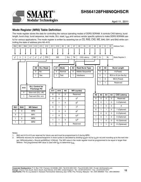
<strong>SH564128FH8N0QHSCR</strong>April 11, 2011Mode Register (MR0) Table DefinitionThe mode register stores the data for controlling the various operating modes of DDR3 SDRAM. It controls CAS latency, burstlength, burst chop, burst sequence, test mode, DLL reset, t WR and various vendor specific options to make DDR3 SDRAM usefulfor various applications. The mode register is written by asserting low on CS, RAS, CAS, WE, BA0, BA1 and BA2 while controllingthe state of address pins A0~A15.BA2 BA1 BA0 A15 A14 A13 A12 A11 A10 A9 A8 A7 A6 A5 A4 A3 A2 A1 A0 Address Field0 1 0 0 0 1 0 1 0 1 PPD WR DLL TM CAS Latency RBT CL BL Mode Register 0A8DLL ResetA7ModeA3Read Burst TypeA1 A0 Burst Length0 No0 Normal0 Nibble Sequential0 0 8 (Fixed)1 Yes1 Test1 Interleave0 1 BC4 or 8 (on-the-fly)1 0 BC4 (Fixed)1 1 ReservedA12DLL Control forPrecharge PD0 Slow exit (DLL off)1 Fast exit (DLL on)BA1 BA0 MR Select0 0 MR00 1 MR11 0 MR21 1 MR3A11 A10 A9 WR (cycles)0 0 0 Reserved0 0 1 5 20 1 0 6 20 1 1 7 21 0 0 8 21 0 1 10 21 1 0 12 21 1 1 ReservedA6 A5 A4 A2 CAS Latency0 0 0 0 Reserved0 0 1 0 5 (Optional)0 1 0 0 60 1 1 0 7 (Optional)1 0 0 0 8 (Optional)1 0 1 0 9 (Optional)1 1 0 0 10 (Optional)1 1 1 0 11 (Optional)Notes:1. BA2 and A13~A15 are reserved for future use and must be programmed to 0 during MRS.2. WR(write recovery for autoprecharge)min in clock cycles is calculated by dividing t WR (in ns) by t CK (in ns) and rounding up to the next integer:WRmin[cycles] = Round-up(tWR[ns] / tCK[ns]). The WR value in the mode register must be programmed to be equal or larger thanWRmin. The programmed WR value is used with t RP to determine t DAL .Corporate Headquarters: P. O. Box 1757, Fremont, CA 94538, USA • Tel:(510) 623-1231 • Fax:(510) 623-1434 • E-mail: info@smartm.comEurope: 5 Kelvin Park South, Kelvin South, East Kilbride, G75 ORH, United Kingdom • Tel: +44-870-870-8747 • Fax: +44-870-870-8757Asia/Pacific: Plot 18, Lrg Jelawat 4, Kawasan Perindustrian Seberang Jaya 13700, Prai, Penang, Malaysia • Tel: +604-3992909 • Fax: +604-399290312
<strong>SH564128FH8N0QHSCR</strong>April 11, 2011Mode Register (MR1) Table DefinitionThe Mode Registers MR1 stores the data for enabling or disabling the DLL, output driver strength, Rtt_Nom impedance, additivelatency, Write Leveling enable, TDQS enable and Qoff. The Mode Register 1 is written by asserting low on CS, RAS, CAS,WE, high on BA0 and low on BA1 and BA2, while controlling the state of address pins A0~A15.BA2 BA1 BA0 A15 A14 A13 A12 A11 A10 A9 A8 A7 A6 A5 A4 A3 A2 A1 A0AddressField0 1 0 1 0 1 0 1 0 1 Qoff TDQS 0 1 Rtt_Nom 0 1 Level Rtt_Nom D.I.C AL Rtt_Nom D.I.C DLLModeRegister 1A11TQDS enableA7Write Leveling enableA4 A3 Additive LatencyA0DLL Enable0 Disabled0 Disabled0 0 0 (AL disabled)0 Enable1 Enabled1 Enabled0 1 CL-11 Disable1 0 CL-21 1 ReservedA12 Qoff 20 Output buffer enabled1 Output buffer disabledBA1 BA0 MR Select0 0 MR00 1 MR11 0 MR21 1 MR3A9 A6 A2 Rtt_Nom 30 0 0 ODT disabled0 0 1 RZQ/40 1 0 RZQ/20 1 1 RZQ/61 0 0 RZQ/12 41 0 1 RZQ/8 41 1 0 Reserved1 1 1 ReservedNote: RZQ = 240ΩA5 A1 Output Driver Impedance Control0 0 Reserved for RZQ/60 1 RZQ/71 0 RZQ/TBD1 1 RZQ/TBDNote: RZQ = 240ΩNotes:1. BA2 and A8, A10, A13~A15 are reserved for future use and must be programmed to 0 during MRS.2. Outputs disabled - DQs, DQSs, DQSs.3. In Write Leveling Mode (MR1[bit7] = 1) with MR1[bit12] = 1, all Rtt_Nom settings are allowed; in Write Leveling Mode (MR1[bit7] =1) withMR1[bit12] = 0, only Rtt_Nom settings of RZQ/2, RZQ/4 and RZQ/6 are allowed.4. If Rtt_Nom is used during Writes, only the values RZQ/2, RZQ/4 and RZQ/6 are allowed.Corporate Headquarters: P. O. Box 1757, Fremont, CA 94538, USA • Tel:(510) 623-1231 • Fax:(510) 623-1434 • E-mail: info@smartm.comEurope: 5 Kelvin Park South, Kelvin South, East Kilbride, G75 ORH, United Kingdom • Tel: +44-870-870-8747 • Fax: +44-870-870-8757Asia/Pacific: Plot 18, Lrg Jelawat 4, Kawasan Perindustrian Seberang Jaya 13700, Prai, Penang, Malaysia • Tel: +604-3992909 • Fax: +604-399290313
- Page 1 and 2: SH564128FH8N0QHSCRApril 11, 2011Ord
- Page 3 and 4: SH564128FH8N0QHSCRApril 11, 20114GB
- Page 5 and 6: SH564128FH8N0QHSCRApril 11, 2011DDR
- Page 7 and 8: SH564128FH8N0QHSCRApril 11, 2011Blo
- Page 9 and 10: SH564128FH8N0QHSCRApril 11, 2011Ser
- Page 11: SH564128FH8N0QHSCRApril 11, 2011Ser
- Page 15 and 16: SH564128FH8N0QHSCRApril 11, 2011Mod
- Page 17 and 18: SH564128FH8N0QHSCRApril 11, 2011Com
- Page 19 and 20: SH564128FH8N0QHSCRApril 11, 2011Abs
- Page 21 and 22: SH564128FH8N0QHSCRApril 11, 2011Inp
- Page 23 and 24: SH564128FH8N0QHSCRApril 11, 2011Sym
- Page 25 and 26: SH564128FH8N0QHSCRApril 11, 2011IDD
- Page 27 and 28: SH564128FH8N0QHSCRApril 11, 2011IDD
- Page 29 and 30: SH564128FH8N0QHSCRApril 11, 2011IDD
- Page 31 and 32: SH564128FH8N0QHSCRApril 11, 2011IDD
- Page 33 and 34: SH564128FH8N0QHSCRApril 11, 2011Ref
- Page 35 and 36: SH564128FH8N0QHSCRApril 11, 2011Dev
- Page 37 and 38: SH564128FH8N0QHSCRApril 11, 2011Par
- Page 39 and 40: SH564128FH8N0QHSCRApril 11, 2011Par
- Page 41 and 42: SH564128FH8N0QHSCRApril 11, 2011aJi
- Page 43: SH564128FH8N0QHSCRApril 11, 2011Dis