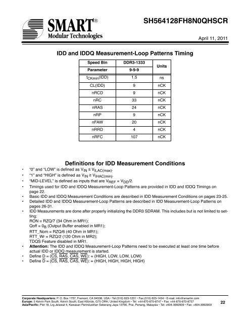
<strong>SH564128FH8N0QHSCR</strong>April 11, 2011IDD and IDDQ Measurement-Loop Patterns TimingSpeed BinDDR3-1333Parameter 9-9-9Unitst CKmin (IDD) 1.5 nsCL(IDD) 9 nCKnRCD 9 nCKnRC 33 nCKnRAS 24 nCKnRP 9 nCKnFAW 20 nCKnRRD 4 nCKnRFC 107 nCKDefinitions for IDD Measurement Conditions• “0” and “LOW” is defined as V IN ≤ V ILAC(max) .• “1” and “HIGH” is defined as V IN ≥ V IHAC(min) .• “MID-LEVEL” is defined as inputs that are V REF = V DD /2.• Timings used for IDD and IDDQ Measurement-Loop Patterns are provided in IDD and IDDQ Timings onpage 22.• Basic IDD and IDDQ Measurement Conditions are described in IDD Measurement Conditions on pages 23-25.• Detailed IDD and IDDQ Measurement-Loop Patterns are described in IDD Measurement-Loop Patterns onpages 26-31.• IDD Measurements are done after properly initializing the DDR3 SDRAM. This includes but is not limited to setting:RON = RZQ/7 (34 Ohm in MR1);Qoff = 0 B (Output Buffer enabled in MR1);RTT_Nom = RZQ/6 (40 Ohm in MR1);RTT_Wr = RZQ/2 (120 Ohm in MR2);TDQS Feature disabled in MR1.• Attention: The IDD and IDDQ Measurement-Loop Patterns need to be executed at least one time beforeactual IDD or IDDQ measurement is started.• Define D = {CS, RAS, CAS, WE}: = {HIGH, LOW, LOW, LOW}• Define D = {CS, RAS, CAS, WE}: = {HIGH, HIGH, HIGH, HIGH}Corporate Headquarters: P. O. Box 1757, Fremont, CA 94538, USA • Tel:(510) 623-1231 • Fax:(510) 623-1434 • E-mail: info@smartm.comEurope: 5 Kelvin Park South, Kelvin South, East Kilbride, G75 ORH, United Kingdom • Tel: +44-870-870-8747 • Fax: +44-870-870-8757Asia/Pacific: Plot 18, Lrg Jelawat 4, Kawasan Perindustrian Seberang Jaya 13700, Prai, Penang, Malaysia • Tel: +604-3992909 • Fax: +604-399290322
<strong>SH564128FH8N0QHSCR</strong>April 11, 2011Symbol Description ConditionsIDD Measurement ConditionsI DD0I DD1I DD2P0I DD2P1I DD2QI DD2NOperating One BankActive-Precharge CurrentOperating One BankActive-Read-PrechargeCurrentPrecharge Power-Down Current SlowExitPrecharge Power-Down Current FastExitPrecharge QuietStandby CurrentPrecharge StandbyCurrentCKE: High; External clock: On; tCK, nRC, nRAS, CL: See IDD and IDDQTimings on page 22; BL: 8 1 ; AL: 0; CS: High between ACT and PRE; Command,Address, Bank Address Inputs: partially toggling according to IDD0Measurement-Loop Pattern on page 26; Data I/O: MID-LEVEL; DM: stableat 0; Bank Activity: Cycling with one bank active at a time: 0,0,1,1,2,2,...(See IDD0 Measurement-Loop Pattern on page 26); Output Buffer and RTT:Enabled in Mode Registers 2 ; ODT Signal: stable at 0; Pattern Details: SeeIDD0 Measurement-Loop Pattern on page 26.CKE: High; External clock: On; tCK, nRC, nRAS, nRCD, CL: See IDD andIDDQ Timings on page 22; BL: 8 1, 6 ; AL: 0; CS: High between ACT, RD andPRE; Command, Address, Bank Address Inputs, Data I/O: partially togglingaccording to IDD1 Measurement-Loop Pattern on page 27; DM: stable at 0;Bank Activity: Cycling with one bank active at a time: 0,0,1,1,2,2,... (SeeIDD1 Measurement-Loop Pattern on page 27); Output Buffer and RTT:Enabled in Mode Registers 2 ; ODT Signal: stable at 0; Pattern Details: SeeIDD1 Measurement-Loop Pattern on page 27.CKE: Low; External clock: On; tCK, CL: See IDD and IDDQ Timings onpage 22; BL: 8 1 ; AL: 0; CS: stable at 1; Command, Address, Bank AddressInputs: stable at 0; Data I/O: MID-LEVEL; DM: stable at 0; Bank Activity: allbanks closed; Output Buffer and RTT: Enabled in Mode Registers 2 ; ODTSignal: stable at 0; Precharge Power Down Mode: Slow Exit 3 .CKE: Low; External clock: On; tCK, CL: See IDD and IDDQ Timings onpage 22; BL: 8 1 ; AL: 0; CS: stable at 1; Command, Address, Bank AddressInputs: stable at 0; Data I/O: MID-LEVEL; DM: stable at 0; Bank Activity: allbanks closed; Output Buffer and RTT: Enabled in Mode Registers 2 ; ODTSignal: stable at 0; Precharge Power Down Mode: Fast Exit 3 .CKE: High; External clock: On; tCK, CL: See IDD and IDDQ Timings onpage 22; BL: 8 1 ; AL: 0; CS: stable at 1; Command, Address, Bank AddressInputs: stable at 0; Data I/O: MID-LEVEL; DM: stable at 0;Bank Activity: allbanks closed; Output Buffer and RTT: Enabled in Mode Registers 2 ; ODTSignal: stable at 0.CKE: High; External clock: On; tCK, CL: See IDD and IDDQ Timings onpage 22; BL: 8 1 ; AL: 0; CS: stable at 1; Command, Address, Bank AddressInputs: partially toggling according to IDD2N and IDD3N Measurement-Loop Pattern on page 28; Data I/O: MID-LEVEL; DM: stable at 0; BankActivity: all banks closed; Output Buffer and RTT: Enabled in ModeRegisters 2 ; ODT Signal: stable at 0; Pattern Details: See IDD2N and IDD3NMeasurement-Loop Pattern on page 28.Corporate Headquarters: P. O. Box 1757, Fremont, CA 94538, USA • Tel:(510) 623-1231 • Fax:(510) 623-1434 • E-mail: info@smartm.comEurope: 5 Kelvin Park South, Kelvin South, East Kilbride, G75 ORH, United Kingdom • Tel: +44-870-870-8747 • Fax: +44-870-870-8757Asia/Pacific: Plot 18, Lrg Jelawat 4, Kawasan Perindustrian Seberang Jaya 13700, Prai, Penang, Malaysia • Tel: +604-3992909 • Fax: +604-399290323
- Page 1 and 2: SH564128FH8N0QHSCRApril 11, 2011Ord
- Page 3 and 4: SH564128FH8N0QHSCRApril 11, 20114GB
- Page 5 and 6: SH564128FH8N0QHSCRApril 11, 2011DDR
- Page 7 and 8: SH564128FH8N0QHSCRApril 11, 2011Blo
- Page 9 and 10: SH564128FH8N0QHSCRApril 11, 2011Ser
- Page 11 and 12: SH564128FH8N0QHSCRApril 11, 2011Ser
- Page 13 and 14: SH564128FH8N0QHSCRApril 11, 2011Mod
- Page 15 and 16: SH564128FH8N0QHSCRApril 11, 2011Mod
- Page 17 and 18: SH564128FH8N0QHSCRApril 11, 2011Com
- Page 19 and 20: SH564128FH8N0QHSCRApril 11, 2011Abs
- Page 21: SH564128FH8N0QHSCRApril 11, 2011Inp
- Page 25 and 26: SH564128FH8N0QHSCRApril 11, 2011IDD
- Page 27 and 28: SH564128FH8N0QHSCRApril 11, 2011IDD
- Page 29 and 30: SH564128FH8N0QHSCRApril 11, 2011IDD
- Page 31 and 32: SH564128FH8N0QHSCRApril 11, 2011IDD
- Page 33 and 34: SH564128FH8N0QHSCRApril 11, 2011Ref
- Page 35 and 36: SH564128FH8N0QHSCRApril 11, 2011Dev
- Page 37 and 38: SH564128FH8N0QHSCRApril 11, 2011Par
- Page 39 and 40: SH564128FH8N0QHSCRApril 11, 2011Par
- Page 41 and 42: SH564128FH8N0QHSCRApril 11, 2011aJi
- Page 43: SH564128FH8N0QHSCRApril 11, 2011Dis