SH564128FH8N0QHSCR - Itautec
SH564128FH8N0QHSCR - Itautec
SH564128FH8N0QHSCR - Itautec
- No tags were found...

Create successful ePaper yourself
Turn your PDF publications into a flip-book with our unique Google optimized e-Paper software.
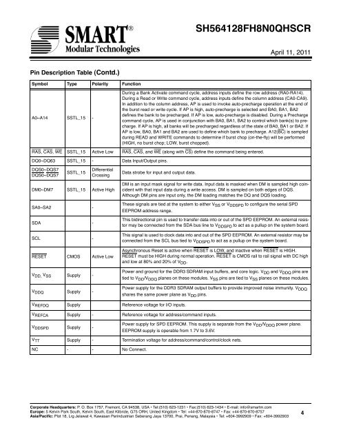
<strong>SH564128FH8N0QHSCR</strong>April 11, 2011Pin Description Table (Contd.)Symbol Type Polarity FunctionA0~A14 SSTL_15 -During a Bank Activate command cycle, address inputs define the row address (RA0-RA14).During a Read or Write command cycle, address inputs define the column address (CA0-CA9).In addition to the column address, AP is used to invoke auto-precharge operation at the end ofthe burst read or write cycle. If AP is high, auto-precharge is selected and BA0, BA1, BA2defines the bank to be precharged. If AP is low, auto-precharge is disabled. During a Prechargecommand cycle, AP is used in conjunction with BA0, BA1, BA2 to control which bank(s) to precharge.If AP is high, all banks will be precharged regardless of the state of BA0, BA1 or BA2. IfAP is low, BA0, BA1 and BA2 are used to define which bank to precharge. A12(BC) is sampledduring READ and WRITE commands to determine if burst chop (on-the-fly) will be performed(HIGH, no burst chop; LOW, burst chopped).RAS, CAS, WE SSTL_15 Active Low RAS, CAS, and WE (along with CS) define the command being entered.DQ0~DQ63 SSTL_15 - Data Input/Output pins.DQS0~DQS7DQS0~DQS7SSTL_15DifferentialCrossingData strobe for input and output data.DM0~DM7 SSTL_15 Active HighSA0~SA2 -SDA -SCL -RESET CMOS Active LowV DD, V SS Supply -V DDQ Supply -DM is an input mask signal for write data. Input data is masked when DM is sampled high coincidentwith that input data during a write access. DM is sampled on both edges of DQS.Although DM pins are input only, the DM loading matches the DQ and DQS loading.These signals are tied at the system to either V SS or V DDSPD to configure the serial SPDEEPROM address range.This bidirectional pin is used to transfer data into or out of the SPD EEPROM. An external resistormay be connected from the SDA bus line to V DDSPD to act as a pullup on the system board.This signal is used to clock data into and out of the SPD EEPROM. An external resistor may beconnected from the SCL bus tied to V DDSPD to act as a pullup on the system board.Asynchronous Reset is active when RESET is LOW, and inactive when RESET is HIGH.RESET must be HIGH during normal operation. RESET is CMOS rail to rail signal with DC highand low at 80% and 20% of V DD .Power and ground for the DDR3 SDRAM input buffers, and core logic. V DD and V DDQ pins aretied to V DD /V DDQ planes on these modules. V SS pins are tied to V SS planes on these modules.Power supply for the DDR3 SDRAM output buffers to provide improved noise immunity. V DDQshares the same power plane as V DD pins.V REFDQ Supply Reference voltage for I/O inputs.V REFCA Supply - Reference voltage for address/command inputs.V DDSPD Supply -Power supply for SPD EEPROM. This supply is separate from the V DD /V DDQ power plane.EEPROM supply is operable from 1.7V to 3.6V.V TT Supply - Termination voltage for address/command/control/clock nets.NC - - No Connect.Corporate Headquarters: P. O. Box 1757, Fremont, CA 94538, USA • Tel:(510) 623-1231 • Fax:(510) 623-1434 • E-mail: info@smartm.comEurope: 5 Kelvin Park South, Kelvin South, East Kilbride, G75 ORH, United Kingdom • Tel: +44-870-870-8747 • Fax: +44-870-870-8757Asia/Pacific: Plot 18, Lrg Jelawat 4, Kawasan Perindustrian Seberang Jaya 13700, Prai, Penang, Malaysia • Tel: +604-3992909 • Fax: +604-39929034