Xilinx 4000-series FPGAs
Xilinx 4000-series FPGAs
Xilinx 4000-series FPGAs

Create successful ePaper yourself
Turn your PDF publications into a flip-book with our unique Google optimized e-Paper software.
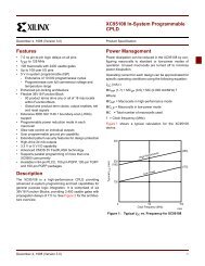
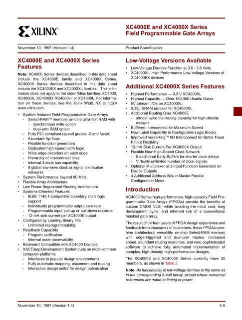
ook1®XC<strong>4000</strong>E and XC<strong>4000</strong>X SeriesField Programmable Gate ArraysNovember 10, 1997 (Version 1.4) 1 4* Product SpecificationXC<strong>4000</strong>E and XC<strong>4000</strong>X SeriesFeaturesNote: XC<strong>4000</strong> Series devices described in this data sheetinclude the XC<strong>4000</strong>E family and XC<strong>4000</strong>X Series.XC<strong>4000</strong>X Series devices described in this data sheetinclude the XC<strong>4000</strong>EX and XC<strong>4000</strong>XL families. This informationdoes not apply to the older <strong>Xilinx</strong> families: XC<strong>4000</strong>,XC<strong>4000</strong>A, XC<strong>4000</strong>D, XC<strong>4000</strong>H, or XC<strong>4000</strong>L. For informationon these devices, see the <strong>Xilinx</strong> WEBLINX at http://www.xilinx.com.• System featured Field-Programmable Gate Arrays- Select-RAM TM memory: on-chip ultra-fast RAM with- synchronous write option- dual-port RAM option- Fully PCI compliant (speed grades -2 and faster)- Abundant flip-flops- Flexible function generators- Dedicated high-speed carry logic- Wide edge decoders on each edge- Hierarchy of interconnect lines- Internal 3-state bus capability- 8 global low-skew clock or signal distributionnetworks• System Performance beyond 80 MHz• Flexible Array Architecture• Low Power Segmented Routing Architecture• Systems-Oriented Features- IEEE 1149.1-compatible boundary scan logicsupport- Individually programmable output slew rate- Programmable input pull-up or pull-down resistors- 12-mA sink current per XC<strong>4000</strong>E output• Configured by Loading Binary File- Unlimited reprogrammability• Readback Capability- Program verification- Internal node observability• Backward Compatible with XC<strong>4000</strong> Devices• XACTstep Development System runs on most commoncomputer platforms- Interfaces to popular design environments- Fully automatic mapping, placement and routing- Interactive design editor for design optimizationLow-Voltage Versions Available• Low-Voltage Devices Function at 3.0 - 3.6 Volts• XC<strong>4000</strong>XL: High Performance Low-Voltage Versions ofXC<strong>4000</strong>EX devicesAdditional XC<strong>4000</strong>X Series Features• Highest Performance — 3.3 V XC<strong>4000</strong>XL• Highest Capacity — Over 180,000 Usable Gates• 5V tolerant I/Os on XC<strong>4000</strong>XL• 0.35µ SRAM process for XC<strong>4000</strong>XL• Additional Routing Over XC<strong>4000</strong>E- almost twice the routing capacity for high-densitydesigns• Buffered Interconnect for Maximum Speed• New Latch Capability in Configurable Logic Blocks• Improved VersaRing TM I/O Interconnect for Better FixedPinout Flexibility• 12-mA Sink Current Per XC<strong>4000</strong>X Output• Flexible New High-Speed Clock Network- 8 additional Early Buffers for shorter clock delays- Virtually unlimited number of clock signals• Optional Multiplexer or 2-input Function Generator onDevice Outputs• 4 Additional Address Bits in Master ParallelConfiguration ModeIntroductionXC<strong>4000</strong> Series high-performance, high-capacity Field ProgrammableGate Arrays (<strong>FPGAs</strong>) provide the benefits ofcustom CMOS VLSI, while avoiding the initial cost, longdevelopment cycle, and inherent risk of a conventionalmasked gate array.The result of thirteen years of FPGA design experience andfeedback from thousands of customers, these <strong>FPGAs</strong> combinearchitectural versatility, on-chip Select-RAM memorywith edge-triggered and dual-port modes, increasedspeed, abundant routing resources, and new, sophisticatedsoftware to achieve fully automated implementation ofcomplex, high-density, high-performance designs.The XC<strong>4000</strong>E and XC<strong>4000</strong>X Series currently have 20members, as shown in Table 2.Note: All functionality in low-voltage families is the same asin the corresponding 5-Volt family, except where numericalreferences are made to timing or power.November 10, 1997 (Version 1.4) 4-5
XC<strong>4000</strong>E and XC<strong>4000</strong>X Series Field Programmable Gate ArraysTable 2: XC<strong>4000</strong>E and XC<strong>4000</strong>X Series Field Programmable Gate ArraysDeviceLogicCellsMax LogicGates(No RAM)Max. RAMBits(No Logic)TypicalGate Range(Logic and RAM)** Max values of Typical Gate Range include 20-30% of CLBs used as RAM.CLBMatrixTotalCLBsNumberofFlip-FlopsMax.User I/OXC4003E 238 3,000 3,200 2,000 - 5,000 10 x 10 100 360 80XC4005E/XL 466 5,000 6,272 3,000 - 9,000 14 x 14 196 616 112XC4006E 608 6,000 8,192 4,000 - 12,000 16 x 16 256 768 128XC4008E 770 8,000 10,368 6,000 - 15,000 18 x 18 324 936 144XC4010E/XL 950 10,000 12,800 7,000 - 20,000 20 x 20 400 1,120 160XC4013E/XL 1368 13,000 18,432 10,000 - 30,000 24 x 24 576 1,536 192XC4020E/XL 1862 20,000 25,088 13,000 - 40,000 28 x 28 784 2,016 224XC4025E 2432 25,000 32,768 15,000 - 45,000 32 x 32 1,024 2,560 256XC4028EX/XL 2432 28,000 32,768 18,000 - 50,000 32 x 32 1,024 2,560 256XC4036EX/XL 3078 36,000 41,472 22,000 - 65,000 36 x 36 1,296 3,168 288XC4044XL 3800 44,000 51,200 27,000 - 80,000 40 x 40 1,600 3,840 320XC4052XL 4598 52,000 61,952 33,000 - 100,000 44 x 44 1,936 4,576 352XC4062XL 5472 62,000 73,728 40,000 - 130,000 48 x 48 2,304 5,376 384XC4085XL 7448 85,000 100,352 55,000 - 180,000 56 x 56 3,136 7,168 448DescriptionXC<strong>4000</strong> Series devices are implemented with a regular,flexible, programmable architecture of Configurable LogicBlocks (CLBs), interconnected by a powerful hierarchy ofversatile routing resources, and surrounded by a perimeterof programmable Input/Output Blocks (IOBs). They havegenerous routing resources to accommodate the mostcomplex interconnect patterns.The devices are customized by loading configuration datainto internal memory cells. The FPGA can either activelyread its configuration data from an external serial or byteparallelPROM (master modes), or the configuration datacan be written into the FPGA from an external device (slaveand peripheral modes).XC<strong>4000</strong> Series <strong>FPGAs</strong> are supported by powerful andsophisticated software, covering every aspect of designfrom schematic or behavioral entry, floorplanning, simulation,automatic block placement and routing of interconnects,to the creation, downloading, and readback of theconfiguration bit stream.Because <strong>Xilinx</strong> <strong>FPGAs</strong> can be reprogrammed an unlimitednumber of times, they can be used in innovative designswhere hardware is changed dynamically, or where hardwaremust be adapted to different user applications.<strong>FPGAs</strong> are ideal for shortening design and developmentcycles, and also offer a cost-effective solution for productionrates well beyond 5,000 systems per month. For lowesthigh-volume unit cost, a design can first be implemented inthe XC<strong>4000</strong>E or XC<strong>4000</strong>X, then migrated to one of <strong>Xilinx</strong>’compatible HardWire mask-programmed devices.Taking Advantage of ReconfigurationFPGA devices can be reconfigured to change logic functionwhile resident in the system. This capability gives the systemdesigner a new degree of freedom not available withany other type of logic.Hardware can be changed as easily as software. Designupdates or modifications are easy, and can be made toproducts already in the field. An FPGA can even be reconfigureddynamically to perform different functions at differenttimes.Reconfigurable logic can be used to implement systemself-diagnostics, create systems capable of being reconfiguredfor different environments or operations, or implementmulti-purpose hardware for a given application. As anadded benefit, using reconfigurable FPGA devices simplifieshardware design and debugging and shortens producttime-to-market.4-6 November 10, 1997 (Version 1.4)
XC<strong>4000</strong>E and XC<strong>4000</strong>X SeriesCompared to the XC<strong>4000</strong>For readers already familiar with the XC<strong>4000</strong> family of <strong>Xilinx</strong>Field Programmable Gate Arrays, the major new featuresin the XC<strong>4000</strong> Series devices are listed in thissection. The biggest advantages of XC<strong>4000</strong>E andXC<strong>4000</strong>X devices are significantly increased systemspeed, greater capacity, and new architectural features,particularly Select-RAM memory. The XC<strong>4000</strong>X devicesalso offer many new routing features, including specialhigh-speed clock buffers that can be used to capture inputdata with minimal delay.Any XC<strong>4000</strong>E device is pinout- and bitstream-compatiblewith the corresponding XC<strong>4000</strong> device. An existingXC<strong>4000</strong> bitstream can be used to program an XC<strong>4000</strong>Edevice. However, since the XC<strong>4000</strong>E includes many newfeatures, an XC<strong>4000</strong>E bitstream cannot be loaded into anXC<strong>4000</strong> device.XC<strong>4000</strong>X Series devices are not bitstream-compatible withequivalent array size devices in the XC<strong>4000</strong> or XC<strong>4000</strong>Efamilies. However, equivalent array size devices, such asthe XC4025, XC4025E, XC4028EX, and XC4028XL, arepinout-compatible.Improvements in XC<strong>4000</strong>E and XC<strong>4000</strong>XIncreased System SpeedXC<strong>4000</strong>E and XC<strong>4000</strong>X devices can run at synchronoussystem clock rates of up to 80 MHz, and internal performancecan exceed 150 MHz. This increase in performanceover the previous families stems from improvements in bothdevice processing and system architecture. XC<strong>4000</strong>Series devices use a sub-micron multi-layer metal process.In addition, many architectural improvements have beenmade, as described below.The XC<strong>4000</strong>XL family is a high performance 3.3V familybased on 0.35µ SRAM technology and supports systemspeeds to 80 MHz.PCI ComplianceXC<strong>4000</strong> Series -2 and faster speed grades are fully PCIcompliant. XC<strong>4000</strong>E and XC<strong>4000</strong>X devices can be used toimplement a one-chip PCI solution.Carry LogicThe speed of the carry logic chain has increased dramatically.Some parameters, such as the delay on the carrychain through a single CLB (TBYP), have improved by asmuch as 50% from XC<strong>4000</strong> values. See “Fast Carry Logic”on page 4-18 for more information.Select-RAM Memory: Edge-Triggered, SynchronousRAM ModesThe RAM in any CLB can be configured for synchronous,edge-triggered, write operation. The read operation is notaffected by this change to an edge-triggered write.Dual-Port RAMA separate option converts the 16x2 RAM in any CLB into a16x1 dual-port RAM with simultaneous Read/Write.The function generators in each CLB can be configured aseither level-sensitive (asynchronous) single-port RAM,edge-triggered (synchronous) single-port RAM, edge-triggered(synchronous) dual-port RAM, or as combinatoriallogic.Configurable RAM ContentThe RAM content can now be loaded at configuration time,so that the RAM starts up with user-defined data.H Function GeneratorIn current XC<strong>4000</strong> Series devices, the H function generatoris more versatile than in the original XC<strong>4000</strong>. Its inputs cancome not only from the F and G function generators butalso from up to three of the four control input lines. The Hfunction generator can thus be totally or partially independentof the other two function generators, increasing themaximum capacity of the device.IOB Clock EnableThe two flip-flops in each IOB have a common clock enableinput, which through configuration can be activated individuallyfor the input or output flip-flop or both. This clockenable operates exactly like the EC pin on the XC<strong>4000</strong>CLB. This new feature makes the IOBs more versatile, andavoids the need for clock gating.Output DriversThe output pull-up structure defaults to a TTL-like totempole.This driver is an n-channel pull-up transistor, pulling toa voltage one transistor threshold below Vcc, just like theXC<strong>4000</strong> family outputs. Alternatively, XC<strong>4000</strong> Seriesdevices can be globally configured with CMOS outputs,with p-channel pull-up transistors pulling to Vcc. Also, theconfigurable pull-up resistor in the XC<strong>4000</strong> Series is a p-channel transistor that pulls to Vcc, whereas in the originalXC<strong>4000</strong> family it is an n-channel transistor that pulls to avoltage one transistor threshold below Vcc.November 10, 1997 (Version 1.4) 4-7
XC<strong>4000</strong>E and XC<strong>4000</strong>X Series Field Programmable Gate ArraysInput ThresholdsThe input thresholds of 5V devices can be globally configuredfor either TTL (1.2 V threshold) or CMOS (2.5 Vthreshold), just like XC2000 and XC3000 inputs. The twoglobal adjustments of input threshold and output level areindependent of each other. The XC<strong>4000</strong>XL family has aninput threshold of 1.6V, compatible with both 3.3V CMOSand TTL levels.Global Signal Access to LogicThere is additional access from global clocks to the F andG function generator inputs.Configuration Pin Pull-Up ResistorsDuring configuration, the three mode pins, M0, M1, andM2, have weak pull-up resistors. For the most popular configurationmode, Slave Serial, the mode pins can thus beleft unconnected.The three mode inputs can be individually configured withor without weak pull-up or pull-down resistors after configuration.The PROGRAM input pin has a permanent weak pull-up.Soft Start-upLike the XC3000A, XC<strong>4000</strong> Series devices have “SoftStart-up.” When the configuration process is finished andthe device starts up, the first activation of the outputs isautomatically slew-rate limited. This feature avoids potentialground bounce when all outputs are turned on simultaneously.Immediately after start-up, the slew rate of theindividual outputs is, as in the XC<strong>4000</strong> family, determinedby the individual configuration option.XC<strong>4000</strong> and XC<strong>4000</strong>A CompatibilityExisting XC<strong>4000</strong> bitstreams can be used to configure anXC<strong>4000</strong>E device. XC<strong>4000</strong>A bitstreams must be recompiledfor use with the XC<strong>4000</strong>E due to improved routingresources, although the devices are pin-for-pin compatible.Additional Improvements in XC<strong>4000</strong>X OnlyIncreased RoutingNew interconnect in the XC<strong>4000</strong>X includes twenty-twoadditional vertical lines in each column of CLBs and twelvenew horizontal lines in each row of CLBs. The twelve “QuadLines” in each CLB row and column include optional repoweringbuffers for maximum speed. Additional high-performancerouting near the IOBs enhances pin flexibility.Faster Input and OutputA fast, dedicated early clock sourced by global clock buffersis available for the IOBs. To ensure synchronization with theregular global clocks, a Fast Capture latch driven by theearly clock is available. The input data can be initiallyloaded into the Fast Capture latch with the early clock, thentransferred to the input flip-flop or latch with the low-skewglobal clock. A programmable delay on the input can beused to avoid hold-time requirements. See “IOB Input Signals”on page 4-21 for more information.Latch Capability in CLBsStorage elements in the XC<strong>4000</strong>X CLB can be configuredas either flip-flops or latches. This capability makes theFPGA highly synthesis-compatible.IOB Output MUX From Output ClockA multiplexer in the IOB allows the output clock to selecteither the output data or the IOB clock enable as the outputto the pad. Thus, two different data signals can share a singleoutput pad, effectively doubling the number of deviceoutputs without requiring a larger, more expensive package.This multiplexer can also be configured as an ANDgateto implement a very fast pin-to-pin path. See “IOB OutputSignals” on page 4-24 for more information.Additional Address BitsLarger devices require more bits of configuration data. Adaisy chain of several large XC<strong>4000</strong>X devices may requirea PROM that cannot be addressed by the eighteen addressbits supported in the XC<strong>4000</strong>E. The XC<strong>4000</strong>X Seriestherefore extends the addressing in Master Parallel configurationmode to 22 bits.4-8 November 10, 1997 (Version 1.4)
Detailed Functional DescriptionXC<strong>4000</strong> Series devices achieve high speed throughadvanced semiconductor technology and improved architecture.The XC<strong>4000</strong>E and XC<strong>4000</strong>X support system clockrates of up to 80 MHz and internal performance in excessof 150 MHz. Compared to older <strong>Xilinx</strong> FPGA families,XC<strong>4000</strong> Series devices are more powerful. They offer onchipedge-triggered and dual-port RAM, clock enables on I/O flip-flops, and wide-input decoders. They are more versatilein many applications, especially those involving RAM.Design cycles are faster due to a combination of increasedrouting resources and more sophisticated software.Basic Building Blocks<strong>Xilinx</strong> user-programmable gate arrays include two majorconfigurable elements: configurable logic blocks (CLBs)and input/output blocks (IOBs).• CLBs provide the functional elements for constructingthe user’s logic.• IOBs provide the interface between the package pinsand internal signal lines.Three other types of circuits are also available:• 3-State buffers (TBUFs) driving horizontal longlines areassociated with each CLB.• Wide edge decoders are available around the peripheryof each device.• An on-chip oscillator is provided.Programmable interconnect resources provide routingpaths to connect the inputs and outputs of these configurableelements to the appropriate networks.The functionality of each circuit block is customized duringconfiguration by programming internal static memory cells.The values stored in these memory cells determine thelogic functions and interconnections implemented in theFPGA. Each of these available circuits is described in thissection.Configurable Logic Blocks (CLBs)Configurable Logic Blocks implement most of the logic inan FPGA. The principal CLB elements are shown inFigure 2. Two 4-input function generators (F and G) offerunrestricted versatility. Most combinatorial logic functionsneed four or fewer inputs. However, a third function generator(H) is provided. The H function generator has threeinputs. Either zero, one, or two of these inputs can be theoutputs of F and G; the other input(s) are from outside theCLB. The CLB can, therefore, implement certain functionsof up to nine variables, like parity check or expandableidentitycomparison of two sets of four inputs.Each CLB contains two storage elements that can be usedto store the function generator outputs. However, the storageelements and function generators can also be usedindependently. These storage elements can be configuredas flip-flops in both XC<strong>4000</strong>E and XC<strong>4000</strong>X devices; in theXC<strong>4000</strong>X they can optionally be configured as latches. DINcan be used as a direct input to either of the two storageelements. H1 can drive the other through the H functiongenerator. Function generator outputs can also drive twooutputs independent of the storage element outputs. Thisversatility increases logic capacity and simplifies routing.Thirteen CLB inputs and four CLB outputs provide accessto the function generators and storage elements. Theseinputs and outputs connect to the programmable interconnectresources outside the block.Function GeneratorsFour independent inputs are provided to each of two functiongenerators (F1 - F4 and G1 - G4). These function generators,with outputs labeled F’ and G’, are each capable ofimplementing any arbitrarily defined Boolean function offour inputs. The function generators are implemented asmemory look-up tables. The propagation delay is thereforeindependent of the function implemented.A third function generator, labeled H’, can implement anyBoolean function of its three inputs. Two of these inputs canoptionally be the F’ and G’ functional generator outputs.Alternatively, one or both of these inputs can come fromoutside the CLB (H2, H0). The third input must come fromoutside the block (H1).Signals from the function generators can exit the CLB ontwo outputs. F’ or H’ can be connected to the X output. G’ orH’ can be connected to the Y output.A CLB can be used to implement any of the following functions:• any function of up to four variables, plus any secondfunction of up to four unrelated variables, plus any thirdfunction of up to three unrelated variables 1• any single function of five variables• any function of four variables together with somefunctions of six variables• some functions of up to nine variables.Implementing wide functions in a single block reduces boththe number of blocks required and the delay in the signalpath, achieving both increased capacity and speed.The versatility of the CLB function generators significantlyimproves system speed. In addition, the design-softwaretools can deal with each function generator independently.This flexibility improves cell usage.1. When three separate functions are generated, one of the function outputs must be captured in a flip-flop internal to the CLB. Only twounregistered function generator outputs are available from the CLB.November 10, 1997 (Version 1.4) 4-9
XC<strong>4000</strong>E and XC<strong>4000</strong>X Series Field Programmable Gate ArraysC 1 • • • C 44H 1 D IN /H 2 SR/H0 ECG 4G 3G 2LOGICFUNCTIONG'OFG1-G4DINF'G'H'S/RCONTROLDSDQBypassYQG 1LOGICFUNCTIONOFH'F', G',ANDH1G'H'1YECRDBypassF 4F 3F 2LOGICFUNCTIONOFF1-F4F'DINF'G'H'S/RCONTROLDSDQXQF 1K(CLOCK)H'F'1ECRDXMultiplexer Controlledby Configuration ProgramX6692Figure 2: Simplified Block Diagram of XC<strong>4000</strong> Series CLB (RAM and Carry Logic functions not shown)Flip-FlopsThe CLB can pass the combinatorial output(s) to the interconnectnetwork, but can also store the combinatorialresults or other incoming data in one or two flip-flops, andconnect their outputs to the interconnect network as well.The two edge-triggered D-type flip-flops have commonclock (K) and clock enable (EC) inputs. Either or both clockinputs can also be permanently enabled. Storage elementfunctionality is described in Table 3.Latches (XC<strong>4000</strong>X only)The CLB storage elements can also be configured aslatches. The two latches have common clock (K) and clockenable (EC) inputs. Storage element functionality isdescribed in Table 3.Clock InputEach flip-flop can be triggered on either the rising or fallingclock edge. The clock pin is shared by both storage elements.However, the clock is individually invertible for eachstorage element. Any inverter placed on the clock input isautomatically absorbed into the CLB.Clock EnableThe clock enable signal (EC) is active High. The EC pin isshared by both storage elements. If left unconnected foreither, the clock enable for that storage element defaults tothe active state. EC is not invertible within the CLB.Table 3: CLB Storage Element Functionality(active rising edge is shown)Mode K EC SR D QPower-Up orGSRX X X X SRX X 1 X SRFlip-Flop __/ 1* 0* D D0 X 0* X QLatch1 1* 0* X Q0 1* 0* D DBoth X 0 0* X QLegend:X__/SR0*1*Don’t careRising edgeSet or Reset value. Reset is default.Input is Low or unconnected (default value)Input is High or unconnected (default value)4-10 November 10, 1997 (Version 1.4)
XC<strong>4000</strong>E and XC<strong>4000</strong>X Series Field Programmable Gate ArraysSupported CLB memory configurations and timing modesfor single- and dual-port modes are shown in Table 4.XC<strong>4000</strong> Series devices are the first programmable logicdevices with edge-triggered (synchronous) and dual-portRAM accessible to the user. Edge-triggered RAM simplifiessystem timing. Dual-port RAM doubles the effectivethroughput of FIFO applications. These features can beindividually programmed in any XC<strong>4000</strong> Series CLB.Advantages of On-Chip and Edge-Triggered RAMThe on-chip RAM is extremely fast. The read access time isthe same as the logic delay. The write access time isslightly slower. Both access times are much faster thanany off-chip solution, because they avoid I/O delays.Edge-triggered RAM, also called synchronous RAM, is afeature never before available in a Field ProgrammableGate Array. The simplicity of designing with edge-triggeredRAM, and the markedly higher achievable performance,add up to a significant improvement over existing deviceswith on-chip RAM.Three application notes are available from <strong>Xilinx</strong> that discussedge-triggered RAM: “XC<strong>4000</strong>E Edge-Triggered andDual-Port RAM Capability,” “Implementing FIFOs inXC<strong>4000</strong>E RAM,” and “Synchronous and AsynchronousFIFO Designs.” All three application notes apply to bothXC<strong>4000</strong>E and XC<strong>4000</strong>X RAM.Table 4: Supported RAM Modes16x116x232x1RAM Inputs and OutputsThe F1-F4 and G1-G4 inputs to the function generators actas address lines, selecting a particular memory cell in eachlook-up table.The functionality of the CLB control signals changes whenthe function generators are configured as RAM. The DIN/H2, H1, and SR/H0 lines become the two data inputs (D0,D1) and the Write Enable (WE) input for the 16x2 memory.When the 32x1 configuration is selected, D1 acts as thefifth address bit and D0 is the data input.The contents of the memory cell(s) being addressed areavailable at the F’ and G’ function-generator outputs. Theycan exit the CLB through its X and Y outputs, or can be capturedin the CLB flip-flop(s).Configuring the CLB function generators as Read/Writememory does not affect the functionality of the other por-Edge-TriggeredTimingLevel-SensitiveTimingSingle-Port √ √ √ √ √Dual-Port √ √RAM Configuration OptionsThe function generators in any CLB can be configured asRAM arrays in the following sizes:• Two 16x1 RAMs: two data inputs and two data outputswith identical or, if preferred, different addressing foreach RAM• One 32x1 RAM: one data input and one data output.One F or G function generator can be configured as a 16x1RAM while the other function generators are used to implementany function of up to 5 inputs.Additionally, the XC<strong>4000</strong> Series RAM may have either oftwo timing modes:• Edge-Triggered (Synchronous): data written by thedesignated edge of the CLB clock. WE acts as a trueclock enable.• Level-Sensitive (Asynchronous): an external WE signalacts as the write strobe.The selected timing mode applies to both function generatorswithin a CLB when both are configured as RAM.The number of read ports is also programmable:• Single Port: each function generator has a commonread and write port• Dual Port: both function generators are configuredtogether as a single 16x1 dual-port RAM with one writeport and two read ports. Simultaneous read and writeoperations to the same or different addresses aresupported.RAM configuration options are selected by placing theappropriate library symbol.Choosing a RAM Configuration ModeThe appropriate choice of RAM mode for a given designshould be based on timing and resource requirements,desired functionality, and the simplicity of the design process.Recommended usage is shown in Table 5.The difference between level-sensitive, edge-triggered,and dual-port RAM is only in the write operation. Readoperation and timing is identical for all modes of operation.Table 5: RAM Mode SelectionUse for NewDesigns?Size (16x1,Registered)SimultaneousRead/WriteRelativePerformanceLevel-SensitiveEdge-TriggeredDual-PortEdge-TriggeredNo Yes Yes1/2 CLB 1/2 CLB 1 CLBNo No YesX2X2X (4Xeffective)4-12 November 10, 1997 (Version 1.4)
tions of the CLB, with the exception of the redefinition of thecontrol signals. In 16x2 and 16x1 modes, the H’ functiongenerator can be used to implement Boolean functions ofF’, G’, and D1, and the D flip-flops can latch the F’, G’, H’, orD0 signals.Single-Port Edge-Triggered ModeEdge-triggered (synchronous) RAM simplifies timingrequirements. XC<strong>4000</strong> Series edge-triggered RAM timingoperates like writing to a data register. Data and addressare presented. The register is enabled for writing by a logicHigh on the write enable input, WE. Then a rising or fallingclock edge loads the data into the register, as shown inFigure 4.WCLK (K)T WPSComplex timing relationships between address, data, andwrite enable signals are not required, and the external writeenable pulse becomes a simple clock enable. The activeedge of WCLK latches the address, input data, and WE signals.An internal write pulse is generated that performs thewrite. See Figure 5 and Figure 6 for block diagrams of aCLB configured as 16x2 and 32x1 edge-triggered, singleportRAM.The relationships between CLB pins and RAM inputs andoutputs for single-port, edge-triggered mode are shown inTable 6.The Write Clock input (WCLK) can be configured as activeon either the rising edge (default) or the falling edge. It usesthe same CLB pin (K) used to clock the CLB flip-flops, but itcan be independently inverted. Consequently, the RAMoutput can optionally be registered within the same CLBeither by the same clock edge as the RAM, or by the oppositeedge of this clock. The sense of WCLK applies to bothfunction generators in the CLB when both are configuredas RAM.WEDATA INADDRESST WSST DSST ASST WHST DHST AHSThe WE pin is active-High and is not invertible within theCLB.Note: The pulse following the active edge of WCLK (T WPSin Figure 4) must be less than one millisecond wide. Formost applications, this requirement is not overly restrictive;however, it must not be forgotten. Stopping WCLK at thispoint in the write cycle could result in excessive current andeven damage to the larger devices if many CLBs are configuredas edge-triggered RAM.Table 6: Single-Port Edge-Triggered RAM SignalsT ILOT WOST ILODATA OUT OLD NEWFigure 4:Edge-Triggered RAM Write TimingX6461RAM Signal CLB Pin FunctionDD0 or D1 (16x2, Data In16x1), D0 (32x1)A[3:0] F1-F4 or G1-G4 AddressA[4] D1 (32x1) AddressWE WE Write EnableWCLK K ClockSPO(Data Out)F’ or G’ Single Port Out(Data Out)November 10, 1997 (Version 1.4) 4-13
XC<strong>4000</strong>E and XC<strong>4000</strong>X Series Field Programmable Gate ArraysC 1 • • • C 44WE D 1D 0ECD ING 1 • • • G 444WRITEDECODER1 of 1616-LATCHARRAYMUXG'LATCHENABLEWRITE PULSEREADADDRESSD INF 1 • • • F 44 4WRITEDECODER1 of 1616-LATCHARRAYMUXF'K(CLOCK)LATCHENABLEWRITE PULSEREADADDRESSFigure 5:16x2 (or 16x1) Edge-Triggered Single-Port RAMX6752C 1 • • • C 44WE D 1/A 4D 0ECECD ING 1 • • • G 4F 1 • • • F 444WRITEDECODER1 of 1616-LATCHARRAYMUXG'LATCHENABLEWRITE PULSEREADADDRESSH'D IN4 4WRITEDECODER1 of 1616-LATCHARRAYMUXF'K(CLOCK)LATCHENABLEWRITE PULSEREADADDRESSX6754Figure 6: 32x1 Edge-Triggered Single-Port RAM (F and G addresses are identical)4-14 November 10, 1997 (Version 1.4)
Dual-Port Edge-Triggered ModeIn dual-port mode, both the F and G function generatorsare used to create a single 16x1 RAM array with one writeport and two read ports. The resulting RAM array can beread and written simultaneously at two independentaddresses. Simultaneous read and write operations at thesame address are also supported.Dual-port mode always has edge-triggered write timing, asshown in Figure 4.Figure 7 shows a simple model of an XC<strong>4000</strong> Series CLBconfigured as dual-port RAM. One address port, labeledA[3:0], supplies both the read and write address for the Ffunction generator. This function generator behaves thesame as a 16x1 single-port edge-triggered RAM array. TheRAM output, Single Port Out (SPO), appears at the F functiongenerator output. SPO, therefore, reflects the data ataddress A[3:0].The other address port, labeled DPRA[3:0] for Dual PortRead Address, supplies the read address for the G functiongenerator. The write address for the G function generator,however, comes from the address A[3:0]. The output fromthis 16x1 RAM array, Dual Port Out (DPO), appears at theG function generator output. DPO, therefore, reflects thedata at address DPRA[3:0].Therefore, by using A[3:0] for the write address andDPRA[3:0] for the read address, and reading only the DPOoutput, a FIFO that can read and write simultaneously iseasily generated. Simultaneous access doubles the effectivethroughput of the FIFO.The relationships between CLB pins and RAM inputs andoutputs for dual-port, edge-triggered mode are shown inTable 7. See Figure 8 on page 4-16 for a block diagram of aCLB configured in this mode.WEDDPRA[3:0]A[3:0]WCLKRAM16X1D PrimitiveWED D QAR[3:0]AW[3:0]G Function GeneratorWEDAR[3:0]AW[3:0]F Function GeneratorDQDPO (Dual Port Out)Registered DPOSPO (Single Port Out)Registered SPOFigure 7: XC<strong>4000</strong> Series Dual-Port RAM, SimpleModelX6755Table 7: Dual-Port Edge-Triggered RAM SignalsRAM Signal CLB Pin FunctionD D0 Data InA[3:0] F1-F4 Read Address for F,Write Address for F and GDPRA[3:0] G1-G4 Read Address for GWE WE Write EnableWCLK K ClockSPO F’ Single Port Out(addressed by A[3:0])DPO G’ Dual Port Out(addressed by DPRA[3:0])Note: The pulse following the active edge of WCLK (T WPSin Figure 4) must be less than one millisecond wide. Formost applications, this requirement is not overly restrictive;however, it must not be forgotten. Stopping WCLK at thispoint in the write cycle could result in excessive current andeven damage to the larger devices if many CLBs are configuredas edge-triggered RAM.Single-Port Level-Sensitive Timing ModeNote: Edge-triggered mode is recommended for all newdesigns. Level-sensitive mode, also called asynchronousmode, is still supported for XC<strong>4000</strong> Series backward-compatibilitywith the XC<strong>4000</strong> family.Level-sensitive RAM timing is simple in concept but can becomplicated in execution. Data and address signals arepresented, then a positive pulse on the write enable pin(WE) performs a write into the RAM at the designatedaddress. As indicated by the “level-sensitive” label, thisRAM acts like a latch. During the WE High pulse, changingthe data lines results in new data written to the old address.Changing the address lines while WE is High results in spuriousdata written to the new address—and possibly atother addresses as well, as the address lines inevitably donot all change simultaneously.The user must generate a carefully timed WE signal. Thedelay on the WE signal and the address lines must be carefullyverified to ensure that WE does not become activeuntil after the address lines have settled, and that WE goesinactive before the address lines change again. The datamust be stable before and after the falling edge of WE.In practical terms, WE is usually generated by a 2X clock. Ifa 2X clock is not available, the falling edge of the systemclock can be used. However, there are inherent risks in thisapproach, since the WE pulse must be guaranteed inactivebefore the next rising edge of the system clock. Severalolder application notes are available from <strong>Xilinx</strong> that discussthe design of level-sensitive RAMs. These applicationnotes include XAPP031, “Using the XC<strong>4000</strong> RAM Capability,”and XAPP042, “High-Speed RAM Design in XC<strong>4000</strong>.”However, the edge-triggered RAM available in the XC<strong>4000</strong>Series is superior to level-sensitive RAM for almost everyapplication.November 10, 1997 (Version 1.4) 4-15
XC<strong>4000</strong>E and XC<strong>4000</strong>X Series Field Programmable Gate ArraysC 1 • • • C 44WE D 1D 0ECD IN4WRITEDECODER1 of 1616-LATCHARRAYMUXG'LATCHENABLEG1 • • • G44WRITE PULSEREADADDRESSD INF1 • • • F44 4WRITEDECODER1 of 1616-LATCHARRAYMUXF'K(CLOCK)LATCHENABLEWRITE PULSEREADADDRESSX6748Figure 8: 16x1 Edge-Triggered Dual-Port RAMFigure 9 shows the write timing for level-sensitive, singleportRAM.The relationships between CLB pins and RAM inputs andoutputs for single-port level-sensitive mode are shown inTable 8.Figure 10 and Figure 11 show block diagrams of a CLBconfigured as 16x2 and 32x1 level-sensitive, single-portRAM.Initializing RAM at ConfigurationBoth RAM and ROM implementations of the XC<strong>4000</strong>Series devices are initialized during configuration. The initialcontents are defined via an INIT attribute or propertyattached to the RAM or ROM symbol, as described in theschematic library guide. If not defined, all RAM contentsare initialized to all zeros, by default.RAM initialization occurs only during configuration. TheRAM content is not affected by Global Set/Reset.Table 8: Single-Port Level-Sensitive RAM SignalsRAM Signal CLB Pin FunctionD D0 or D1 Data InA[3:0] F1-F4 or G1-G4 AddressWE WE Write EnableO F’ or G’ Data Out4-16 November 10, 1997 (Version 1.4)
T WCADDRESSTASTWPT AHWRITE ENABLETDSTDHDATA INREQUIREDFigure 9: Level-Sensitive RAM Write TimingX6462C 1 • • • C 44WE D 1 D 0ECEnableD ING 1 • • • G 44WRITEDECODER1 of 1616-LATCHARRAYMUXG'4READ ADDRESSEnableD INF 1 • • • F 44WRITEDECODER1 of 1616-LATCHARRAYMUXF'X67464READ ADDRESSFigure 10: 16x2 (or 16x1) Level-Sensitive Single-Port RAMNovember 10, 1997 (Version 1.4) 4-17
XC<strong>4000</strong>E and XC<strong>4000</strong>X Series Field Programmable Gate ArraysC 1 • • • C 44WE D 1 /A 4 D 0ECEnableDING 1 • • • G 4F 1 • • • F 44WRITEDECODER1 of 1616-LATCHARRAYMUXG'4READ ADDRESSH'EnableDIN4WRITEDECODER1 of 1616-LATCHARRAYMUXF'4READ ADDRESSX6749Figure 11: 32x1 Level-Sensitive Single-Port RAM (F and G addresses are identical)Fast Carry LogicEach CLB F and G function generator contains dedicatedarithmetic logic for the fast generation of carry and borrowsignals. This extra output is passed on to the function generatorin the adjacent CLB. The carry chain is independentof normal routing resources.Dedicated fast carry logic greatly increases the efficiencyand performance of adders, subtractors, accumulators,comparators and counters. It also opens the door to manynew applications involving arithmetic operation, where theprevious generations of <strong>FPGAs</strong> were not fast enough or tooinefficient. High-speed address offset calculations in microprocessoror graphics systems, and high-speed addition indigital signal processing are two typical applications.The two 4-input function generators can be configured as a2-bit adder with built-in hidden carry that can be expandedto any length. This dedicated carry circuitry is so fast andefficient that conventional speed-up methods like carrygenerate/propagate are meaningless even at the 16-bitlevel, and of marginal benefit at the 32-bit level.This fast carry logic is one of the more significant featuresof the XC<strong>4000</strong> Series, speeding up arithmetic and countinginto the 70 MHz range.The carry chain in XC<strong>4000</strong>E devices can run either up ordown. At the top and bottom of the columns where thereare no CLBs above and below, the carry is propagated tothe right. (See Figure 12.) In order to improve speed in thehigh-capacity XC<strong>4000</strong>X devices, which can potentiallyhave very long carry chains, the carry chain travels upwardonly, as shown in Figure 13. Additionally, standard interconnectcan be used to route a carry signal in the downwarddirection.Figure 14 on page 4-20 shows an XC<strong>4000</strong>E CLB with dedicatedfast carry logic. The carry logic in the XC<strong>4000</strong>X issimilar, except that COUT exits at the top only, and the signalCINDOWN does not exist. As shown in Figure 14, thecarry logic shares operand and control inputs with the functiongenerators. The carry outputs connect to the functiongenerators, where they are combined with the operands toform the sums.Figure 15 on page 4-21 shows the details of the carry logicfor the XC<strong>4000</strong>E. This diagram shows the contents of thebox labeled “CARRY LOGIC” in Figure 14. The XC<strong>4000</strong>Xcarry logic is very similar, but a multiplexer on the passthroughcarry chain has been eliminated to reduce delay.Additionally, in the XC<strong>4000</strong>X the multiplexer on the G4 pathhas a memory-programmable 0 input, which permits G4 to4-18 November 10, 1997 (Version 1.4)
directly connect to COUT. G4 thus becomes an additionalhigh-speed initialization path for carry-in.The dedicated carry logic is discussed in detail in <strong>Xilinx</strong>document XAPP 013: “Using the Dedicated Carry Logic inXC<strong>4000</strong>.” This discussion also applies to XC<strong>4000</strong>Edevices, and to XC<strong>4000</strong>X devices when the minor logicchanges are taken into account.The fast carry logic can be accessed by placing speciallibrary symbols, or by using <strong>Xilinx</strong> Relationally Placed Macros(RPMs) that already include these symbols.CLB CLB CLB CLBCLB CLB CLB CLBCLB CLB CLB CLBCLBCLBCLBCLBCLBCLBCLBCLBCLB CLB CLB CLBX6610CLBCLBCLBCLBFigure 13: Available XC<strong>4000</strong>X Carry PropagationPaths (dotted lines use general interconnect)CLB CLB CLB CLBFigure 12: Available XC<strong>4000</strong>E Carry PropagationPathsX6687November 10, 1997 (Version 1.4) 4-19
XC<strong>4000</strong>E and XC<strong>4000</strong>X Series Field Programmable Gate ArraysCARRYLOGICC OUTC IN DOWNDINGGCARRYHYG4G3G2G1GDINHGFS/RD QYQECC OUT0H1HFCARRYDINHGFS/RD QXQF4ECF3F2FF1HFXC UP CK S/R ECINOUTFigure 14: Fast Carry Logic in XC<strong>4000</strong>E CLB (shaded area not present in XC<strong>4000</strong>X)X66994-20 November 10, 1997 (Version 1.4)
C OUTG1M1MI00 1G2G4G3F21MC OUT0MTOFUNCTIONGENERATORSF1M00 1F4M0 1F3M31M 0MMM1 0C IN UPC IN DOWNX2000Figure 15: Detail of XC<strong>4000</strong>E Dedicated Carry LogicInput/Output Blocks (IOBs)User-configurable input/output blocks (IOBs) provide theinterface between external package pins and the internallogic. Each IOB controls one package pin and can be configuredfor input, output, or bidirectional signals.Figure 16 shows a simplified block diagram of theXC<strong>4000</strong>E IOB. A more complete diagram which includesthe boundary scan logic of the XC<strong>4000</strong>E IOB can be foundin Figure 41 on page 4-44, in the “Boundary Scan” section.The XC<strong>4000</strong>X IOB contains some special features notincluded in the XC<strong>4000</strong>E IOB. These features are highlightedin a simplified block diagram found in Figure 17, anddiscussed throughout this section. When XC<strong>4000</strong>X specialfeatures are discussed, they are clearly identified in thetext. Any feature not so identified is present in bothXC<strong>4000</strong>E and XC<strong>4000</strong>X devices.IOB Input SignalsTwo paths, labeled I1 and I2 in Figure 16 and Figure 17,bring input signals into the array. Inputs also connect to aninput register that can be programmed as either an edgetriggeredflip-flop or a level-sensitive latch.The choice is made by placing the appropriate library symbol.For example, IFD is the basic input flip-flop (rising edgetriggered), and ILD is the basic input latch (transparent-High). Variations with inverted clocks are available, andsome combinations of latches and flip-flops can be implementedin a single IOB, as described in the XACT LibrariesGuide.The XC<strong>4000</strong>E inputs can be globally configured for eitherTTL (1.2V) or 5.0 volt CMOS thresholds, using an option inthe bitstream generation software. There is a slight inputhysteresis of about 300mV. The XC<strong>4000</strong>E output levels arealso configurable; the two global adjustments of inputthreshold and output level are independent.Inputs on the XC<strong>4000</strong>XL are TTL compatible and 3.3VCMOS compatible. Outputs on the XC<strong>4000</strong>XL are pulled tothe 3.3V positive supply.The inputs of XC<strong>4000</strong> Series 5-Volt devices can be drivenby the outputs of any 3.3-Volt device, if the 5-Volt inputs arein TTL mode.Supported sources for XC<strong>4000</strong> Series device inputs areshown in Table 9.November 10, 1997 (Version 1.4) 4-21
XC<strong>4000</strong>E and XC<strong>4000</strong>X Series Field Programmable Gate ArraysSlew RateControlPassivePull-Up/Pull-DownTFlip-FlopOutDCEQOutputBufferPadOutputClockI 1I2Flip-Flop/LatchQ DDelayInputBufferClockEnableCEInputClockX6704Figure 16: Simplified Block Diagram of XC<strong>4000</strong>E IOBSlew RateControlPassivePull-Up/Pull-DownTOutput MUX0Out1Flip-FlopD QCEOutputBufferPadOutput ClockInputBufferI 1I2Flip-Flop/LatchQDDelayDelayClock EnableInput ClockCEFastCaptureLatchQ DLatchGX5984Figure 17: Simplified Block Diagram of XC<strong>4000</strong>X IOB (shaded areas indicate differences from XC<strong>4000</strong>E)4-22 November 10, 1997 (Version 1.4)
Table 9: Supported Sources for XC<strong>4000</strong> Series DeviceInputsSourceAny device, Vcc = 3.3 V,CMOS outputsXC<strong>4000</strong> Series, Vcc = 5 V,TTL outputsAny device, Vcc = 5 V,TTL outputs (Voh ≤ 3.7 V)Any device, Vcc = 5 V,CMOS outputsXC<strong>4000</strong>E/EXSeries Inputs5 V,TTL5 V,CMOSXC<strong>4000</strong>XLSeries Inputs3.3 VCMOSXC<strong>4000</strong>XL 5-Volt Tolerant I/OsThe I/Os on the XC<strong>4000</strong>XL are fully 5-volt tolerant eventhough the V CC is 3.3 volts. This allows 5 V signals todirectly connect to the XC<strong>4000</strong>XL inputs without damage,as shown in Table 9. In addition, the 3.3 volt V CC can beapplied before or after 5 volt signals are applied to the I/Os.This makes the XC<strong>4000</strong>XL immune to power supplysequencing problems.Registered InputsThe I1 and I2 signals that exit the block can each carryeither the direct or registered input signal.The input and output storage elements in each IOB have acommon clock enable input, which, through configuration,can be activated individually for the input or output flip-flop,or both. This clock enable operates exactly like the EC pinon the XC<strong>4000</strong> Series CLB. It cannot be inverted within theIOB.The storage element behavior is shown in Table 10.Table 10: Input Register Functionality(active rising edge is shown)ModePower-Up orGSR√√√Unreli-ableData√√√√ √ √ClockClockEnableD QX X X SRFlip-Flop __/ 1* D D0 X X QLatch 1 1* X Q0 1* D DBoth X 0 X QLegend:X__/SR0*1*Don’t careRising edgeSet or Reset value. Reset is default.Input is Low or unconnected (default value)Input is High or unconnected (default value)Optional Delay Guarantees Zero Hold TimeThe data input to the register can optionally be delayed byseveral nanoseconds. With the delay enabled, the setuptime of the input flip-flop is increased so that normal clockrouting does not result in a positive hold-time requirement.A positive hold time requirement can lead to unreliable,temperature- or processing-dependent operation.The input flip-flop setup time is defined between the datameasured at the device I/O pin and the clock input at theIOB (not at the clock pin). Any routing delay from the deviceclock pin to the clock input of the IOB must, therefore, besubtracted from this setup time to arrive at the real setuptime requirement relative to the device pins. A short specifiedsetup time might, therefore, result in a negative setuptime at the device pins, i.e., a positive hold-time requirement.When a delay is inserted on the data line, more clock delaycan be tolerated without causing a positive hold-timerequirement. Sufficient delay eliminates the possibility of adata hold-time requirement at the external pin. The maximumdelay is therefore inserted as the default.The XC<strong>4000</strong>E IOB has a one-tap delay element: either thedelay is inserted (default), or it is not. The delay guaranteesa zero hold time with respect to clocks routed through anyof the XC<strong>4000</strong>E global clock buffers. (See “Global Nets andBuffers (XC<strong>4000</strong>E only)” on page 4-36 for a description ofthe global clock buffers in the XC<strong>4000</strong>E.) For a shorterinput register setup time, with non-zero hold, attach aNODELAY attribute or property to the flip-flop.The XC<strong>4000</strong>X IOB has a two-tap delay element, withchoices of a full delay, a partial delay, or no delay. Theattributes or properties used to select the desired delay areshown in Table 11. The choices are no added attribute,MEDDELAY, and NODELAY. The default setting, with noadded attribute, ensures no hold time with respect to any ofthe XC<strong>4000</strong>X clock buffers, including the Global Low-Skewbuffers. MEDDELAY ensures no hold time with respect tothe Global Early buffers. Inputs with NODELAY may have apositive hold time with respect to all clock buffers. For adescription of each of these buffers, see “Global Nets andBuffers (XC<strong>4000</strong>X only)” on page 4-38.Table 11: XC<strong>4000</strong>X IOB Input Delay ElementValuefull delay(default, noattribute added)MEDDELAYNODELAYWhen to UseZero Hold with respect to Global Low-Skew Buffer, Global Early BufferZero Hold with respect to Global EarlyBufferShort Setup, positive Hold timeNovember 10, 1997 (Version 1.4) 4-23
XC<strong>4000</strong>E and XC<strong>4000</strong>X Series Field Programmable Gate ArraysAdditional Input Latch for Fast Capture (XC<strong>4000</strong>X only)The XC<strong>4000</strong>X IOB has an additional optional latch on theinput. This latch, as shown in Figure 17, is clocked by theoutput clock — the clock used for the output flip-flop —rather than the input clock. Therefore, two different clockscan be used to clock the two input storage elements. Thisadditional latch allows the very fast capture of input data,which is then synchronized to the internal clock by the IOBflip-flop or latch.To use this Fast Capture technique, drive the output clockpin (the Fast Capture latching signal) from the output of oneof the Global Early buffers supplied in the XC<strong>4000</strong>X. Thesecond storage element should be clocked by a GlobalLow-Skew buffer, to synchronize the incoming data to theinternal logic. (See Figure 18.) These special buffers aredescribed in “Global Nets and Buffers (XC<strong>4000</strong>X only)” onpage 4-38.The Fast Capture latch (FCL) is designed primarily for usewith a Global Early buffer. For Fast Capture, a single clocksignal is routed through both a Global Early buffer and aGlobal Low-Skew buffer. (The two buffers share an inputpad.) The Fast Capture latch is clocked by the Global Earlybuffer, and the standard IOB flip-flop or latch is clocked bythe Global Low-Skew buffer. This mode is the safest way touse the Fast Capture latch, because the clock buffers onboth storage elements are driven by the same pad. There isno external skew between clock pads to create potentialproblems.To place the Fast Capture latch in a design, use one of thespecial library symbols, ILFFX or ILFLX. ILFFX is a transparent-LowFast Capture latch followed by an active-Highinput flip-flop. ILFLX is a transparent-Low Fast Capturelatch followed by a transparent-High input latch. Any of theclock inputs can be inverted before driving the library element,and the inverter is absorbed into the IOB. If a singleBUFG output is used to drive both clock inputs, the softwareautomatically runs the clock through both a GlobalLow-Skew buffer and a Global Early buffer, and clocks theFast Capture latch appropriately.Figure 17 on page 4-22 also shows a two-tap delay on theinput. By default, if the Fast Capture latch is used, the <strong>Xilinx</strong>software assumes a Global Early buffer is driving the clock,and selects MEDDELAY to ensure a zero hold time. SelectIPADIPADBUFGEBUFGLSDGFCECILFFXFigure 18: Examples Using XC<strong>4000</strong>X FCLQto internallogicX9013the desired delay based on the discussion in the previoussubsection.IOB Output SignalsOutput signals can be optionally inverted within the IOB,and can pass directly to the pad or be stored in an edgetriggeredflip-flop. The functionality of this flip-flop is shownin Table 12.An active-High 3-state signal can be used to place the outputbuffer in a high-impedance state, implementing 3-stateoutputs or bidirectional I/O. Under configuration control, theoutput (OUT) and output 3-state (T) signals can beinverted. The polarity of these signals is independently configuredfor each IOB.The 4-mA maximum output current specification of many<strong>FPGAs</strong> often forces the user to add external buffers, whichare especially cumbersome on bidirectional I/O lines. TheXC<strong>4000</strong>E and XC<strong>4000</strong>EX/XL devices solve many of theseproblems by providing a guaranteed output sink current of12 mA. Two adjacent outputs can be interconnected externallyto sink up to 24 mA. The XC<strong>4000</strong>E and XC<strong>4000</strong>EX/XL<strong>FPGAs</strong> can thus directly drive buses on a printed circuitboard.By default, the output pull-up structure is configured as aTTL-like totem-pole. The High driver is an n-channel pull-uptransistor, pulling to a voltage one transistor thresholdbelow Vcc. Alternatively, the outputs can be globally configuredas CMOS drivers, with p-channel pull-up transistorspulling to Vcc. This option, applied using the bitstream generationsoftware, applies to all outputs on the device. It isnot individually programmable. In the XC<strong>4000</strong>XL, all outputsare pulled to the positive supply rail.Table 12: Output Flip-Flop Functionality (active risingedge is shown)ModePower-Upor GSRFlip-FlopLegend:X__/SR0*1*ZClockClock Enable T D QX X 0* X SRX 0 0* X Q__/ 1* 0* D DX X 1 X Z0 X 0* X QDon’t careRising edgeSet or Reset value. Reset is default.Input is Low or unconnected (default value)Input is High or unconnected (default value)3-state4-24 November 10, 1997 (Version 1.4)
Any XC<strong>4000</strong> Series 5-Volt device with its outputs configuredin TTL mode can drive the inputs of any typical 3.3-Volt device. (For a detailed discussion of how to interfacebetween 5 V and 3.3 V devices, see the 3V Products sectionof The Programmable Logic Data Book.)Supported destinations for XC<strong>4000</strong> Series device outputsare shown in Table 13.An output can be configured as open-drain (open-collector)by placing an OBUFT symbol in a schematic or HDL code,then tying the 3-state pin (T) to the output signal, and theinput pin (I) to Ground. (See Figure 19.)Table 13: Supported Destinations for XC<strong>4000</strong> SeriesOutputsDestinationAny typical device, Vcc = 3.3 V,CMOS-threshold inputsAny device, Vcc = 5 V,TTL-threshold inputsAny device, Vcc = 5 V,CMOS-threshold inputsXC<strong>4000</strong> SeriesOutputs3.3 V,CMOS5 V,TTL5 V,CMOS√ √ some 11. Only if destination device has 5-V tolerant inputsOBUFTFigure 19: Open-Drain Output√ √ √UnreliableDataOPADX6702Output Slew RateThe slew rate of each output buffer is, by default, reduced,to minimize power bus transients when switching non-criticalsignals. For critical signals, attach a FAST attribute orproperty to the output buffer or flip-flop.For XC<strong>4000</strong>E devices, maximum total capacitive load forsimultaneous fast mode switching in the same direction is200 pF for all package pins between each Power/Ground√pin pair. For XC<strong>4000</strong>X devices, additional internal Power/Ground pin pairs are connected to special Power andGround planes within the packages, to reduce groundbounce. Therefore, the maximum total capacitive load is300 pF between each external Power/Ground pin pair.Maximum loading may vary for the low-voltage devices.For slew-rate limited outputs this total is two times larger foreach device type: 400 pF for XC<strong>4000</strong>E devices and 600 pFfor XC<strong>4000</strong>X devices. This maximum capacitive loadshould not be exceeded, as it can result in ground bounceof greater than 1.5 V amplitude and more than 5 ns duration.This level of ground bounce may cause undesiredtransient behavior on an output, or in the internal logic. Thisrestriction is common to all high-speed digital ICs, and isnot particular to <strong>Xilinx</strong> or the XC<strong>4000</strong> Series.XC<strong>4000</strong> Series devices have a feature called “Soft Startup,”designed to reduce ground bounce when all outputsare turned on simultaneously at the end of configuration.When the configuration process is finished and the devicestarts up, the first activation of the outputs is automaticallyslew-rate limited. Immediately following the initial activationof the I/O, the slew rate of the individual outputs is determinedby the individual configuration option for each IOB.Global Three-StateA separate Global 3-State line (not shown in Figure 16 orFigure 17) forces all FPGA outputs to the high-impedancestate, unless boundary scan is enabled and is executing anEXTEST instruction. This global net (GTS) does not competewith other routing resources; it uses a dedicated distributionnetwork.GTS can be driven from any user-programmable pin as aglobal 3-state input. To use this global net, place an inputpad and input buffer in the schematic or HDL code, drivingthe GTS pin of the STARTUP symbol. A specific pin locationcan be assigned to this input using a LOC attribute orproperty, just as with any other user-programmable pad. Aninverter can optionally be inserted after the input buffer toinvert the sense of the Global 3-State signal. Using GTS issimilar to GSR. See Figure 3 on page 4-11 for details.Alternatively, GTS can be driven from any internal node.November 10, 1997 (Version 1.4) 4-25
XC<strong>4000</strong>E and XC<strong>4000</strong>X Series Field Programmable Gate ArraysOutput Multiplexer/2-Input Function Generator(XC<strong>4000</strong>X only)As shown in Figure 17 on page 4-22, the output path in theXC<strong>4000</strong>X IOB contains an additional multiplexer not availablein the XC<strong>4000</strong>E IOB. The multiplexer can also be configuredas a 2-input function generator, implementing apass-gate, AND-gate, OR-gate, or XOR-gate, with 0, 1, or 2inverted inputs. The logic used to implement these functionsis shown in the upper gray area of Figure 17.When configured as a multiplexer, this feature allows twooutput signals to time-share the same output pad; effectivelydoubling the number of device outputs without requiringa larger, more expensive package.When the MUX is configured as a 2-input function generator,logic can be implemented within the IOB itself. Combinedwith a Global Early buffer, this arrangement allowsvery high-speed gating of a single signal. For example, awide decoder can be implemented in CLBs, and its outputgated with a Read or Write Strobe Driven by a BUFGEbuffer, as shown in Figure 20. The critical-path pin-to-pindelay of this circuit is less than 6 nanoseconds.As shown in Figure 17, the IOB input pins Out, OutputClock, and Clock Enable have different delays and differentflexibilities regarding polarity. Additionally, Output Clocksources are more limited than the other inputs. Therefore,the <strong>Xilinx</strong> software does not move logic into the IOB functiongenerators unless explicitly directed to do so.The user can specify that the IOB function generator beused, by placing special library symbols beginning with theletter “O.” For example, a 2-input AND-gate in the IOB functiongenerator is called OAND2. Use the symbol input pinlabelled “F” for the signal on the critical path. This signal isplaced on the OK pin — the IOB input with the shortestdelay to the function generator. Two examples are shown inFigure 21.IPADfrominternallogicBUFGEFOAND2Figure 20: Fast Pin-to-Pin Path in XC<strong>4000</strong>XFOAND2X6598D0D1S0OMUX2OPADFASTX9019Figure 21: AND & MUX Symbols in XC<strong>4000</strong>X IOBOX6599Other IOB OptionsThere are a number of other programmable options in theXC<strong>4000</strong> Series IOB.Pull-up and Pull-down ResistorsProgrammable pull-up and pull-down resistors are usefulfor tying unused pins to Vcc or Ground to minimize powerconsumption and reduce noise sensitivity. The configurablepull-up resistor is a p-channel transistor that pulls to Vcc.The configurable pull-down resistor is an n-channel transistorthat pulls to Ground.The value of these resistors is 50 kΩ − 100 kΩ. This highvalue makes them unsuitable as wired-AND pull-up resistors.The pull-up resistors for most user-programmable IOBs areactive during the configuration process. See Table 23 onpage 4-58 for a list of pins with pull-ups active before andduring configuration.After configuration, voltage levels of unused pads, bondedor unbonded, must be valid logic levels, to reduce noisesensitivity and avoid excess current. Therefore, by default,unused pads are configured with the internal pull-up resistoractive. Alternatively, they can be individually configuredwith the pull-down resistor, or as a driven output, or to bedriven by an external source. To activate the internal pullup,attach the PULLUP library component to the netattached to the pad. To activate the internal pull-down,attach the PULLDOWN library component to the netattached to the pad.Independent ClocksSeparate clock signals are provided for the input and outputflip-flops. The clock can be independently inverted for eachflip-flop within the IOB, generating either falling-edge or rising-edgetriggered flip-flops. The clock inputs for each IOBare independent, except that in the XC<strong>4000</strong>X, the FastCapture latch shares an IOB input with the output clock pin.Early Clock for IOBs (XC<strong>4000</strong>X only)Special early clocks are available for IOBs. These clocksare sourced by the same sources as the Global Low-Skewbuffers, but are separately buffered. They have fewer loadsand therefore less delay. The early clock can drive eitherthe IOB output clock or the IOB input clock, or both. Theearly clock allows fast capture of input data, and fast clockto-outputon output data. The Global Early buffers that drivethese clocks are described in “Global Nets and Buffers(XC<strong>4000</strong>X only)” on page 4-38.Global Set/ResetAs with the CLB registers, the Global Set/Reset signal(GSR) can be used to set or clear the input and output registers,depending on the value of the INIT attribute or property.The two flip-flops can be individually configured to set4-26 November 10, 1997 (Version 1.4)
or clear on reset and after configuration. Other than the globalGSR net, no user-controlled set/reset signal is availableto the I/O flip-flops. The choice of set or clear applies toboth the initial state of the flip-flop and the response to theGlobal Set/Reset pulse. See “Global Set/Reset” on page 4-11 for a description of how to use GSR.JTAG SupportEmbedded logic attached to the IOBs contains test structurescompatible with IEEE Standard 1149.1 for boundaryscan testing, permitting easy chip and board-level testing.More information is provided in “Boundary Scan” onpage 4-43.Three-State BuffersA pair of 3-state buffers is associated with each CLB in thearray. (See Figure 28 on page 4-31.) These 3-state bufferscan be used to drive signals onto the nearest horizontallonglines above and below the CLB. They can therefore beused to implement multiplexed or bidirectional buses on thehorizontal longlines, saving logic resources. Programmablepull-up resistors attached to these longlines help to implementa wide wired-AND function.The buffer enable is an active-High 3-state (i.e. an active-Low enable), as shown in Table 14.Another 3-state buffer with similar access is located neareach I/O block along the right and left edges of the array.(See Figure 34 on page 4-35.)The horizontal longlines driven by the 3-state buffers havea weak keeper at each end. This circuit prevents undefinedfloating levels. However, it is overridden by any driver, evena pull-up resistor.Special longlines running along the perimeter of the arraycan be used to wire-AND signals coming from nearby IOBsor from internal longlines. These longlines form the wideedge decoders discussed in “Wide Edge Decoders” onpage 4-28.Three-State Buffer ModesThe 3-state buffers can be configured in three modes:• Standard 3-state buffer• Wired-AND with input on the I pin• Wired OR-ANDStandard 3-State BufferAll three pins are used. Place the library element BUFT.Connect the input to the I pin and the output to the O pin.The T pin is an active-High 3-state (i.e. an active-Lowenable). Tie the T pin to Ground to implement a standardbuffer.Wired-AND with Input on the I PinThe buffer can be used as a Wired-AND. Use the WAND1library symbol, which is essentially an open-drain buffer.WAND4, WAND8, and WAND16 are also available. See theXACT Libraries Guide for further information.The T pin is internally tied to the I pin. Connect the input tothe I pin and the output to the O pin. Connect the outputs ofall the WAND1s together and attach a PULLUP symbol.Wired OR-ANDThe buffer can be configured as a Wired OR-AND. A Highlevel on either input turns off the output. Use theWOR2AND library symbol, which is essentially an opendrain2-input OR gate. The two input pins are functionallyequivalent. Attach the two inputs to the I0 and I1 pins andtie the output to the O pin. Tie the outputs of all theWOR2ANDs together and attach a PULLUP symbol.Three-State Buffer ExamplesFigure 22 shows how to use the 3-state buffers to implementa wired-AND function. When all the buffer inputs areHigh, the pull-up resistor(s) provide the High output.Figure 23 shows how to use the 3-state buffers to implementa multiplexer. The selection is accomplished by thebuffer 3-state signal.Pay particular attention to the polarity of the T pin whenusing these buffers in a design. Active-High 3-state (T) isidentical to an active-Low output enable, as shown inTable 14.Table 14: Three-State Buffer FunctionalityIN T OUTX 1 ZIN 0 INZ = D A● D B● (D C+D D) ● (D E+D F)PULLUPD D A BWAND1 WAND1D CD DD ED FWOR2ANDWOR2ANDFigure 22: Open-Drain Buffers Implement a Wired-AND FunctionX6465November 10, 1997 (Version 1.4) 4-27
XC<strong>4000</strong>E and XC<strong>4000</strong>X Series Field Programmable Gate Arrays~100 kΩZ = D A• A + D B• B + D C• C + D N• ND BD CD ND ABUFT BUFT BUFT BUFTA B C N"Weak Keeper"X6466Figure 23: 3-State Buffers Implement a MultiplexerWide Edge DecodersDedicated decoder circuitry boosts the performance ofwide decoding functions. When the address or data field iswider than the function generator inputs, <strong>FPGAs</strong> needmulti-level decoding and are thus slower than PALs.XC<strong>4000</strong> Series CLBs have nine inputs. Any decoder of upto nine inputs is, therefore, compact and fast. However,there is also a need for much wider decoders, especially foraddress decoding in large microprocessor systems.An XC<strong>4000</strong> Series FPGA has four programmable decoderslocated on each edge of the device. The inputs to eachdecoder are any of the IOB I1 signals on that edge plus onelocal interconnect per CLB row or column. Each row or columnof CLBs provides up to three variables or their compliments.,as shown in Figure 24. Each decoder generates aHigh output (resistor pull-up) when the AND condition ofthe selected inputs, or their complements, is true. This isanalogous to a product term in typical PAL devices.Each of these wired-AND gates is capable of accepting upto 42 inputs on the XC4005E and 72 on the XC4013E.There are up to 96 inputs for each decoder on theXC4028X and 132 on the XC4052X. The decoders mayalso be split in two when a larger number of narrowerdecoders are required, for a maximum of 32 decoders perdevice.The decoder outputs can drive CLB inputs, so they can becombined with other logic to form a PAL-like AND/OR structure.The decoder outputs can also be routed directly to thechip outputs. For fastest speed, the output should be on thesame chip edge as the decoder. Very large PALs can beemulated by ORing the decoder outputs in a CLB. Thisdecoding feature covers what has long been considered aweakness of older <strong>FPGAs</strong>. Users often resorted to externalPALs for simple but fast decoding functions. Now, the dedicateddecoders in the XC<strong>4000</strong> Series device can implementthese functions fast and efficiently.To use the wide edge decoders, place one or more of theWAND library symbols (WAND1, WAND4, WAND8,WAND16). Attach a DECODE attribute or property to eachWAND symbol. Tie the outputs together and attach a PUL-LUP symbol. Location attributes or properties such as L(left edge) or TR (right half of top edge) should also be usedto ensure the correct placement of the decoder inputs.IOBA.I1INTERCONNECTOn-Chip OscillatorCXC<strong>4000</strong> Series devices include an internal oscillator. Thisoscillator is used to clock the power-on time-out, for configurationmemory clearing, and as the source of CCLK inMaster configuration modes. The oscillator runs at a nominal8 MHz frequency that varies with process, Vcc, andtemperature. The output frequency falls between 4 and 10MHz.IOBB.I1( C) .....(A • B • C) .....(A • B • C) .....(A • B • C) .....X2627Figure 24: XC<strong>4000</strong> Series Edge Decoding ExampleOSC4F8MF500KF16KF490F15X6703Figure 25: XC<strong>4000</strong> Series Oscillator Symbol4-28 November 10, 1997 (Version 1.4)
The oscillator output is optionally available after configuration.Any two of four resynchronized taps of a built-in dividerare also available. These taps are at the fourth, ninth, fourteenthand nineteenth bits of the divider. Therefore, if theprimary oscillator output is running at the nominal 8 MHz,the user has access to an 8 MHz clock, plus any two of 500kHz, 16kHz, 490Hz and 15Hz (up to 10% lower for low-voltagedevices). These frequencies can vary by as much as -50% or +25%.These signals can be accessed by placing the OSC4library element in a schematic or in HDL code (seeFigure 25).The oscillator is automatically disabled after configuration ifthe OSC4 symbol is not used in the design.Programmable InterconnectAll internal connections are composed of metal segmentswith programmable switching points and switching matricesto implement the desired routing. A structured, hierarchicalmatrix of routing resources is provided to achieve efficientautomated routing.The XC<strong>4000</strong>E and XC<strong>4000</strong>X share a basic interconnectstructure. XC<strong>4000</strong>X devices, however, have additional routingnot available in the XC<strong>4000</strong>E. The extra routingresources allow high utilization in high-capacity devices. AllXC<strong>4000</strong>X-specific routing resources are clearly identifiedthroughout this section. Any resources not identified asXC<strong>4000</strong>X-specific are present in all XC<strong>4000</strong> Seriesdevices.This section describes the varied routing resources availablein XC<strong>4000</strong> Series devices. The implementation softwareautomatically assigns the appropriate resourcesbased on the density and timing requirements of thedesign.Interconnect OverviewThere are several types of interconnect.• CLB routing is associated with each row and column ofthe CLB array.• IOB routing forms a ring (called a VersaRing) aroundthe outside of the CLB array. It connects the I/O with theinternal logic blocks.• Global routing consists of dedicated networks primarilydesigned to distribute clocks throughout the device withminimum delay and skew. Global routing can also beused for other high-fanout signals.Five interconnect types are distinguished by the relativelength of their segments: single-length lines, double-lengthlines, quad and octal lines (XC<strong>4000</strong>X only), and longlines.In the XC<strong>4000</strong>X, direct connects allow fast data flowbetween adjacent CLBs, and between IOBs and CLBs.Extra routing is included in the IOB pad ring. The XC<strong>4000</strong>Xalso includes a ring of octal interconnect lines near theIOBs to improve pin-swapping and routing to locked pins.XC<strong>4000</strong>E/X devices include two types of global buffers.These global buffers have different properties, and areintended for different purposes. They are discussed indetail later in this section.CLB Routing ConnectionsA high-level diagram of the routing resources associatedwith one CLB is shown in Figure 26. The shaded arrowsrepresent routing present only in XC<strong>4000</strong>X devices.Table 15 shows how much routing of each type is availablein XC<strong>4000</strong>E and XC<strong>4000</strong>X CLB arrays. Clearly, very largedesigns, or designs with a great deal of interconnect, willroute more easily in the XC<strong>4000</strong>X. Smaller XC<strong>4000</strong>Edesigns, typically requiring significantly less interconnect,do not require the additional routing.Figure 28 on page 4-31 is a detailed diagram of both theXC<strong>4000</strong>E and the XC<strong>4000</strong>X CLB, with associated routing.The shaded square is the programmable switch matrix,present in both the XC<strong>4000</strong>E and the XC<strong>4000</strong>X. The L-shaped shaded area is present only in XC<strong>4000</strong>X devices.As shown in the figure, the XC<strong>4000</strong>X block is essentially anXC<strong>4000</strong>E block with additional routing.CLB inputs and outputs are distributed on all four sides,providing maximum routing flexibility. In general, the entirearchitecture is symmetrical and regular. It is well suited toestablished placement and routing algorithms. Inputs, outputs,and function generators can freely swap positionswithin a CLB to avoid routing congestion during the placementand routing operation.November 10, 1997 (Version 1.4) 4-29
XC<strong>4000</strong>E and XC<strong>4000</strong>X Series Field Programmable Gate ArraysQuadSingleDoubleLongCLBDirectConnectLongQuadLongGlobalClockLong Double Single GlobalClockCarryChainDirectConnectx5994Figure 26: High-Level Routing Diagram of XC<strong>4000</strong> Series CLB (shaded arrows indicate XC<strong>4000</strong>X only)Table 15: Routing per CLB in XC<strong>4000</strong> Series DevicesXC<strong>4000</strong>EXC<strong>4000</strong>XVertical Horizontal Vertical HorizontalSingles 8 8 8 8Doubles 4 4 4 4Quads 0 0 12 12Longlines 6 6 10 6Direct 0 0 2 2ConnectsGlobals 4 0 8 0Carry Logic 2 0 1 0Total 24 18 45 32DoubleSinglesDoubleDoubleSinglesDoubleSix Pass TransistorsPer Switch MatrixInterconnect PointX6600Figure 27: Programmable Switch Matrix (PSM)Programmable Switch MatricesThe horizontal and vertical single- and double-length linesintersect at a box called a programmable switch matrix(PSM). Each switch matrix consists of programmable passtransistors used to establish connections between the lines(see Figure 27).For example, a single-length signal entering on the rightside of the switch matrix can be routed to a single-lengthline on the top, left, or bottom sides, or any combinationthereof, if multiple branches are required. Similarly, a double-lengthsignal can be routed to a double-length line onany or all of the other three edges of the programmableswitch matrix.Single-Length LinesSingle-length lines provide the greatest interconnect flexibilityand offer fast routing between adjacent blocks. Thereare eight vertical and eight horizontal single-length linesassociated with each CLB. These lines connect the switchingmatrices that are located in every row and a column ofCLBs.Single-length lines are connected by way of the programmableswitch matrices, as shown in Figure 29. Routingconnectivity is shown in Figure 28.Single-length lines incur a delay whenever they go througha switching matrix. Therefore, they are not suitable for routingsignals for long distances. They are normally used toconduct signals within a localized area and to provide thebranching for nets with fanout greater than one.4-30 November 10, 1997 (Version 1.4)
QUADDOUBLESINGLEDOUBLELONGF4 C4 G4G1C1F1KXXQCLBYQYG3C3F3F2 C2 G2DIRECTFEEDBACKLONGLONGGLOBALDOUBLELONGLONGDOUBLEGLOBALDIRECTQUADSINGLEFEEDBACKCommon to XC<strong>4000</strong>E and XC<strong>4000</strong>XXC<strong>4000</strong>X onlyProgrammable Switch MatrixFigure 28: Detail of Programmable Interconnect Associated with XC<strong>4000</strong> Series CLBNovember 10, 1997 (Version 1.4) 4-31
XC<strong>4000</strong>E and XC<strong>4000</strong>X Series Field Programmable Gate ArraysCLBCLBCLBDoublesCLBCLBCLBPSMPSMSinglesDoublesCLB CLB CLBCLBCLBCLBPSMPSMCLB CLB CLBCLBCLBCLBFigure 29: Single- and Double-Length Lines, withProgrammable Switch Matrices (PSMs)Double-Length LinesThe double-length lines consist of a grid of metal segments,each twice as long as the single-length lines: they run pasttwo CLBs before entering a switch matrix. Double-lengthlines are grouped in pairs with the switch matrices staggered,so that each line goes through a switch matrix atevery other row or column of CLBs (see Figure 29).There are four vertical and four horizontal double-lengthlines associated with each CLB. These lines provide fastersignal routing over intermediate distances, while retainingrouting flexibility. Double-length lines are connected by wayof the programmable switch matrices. Routing connectivityis shown in Figure 28.Quad Lines (XC<strong>4000</strong>X only)XC<strong>4000</strong>X devices also include twelve vertical and twelvehorizontal quad lines per CLB row and column. Quad linesare four times as long as the single-length lines. They areinterconnected via buffered switch matrices (shown as diamondsin Figure 28 on page 4-31). Quad lines run past fourCLBs before entering a buffered switch matrix. They aregrouped in fours, with the buffered switch matrices staggered,so that each line goes through a buffered switchmatrix at every fourth CLB location in that row or column.(See Figure 30.)The buffered switch matrixes have four pins, one on eachedge. All of the pins are bidirectional. Any pin can drive anyor all of the other pins.Each buffered switch matrix contains one buffer and sixpass transistors. It resembles the programmable switchmatrix shown in Figure 27, with the addition of a programmablebuffer. There can be up to two independent inputsX6601Figure 30: Quad Lines (XC<strong>4000</strong>X only)and up to two independent outputs. Only one of the independentinputs can be buffered.The place and route software automatically uses the timingrequirements of the design to determine whether or not aquad line signal should be buffered. A heavily loaded signalis typically buffered, while a lightly loaded one is not. Onescenario is to alternate buffers and pass transistors. Thisallows both vertical and horizontal quad lines to be bufferedat alternating buffered switch matrices.Due to the buffered switch matrices, quad lines are veryfast. They provide the fastest available method of routingheavily loaded signals for long distances across the device.LonglinesX9014Longlines form a grid of metal interconnect segments thatrun the entire length or width of the array. Longlines areintended for high fan-out, time-critical signal nets, or netsthat are distributed over long distances. In XC<strong>4000</strong>Xdevices, quad lines are preferred for critical nets, becausethe buffered switch matrices make them faster for high fanoutnets.Two horizontal longlines per CLB can be driven by 3-stateor open-drain drivers (TBUFs). They can therefore implementunidirectional or bidirectional buses, wide multiplexers,or wired-AND functions. (See “Three-State Buffers” onpage 4-27 for more details.)Each horizontal longline driven by TBUFs has either two(XC<strong>4000</strong>E) or eight (XC<strong>4000</strong>X) pull-up resistors. To activatethese resistors, attach a PULLUP symbol to the longlinenet. The software automatically activates the appropriatenumber of pull-ups. There is also a weak keeper ateach end of these two horizontal longlines. This circuit pre-4-32 November 10, 1997 (Version 1.4)
vents undefined floating levels. However, it is overridden byany driver, even a pull-up resistor.Each XC<strong>4000</strong>E longline has a programmable splitter switchat its center, as does each XC<strong>4000</strong>X longline driven byTBUFs. This switch can separate the line into two independentrouting channels, each running half the width or heightof the array.Each XC<strong>4000</strong>X longline not driven by TBUFs has a bufferedprogrammable splitter switch at the 1/4, 1/2, and 3/4points of the array. Due to the buffering, XC<strong>4000</strong>X longlineperformance does not deteriorate with the larger arraysizes. If the longline is split, the resulting partial longlinesare independent.Routing connectivity of the longlines is shown in Figure 28on page 4-31.Direct Interconnect (XC<strong>4000</strong>X only)The XC<strong>4000</strong>X offers two direct, efficient and fast connectionsbetween adjacent CLBs. These nets facilitate a dataflow from the left to the right side of the device, or from thetop to the bottom, as shown in Figure 31. Signals routed onthe direct interconnect exhibit minimum interconnect propagationdelay and use no general routing resources.The direct interconnect is also present between CLBs andadjacent IOBs. Each IOB on the left and top device edgeshas a direct path to the nearest CLB. Each CLB on the rightand bottom edges of the array has a direct path to the nearesttwo IOBs, since there are two IOBs for each row or columnof CLBs.The place and route software uses direct interconnectwhenever possible, to maximize routing resources and minimizeinterconnect delays.I/O RoutingXC<strong>4000</strong> Series devices have additional routing around theIOB ring. This routing is called a VersaRing. The VersaRingfacilitates pin-swapping and redesign without affectingboard layout. Included are eight double-length lines spanningtwo CLBs (four IOBs), and four longlines. Global linesand Wide Edge Decoder lines are provided. XC<strong>4000</strong>Xdevices also include eight octal lines.A high-level diagram of the VersaRing is shown inFigure 32. The shaded arrows represent routing presentonly in XC<strong>4000</strong>X devices.Figure 34 on page 4-35 is a detailed diagram of theXC<strong>4000</strong>E and XC<strong>4000</strong>X VersaRing. The area shownincludes two IOBs. There are two IOBs per CLB row or column,therefore this diagram corresponds to the CLB routingdiagram shown in Figure 28 on page 4-31. The shadedareas represent routing and routing connections presentonly in XC<strong>4000</strong>X devices.Octal I/O Routing (XC<strong>4000</strong>X only)Between the XC<strong>4000</strong>X CLB array and the pad ring, eightinterconnect tracks provide for versatility in pin assignmentand fixed pinout flexibility. (See Figure 33 on page 4-34.)These routing tracks are called octals, because they can bebroken every eight CLBs (sixteen IOBs) by a programmablebuffer that also functions as a splitter switch. The buffersare staggered, so each line goes through a buffer at everyeighth CLB location around the device edge.The octal lines bend around the corners of the device. Thelines cross at the corners in such a way that the segmentmost recently buffered before the turn has the farthest distanceto travel before the next buffer, as shown inFigure 33.IOBIOBIOBIOBIOBIOBIOBIOBIOBIOBCLB~ ~CLB~ ~ ~ ~CLB~ ~CLBCLB~ ~CLBIOBIOBIOBIOBIOBIOBIOBIOBIOBIOBX6603Figure 31: XC<strong>4000</strong>X Direct InterconnectNovember 10, 1997 (Version 1.4) 4-33
XC<strong>4000</strong>E and XC<strong>4000</strong>X Series Field Programmable Gate ArraysIOBWEDWEDQuadSingleINTERCONNECTDoubleLongIOBWEDDirectConnectLongDirectConnectEdge Double LongDecodeGlobalClockOctalFigure 32: High-Level Routing Diagram of XC<strong>4000</strong> Series VersaRing (Left Edge)WED = Wide Edge Decoder, IOB = I/O Block (shaded arrows indicate XC<strong>4000</strong>X only)X5995IOBIOBIOBIOBSegment with nearest bufferconnects to segment with furthest bufferFigure 33: XC<strong>4000</strong>X Octal I/O RoutingX90154-34 November 10, 1997 (Version 1.4)
QUADTODOUBLESINGLECLBDECODER DECODER DECODERIOBI1 I2IKOK CET OIOBT OOK CEIKI1 I2DOUBLELONGDIRECTARRAYLONGLONGEDGEDECODEGLOBALDOUBLEOCTALCommon to XC<strong>4000</strong>E and XC<strong>4000</strong>XXC<strong>4000</strong>X onlyFigure 34: Detail of Programmable Interconnect Associated with XC<strong>4000</strong> Series IOB (Left Edge)November 10, 1997 (Version 1.4) 4-35
XC<strong>4000</strong>E and XC<strong>4000</strong>X Series Field Programmable Gate ArraysIOB inputs and outputs interface with the octal lines via thesingle-length interconnect lines. Single-length lines arealso used for communication between the octals and double-lengthlines, quads, and longlines within the CLB array.Segmentation into buffered octals was found to be optimalfor distributing signals over long distances around thedevice.Global Nets and BuffersBoth the XC<strong>4000</strong>E and the XC<strong>4000</strong>X have dedicated globalnetworks. These networks are designed to distributeclocks and other high fanout control signals throughout thedevices with minimal skew. The global buffers aredescribed in detail in the following sections. The textdescriptions and diagrams are summarized in Table 16.The table shows which CLB and IOB clock pins can besourced by which global buffers.In both XC<strong>4000</strong>E and XC<strong>4000</strong>X devices, placement of alibrary symbol called BUFG results in the software choosingthe appropriate clock buffer, based on the timingrequirements of the design. The detailed information inthese sections is included only for reference.Global Nets and Buffers (XC<strong>4000</strong>E only)Four vertical longlines in each CLB column are drivenexclusively by special global buffers. These longlines arein addition to the vertical longlines used for standard interconnect.The four global lines can be driven by either of twotypes of global buffers. The clock pins of every CLB andIOB can also be sourced from local interconnect.Table 16: Clock Pin AccessTwo different types of clock buffers are available in theXC<strong>4000</strong>E:• Primary Global Buffers (BUFGP)• Secondary Global Buffers (BUFGS)Four Primary Global buffers offer the shortest delay andnegligible skew. Four Secondary Global buffers haveslightly longer delay and slightly more skew due to potentiallyheavier loading, but offer greater flexibility when usedto drive non-clock CLB inputs.The Primary Global buffers must be driven by the semidedicatedpads. The Secondary Global buffers can besourced by either semi-dedicated pads or internal nets.Each CLB column has four dedicated vertical Global lines.Each of these lines can be accessed by one particular PrimaryGlobal buffer, or by any of the Secondary Global buffers,as shown in Figure 35. Each corner of the device hasone Primary buffer and one Secondary buffer.IOBs along the left and right edges have four vertical globallonglines. Top and bottom IOBs can be clocked from theglobal lines in the adjacent CLB column.A global buffer should be specified for all timing-sensitiveglobal signal distribution. To use a global buffer, place aBUFGP (primary buffer), BUFGS (secondary buffer), orBUFG (either primary or secondary buffer) element in aschematic or in HDL code. If desired, attach a LOCattribute or property to direct placement to the designatedlocation. For example, attach a LOC=L attribute or propertyto a BUFGS symbol to direct that a buffer be placed in oneof the two Secondary Global buffers on the left edge of thedevice, or a LOC=BL to indicate the Secondary Globalbuffer on the bottom edge of the device, on the left.XC<strong>4000</strong>E XC<strong>4000</strong>X LocalBUFGP BUFGS BUFGLSL & R T & B InterconnectBUFGE BUFGEAll CLBs in Quadrant √ √ √ √ √ √All CLBs in Device √ √ √ √IOBs on Adjacent Vertical√ √ √ √ √ √Half EdgeIOBs on Adjacent Vertical√ √ √ √ √Full EdgeIOBs on Adjacent Horizontal√√Half Edge (Direct)IOBs on Adjacent Horizontal√ √ √ √ √ √Half Edge (through CLB globals)IOBs on Adjacent HorizontalFull Edge (through CLB globals)√ √ √ √L = Left, R = Right, T = Top, B = Bottom4-36 November 10, 1997 (Version 1.4)
IOBIOBIOBIOBBUFGPIOBPGCK1SGCK14BUFGSlocalslocalslocals4CLBCLB4localslocalslocalsBUFGPPGCK44SGCK4BUFGSIOBIOBlocalslocalsX4Any BUFGSOne BUFGPper Global LineX4localsCLBCLBX4localsAny BUFGSOne BUFGPper Global LineX4localslocalsIOBBUFGSBUFGPSGCK2PGCK2BUFGPlocalslocalslocalslocalsBUFGSSGCK3PGCK3Figure 35: XC<strong>4000</strong>E Global Net DistributionIOBIOBIOBIOBX6604BUFGLSIOB IOB IOB IOBBUFGLSGCK1GCK8GCK7GCK6BUFGEBUFGEBUFGLSBUFGElocalslocalslocalslocalsBUFGEBUFGLSCLBCLBX4 BUFGLS 8 X8X8 8 BUFGLS X8BUFGLS 8 localslocals8 BUFGLSlocalslocals4888IOBlocalsIOBCLOCKSCLB CLOCKS(PER COLUMN)CLB CLOCKS(PER COLUMN)IOBCLOCKSlocalsIOBIOBlocalsIOBCLOCKSCLB CLOCKS(PER COLUMN)8CLB CLOCKS(PER COLUMN)IOBCLOCKSlocals8locals48localsBUFGLS 8 localslocals8 BUFGLSBUFGLS 8 8 BUFGLSX4X8X8X8IOBCLBCLBBUFGLSBUFGElocalslocalslocalslocalsBUFGEBUFGLSBUFGEBUFGEGCK2GCK3GCK4GCK5BUFGLSIOB IOB IOB IOBBUFGLSX9018Figure 36: XC<strong>4000</strong>X Global Net DistributionNovember 10, 1997 (Version 1.4) 4-37
XC<strong>4000</strong>E and XC<strong>4000</strong>X Series Field Programmable Gate ArraysGlobal Nets and Buffers (XC<strong>4000</strong>X only)Eight vertical longlines in each CLB column are driven byspecial global buffers. These longlines are in addition to thevertical longlines used for standard interconnect. The globallines are broken in the center of the array, to allow fasterdistribution and to minimize skew across the whole array.Each half-column global line has its own buffered multiplexer,as shown in Figure 36. The top and bottom globallines cannot be connected across the center of the device,as this connection might introduce unacceptable skew. Thetop and bottom halves of the global lines must be separatelydriven — although they can be driven by the sameglobal buffer.The eight global lines in each CLB column can be driven byeither of two types of global buffers. They can also bedriven by internal logic, because they can be accessed bysingle, double, and quad lines at the top, bottom, half, andquarter points. Consequently, the number of differentclocks that can be used simultaneously in an XC<strong>4000</strong>Xdevice is very large.There are four global lines feeding the IOBs at the left edgeof the device. IOBs along the right edge have eight globallines. There is a single global line along the top and bottomedges with access to the IOBs. All IOB global lines are brokenat the center. They cannot be connected across thecenter of the device, as this connection might introduceunacceptable skew.IOB global lines can be driven from two types of global buffers,or from local interconnect. Alternatively, top and bottomIOBs can be clocked from the global lines in the adjacentCLB column.Two different types of clock buffers are available in theXC<strong>4000</strong>X:• Global Low-Skew Buffers (BUFGLS)• Global Early Buffers (BUFGE)Global Low-Skew Buffers are the standard clock buffers.They should be used for most internal clocking, whenever alarge portion of the device must be driven.Global Early Buffers are designed to provide a faster clockaccess, but CLB access is limited to one-fourth of thedevice. They also facilitate a faster I/O interface.Figure 36 is a conceptual diagram of the global net structurein the XC<strong>4000</strong>X.Global Early buffers and Global Low-Skew buffers share asingle pad. Therefore, the same IPAD symbol can drive onebuffer of each type, in parallel. This configuration is particularlyuseful when using the Fast Capture latches, asdescribed in “IOB Input Signals” on page 4-21. Paired GlobalEarly and Global Low-Skew buffers share a commoninput; they cannot be driven by two different signals.Choosing an XC<strong>4000</strong>X Clock BufferThe clocking structure of the XC<strong>4000</strong>X provides a largevariety of features. However, it can be simple to use, withoutunderstanding all the details. The software automaticallyhandles clocks, along with all other routing, when theappropriate clock buffer is placed in the design. In fact, if abuffer symbol called BUFG is placed, rather than a specifictype of buffer, the software even chooses the buffer mostappropriate for the design. The detailed information in thissection is provided for those users who want a finer level ofcontrol over their designs.If fine control is desired, use the following summary andTable 16 on page 4-36 to choose an appropriate clockbuffer.• The simplest thing to do is to use a Global Low-Skewbuffer.• If a faster clock path is needed, try a BUFG. Thesoftware will first try to use a Global Low-Skew Buffer. Iftiming requirements are not met, a faster buffer willautomatically be used.• If a single quadrant of the chip is sufficient for theclocked logic, and the timing requires a faster clock thanthe Global Low-Skew buffer, use a Global Early buffer.Global Low-Skew BuffersEach corner of the XC<strong>4000</strong>X device has two Global Low-Skew buffers. Any of the eight Global Low-Skew buffers candrive any of the eight vertical Global lines in a column ofCLBs. In addition, any of the buffers can drive any of thefour vertical lines accessing the IOBs on the left edge of thedevice, and any of the eight vertical lines accessing theIOBs on the right edge of the device. (See Figure 37 onpage 4-39.)IOBs at the top and bottom edges of the device areaccessed through the vertical Global lines in the CLB array,as in the XC<strong>4000</strong>E. Any Global Low-Skew buffer can,therefore, access every IOB and CLB in the device.The Global Low-Skew buffers can be driven by either semidedicatedpads or internal logic.To use a Global Low-Skew buffer, instantiate a BUFGLSelement in a schematic or in HDL code. If desired, attach aLOC attribute or property to direct placement to the designatedlocation. For example, attach a LOC=T attribute orproperty to direct that a BUFGLS be placed in one of thetwo Global Low-Skew buffers on the top edge of the device,or a LOC=TR to indicate the Global Low-Skew buffer on thetop edge of the device, on the right.4-38 November 10, 1997 (Version 1.4)
87IOBIOB1 687IOBIOB1 6IOBCLBCLBIOBIOBCLBCLBIOBIOBCLBCLBIOBIOBCLBCLBIOB2 53IOBIOBFigure 37: Any BUFGLS (GCK1 - GCK8) CanDrive Any or All Clock Inputs on the DeviceGlobal Early BuffersEach corner of the XC<strong>4000</strong>X device has two Global Earlybuffers. The primary purpose of the Global Early buffers isto provide an earlier clock access than the potentiallyheavily-loaded Global Low-Skew buffers. A clock sourceapplied to both buffers will result in the Global Early clockedge occurring several nanoseconds earlier than the GlobalLow-Skew buffer clock edge, due to the lighter loading.Global Early buffers also facilitate the fast capture of deviceinputs, using the Fast Capture latches described in “IOBInput Signals” on page 4-21. For Fast Capture, take a singleclock signal, and route it through both a Global Earlybuffer and a Global Low-Skew buffer. (The two buffersshare an input pad.) Use the Global Early buffer to clock theFast Capture latch, and the Global Low-Skew buffer toclock the normal input flip-flop or latch, as shown inFigure 18 on page 4-24.The Global Early buffers can also be used to provide a fastClock-to-Out on device output pins. However, an early clockin the output flip-flop IOB must be taken into considerationwhen calculating the internal clock speed for the design.The Global Early buffers at the left and right edges of thechip have slightly different capabilities than the ones at thetop and bottom. Refer to Figure 38, Figure 39, andFigure 36 on page 4-37 while reading the following explanation.Each Global Early buffer can access the eight vertical Globallines for all CLBs in the quadrant. Therefore, only onefourthof the CLB clock pins can be accessed. This restrictionis in large part responsible for the faster speed of thebuffers, relative to the Global Low-Skew buffers.4X67532 53IOBIOBThe left-side Global Early buffers can each drive two of thefour vertical lines accessing the IOBs on the entire left edgeof the device. The right-side Global Early buffers can eachdrive two of the eight vertical lines accessing the IOBs onthe entire right edge of the device. (See Figure 38.)Each left and right Global Early buffer can also drive half ofthe IOBs along either the top or bottom edge of the device,using a dedicated line that can only be accessed throughthe Global Early buffers.The top and bottom Global Early buffers can drive half ofthe IOBs along either the left or right edge of the device, asshown in Figure 39. They can only access the top and bottomIOBs via the CLB global lines.4X6751Figure 38: Left and Right BUFGEs Can Drive Any orAll Clock Inputs in Same Quadrant or Edge (GCK1 isshown. GCK2, GCK5 and GCK6 are similar.)81 6IOBIOBIOBCLBCLBIOBCLBCLB2 5IOBIOB347IOBIOBX6747Figure 39: Top and Bottom BUFGEs Can Drive Anyor All Clock Inputs in Same Quadrant (GCK8 isshown. GCK3, GCK4 and GCK7 are similar.)November 10, 1997 (Version 1.4) 4-39
XC<strong>4000</strong>E and XC<strong>4000</strong>X Series Field Programmable Gate ArraysThe top and bottom Global Early buffers are about 1 nsslower clock to out than the left and right Global Early buffers.The Global Early buffers can be driven by either semi-dedicatedpads or internal logic. They share pads with the GlobalLow-Skew buffers, so a single net can drive both globalbuffers, as described above.To use a Global Early buffer, place a BUFGE element in aschematic or in HDL code. If desired, attach a LOCattribute or property to direct placement to the designatedlocation. For example, attach a LOC=T attribute or propertyto direct that a BUFGE be placed in one of the two GlobalEarly buffers on the top edge of the device, or a LOC=TR toindicate the Global Early buffer on the top edge of thedevice, on the right.Power DistributionPower for the FPGA is distributed through a grid to achievehigh noise immunity and isolation between logic and I/O.Inside the FPGA, a dedicated Vcc and Ground ring surroundingthe logic array provides power to the I/O drivers,as shown in Figure 40. An independent matrix of Vcc andGround lines supplies the interior logic of the device.This power distribution grid provides a stable supply andground for all internal logic, providing the external packagepower pins are all connected and appropriately decoupled.Typically, a 0.1 µF capacitor connected between each Vccpin and the board’s Ground plane will provide adequatedecoupling.Output buffers capable of driving/sinking the specified 12mA loads under specified worst-case conditions may becapable of driving/sinking up to 10 times as much currentunder best case conditions.Noise can be reduced by minimizing external load capacitanceand reducing simultaneous output transitions in thesame direction. It may also be beneficial to locate heavilyloaded output buffers near the Ground pads. The I/O Blockoutput buffers have a slew-rate limited mode (default) whichshould be used where output rise and fall times are notspeed-critical.VccGNDGNDPin DescriptionsGround andVcc Ring forI/O DriversThere are three types of pins in the XC<strong>4000</strong> Seriesdevices:• Permanently dedicated pins• User I/O pins that can have special functions• Unrestricted user-programmable I/O pins.Before and during configuration, all outputs not used for theconfiguration process are 3-stated with a 50 kΩ - 100 kΩpull-up resistor.After configuration, if an IOB is unused it is configured asan input with a 50 kΩ - 100 kΩ pull-up resistor.XC<strong>4000</strong> Series devices have no dedicated Reset input.Any user I/O can be configured to drive the Global Set/Reset net, GSR. See “Global Set/Reset” on page 4-11 formore information on GSR.XC<strong>4000</strong> Series devices have no Powerdown control input,as the XC3000 and XC2000 families do. The XC3000/XC2000 Powerdown control also 3-stated all of the deviceI/O pins. For XC<strong>4000</strong> Series devices, use the global 3-statenet, GTS, instead. This net 3-states all outputs, but doesnot place the device in low-power mode. See “IOB OutputSignals” on page 4-24 for more information on GTS.Device pins for XC<strong>4000</strong> Series devices are described inTable 17. Pin functions during configuration for each of theseven configuration modes are summarized in Table 23 onpage 4-58, in the “Configuration Timing” section.VccLogicPower GridFigure 40: XC<strong>4000</strong> Series Power DistributionX54224-40 November 10, 1997 (Version 1.4)
Table 17: Pin DescriptionsPin NameI/ODuringConfig.I/OAfterConfig.Pin DescriptionPermanently Dedicated PinsVCC I IEight or more (depending on package) connections to the nominal +5 V supply voltage(+3.3 V for low-voltage devices). All must be connected, and each must be decoupledwith a 0.01 - 0.1 µF capacitor to Ground.GND I IEight or more (depending on package type) connections to Ground. All must be connected.CCLK I or O IDuring configuration, Configuration Clock (CCLK) is an output in Master modes or AsynchronousPeripheral mode, but is an input in Slave mode and Synchronous Peripheralmode. After configuration, CCLK has a weak pull-up resistor and can be selected as theReadback Clock. There is no CCLK High time restriction on XC<strong>4000</strong> Series devices, exceptduring Readback. See “Violating the Maximum High and Low Time Specificationfor the Readback Clock” on page 4-57 for an explanation of this exception.DONE I/O ODONE is a bidirectional signal with an optional internal pull-up resistor. As an output, itindicates the completion of the configuration process. As an input, a Low level on DONEcan be configured to delay the global logic initialization and the enabling of outputs.The optional pull-up resistor is selected as an option in the XACTstep program that createsthe configuration bitstream. The resistor is included by default.PROGRAM I IPROGRAM is an active Low input that forces the FPGA to clear its configuration memory.It is used to initiate a configuration cycle. When PROGRAM goes High, the FPGAfinishes the current clear cycle and executes another complete clear cycle, before itgoes into a WAIT state and releases INIT.The PROGRAM pin has a permanent weak pull-up, so it need not be externally pulledup to Vcc.User I/O Pins That Can Have Special FunctionsDuring Peripheral mode configuration, this pin indicates when it is appropriate to writeanother byte of data into the FPGA. The same status is also available on D7 in AsynchronousRDY/BUSY O I/OPeripheral mode, if a read operation is performed when the device is selected.After configuration, RDY/BUSY is a user-programmable I/O pin.RDY/BUSY is pulled High with a high-impedance pull-up prior to INIT going High.RCLK O I/ODuring Master Parallel configuration, each change on the A0-A17 outputs (A0 - A21 forXC<strong>4000</strong>X) is preceded by a rising edge on RCLK, a redundant output signal. RCLK isuseful for clocked PROMs. It is rarely used during configuration. After configuration,RCLK is a user-programmable I/O pin.M0, M1, M2 II (M0),O (M1),I (M2)TDO O OAs Mode inputs, these pins are sampled after INIT goes High to determine the configurationmode to be used. After configuration, M0 and M2 can be used as inputs, and M1can be used as a 3-state output. These three pins have no associated input or outputregisters.During configuration, these pins have weak pull-up resistors. For the most popular configurationmode, Slave Serial, the mode pins can thus be left unconnected. The threemode inputs can be individually configured with or without weak pull-up or pull-down resistors.A pull-down resistor value of 4.7 kΩ is recommended.These pins can only be used as inputs or outputs when called out by special schematicdefinitions. To use these pins, place the library components MD0, MD1, and MD2 insteadof the usual pad symbols. Input or output buffers must still be used.If boundary scan is used, this pin is the Test Data Output. If boundary scan is not used,this pin is a 3-state output without a register, after configuration is completed.This pin can be user output only when called out by special schematic definitions. Touse this pin, place the library component TDO instead of the usual pad symbol. An outputbuffer must still be used.November 10, 1997 (Version 1.4) 4-41
XC<strong>4000</strong>E and XC<strong>4000</strong>X Series Field Programmable Gate ArraysTable 17: Pin Descriptions (Continued)Pin NameTDI, TCK,TMSII/Oor I(JTAG)HDC O I/OLDC O I/OINIT I/O I/OPGCK1 -PGCK4(XC<strong>4000</strong>Eonly)SGCK1 -SGCK4(XC<strong>4000</strong>Eonly)GCK1 -GCK8(XC<strong>4000</strong>Xonly)CS0, CS1,WS, RSI/ODuringConfig.WeakPull-upWeakPull-upWeakPull-upII/OAfterConfig.I or I/OI or I/OI or I/OI/OA0 - A17 O I/OPin DescriptionIf boundary scan is used, these pins are Test Data In, Test Clock, and Test Mode Selectinputs respectively. They come directly from the pads, bypassing the IOBs. These pinscan also be used as inputs to the CLB logic after configuration is completed.If the BSCAN symbol is not placed in the design, all boundary scan functions are inhibitedonce configuration is completed, and these pins become user-programmable I/O.In this case, they must be called out by special schematic definitions. To use these pins,place the library components TDI, TCK, and TMS instead of the usual pad symbols. Inputor output buffers must still be used.High During Configuration (HDC) is driven High until the I/O go active. It is available asa control output indicating that configuration is not yet completed. After configuration,HDC is a user-programmable I/O pin.Low During Configuration (LDC) is driven Low until the I/O go active. It is available as acontrol output indicating that configuration is not yet completed. After configuration,LDC is a user-programmable I/O pin.Before and during configuration, INIT is a bidirectional signal. A 1 kΩ - 10 kΩ externalpull-up resistor is recommended.As an active-Low open-drain output, INIT is held Low during the power stabilization andinternal clearing of the configuration memory. As an active-Low input, it can be usedto hold the FPGA in the internal WAIT state before the start of configuration. Mastermode devices stay in a WAIT state an additional 30 to 300 µs after INIT has gone High.During configuration, a Low on this output indicates that a configuration data error hasoccurred. After the I/O go active, INIT is a user-programmable I/O pin.Four Primary Global inputs each drive a dedicated internal global net with short delayand minimal skew. If not used to drive a global buffer, any of these pins is a user-programmableI/O.The PGCK1-PGCK4 pins drive the four Primary Global Buffers. Any input pad symbolconnected directly to the input of a BUFGP symbol is automatically placed on one ofthese pins.Four Secondary Global inputs each drive a dedicated internal global net with short delayand minimal skew. These internal global nets can also be driven from internal logic. Ifnot used to drive a global net, any of these pins is a user-programmable I/O pin.The SGCK1-SGCK4 pins provide the shortest path to the four Secondary Global Buffers.Any input pad symbol connected directly to the input of a BUFGS symbol is automaticallyplaced on one of these pins.Eight inputs can each drive a Global Low-Skew buffer. In addition, each can drive a GlobalEarly buffer. Each pair of global buffers can also be driven from internal logic, butmust share an input signal. If not used to drive a global buffer, any of these pins is auser-programmable I/O.Any input pad symbol connected directly to the input of a BUFGLS or BUFGE symbolis automatically placed on one of these pins.These four inputs are used in Asynchronous Peripheral mode. The chip is selectedwhen CS0 is Low and CS1 is High. While the chip is selected, a Low on Write Strobe(WS) loads the data present on the D0 - D7 inputs into the internal data buffer. A Lowon Read Strobe (RS) changes D7 into a status output — High if Ready, Low if Busy —and drives D0 - D6 High.In Express mode, CS1 is used as a serial-enable signal for daisy-chaining.WS and RS should be mutually exclusive, but if both are Low simultaneously, the WriteStrobe overrides. After configuration, these are user-programmable I/O pins.During Master Parallel configuration, these 18 output pins address the configurationEPROM. After configuration, they are user-programmable I/O pins.4-42 November 10, 1997 (Version 1.4)
Table 17: Pin Descriptions (Continued)Pin NameA18 - A21(XC<strong>4000</strong>Xonly)OD0 - D7 I I/ODIN I I/ODOUT O I/OUnrestricted User-Programmable I/O PinsI/OI/ODuringConfig.WeakPull-upI/OAfterConfig.Pin DescriptionDuring Master Parallel configuration with an XC<strong>4000</strong>X master, these 4 output pins addI/O 4 more bits to address the configuration EPROM. After configuration, they are user-programmableI/O pins. (See Master Parallel Configuration section for additional details.)During Master Parallel and Peripheral configuration, these eight input pins receive configurationdata. After configuration, they are user-programmable I/O pins.During Slave Serial or Master Serial configuration, DIN is the serial configuration datainput receiving data on the rising edge of CCLK. During Parallel configuration, DIN isthe D0 input. After configuration, DIN is a user-programmable I/O pin.During configuration in any mode but Express mode, DOUT is the serial configurationdata output that can drive the DIN of daisy-chained slave <strong>FPGAs</strong>. DOUT data changeson the falling edge of CCLK, one-and-a-half CCLK periods after it was received at theDIN input.In Express mode, DOUT is the status output that can drive the CS1 of daisy-chained<strong>FPGAs</strong>, to enable and disable downstream devices.After configuration, DOUT is a user-programmable I/O pin.I/OThese pins can be configured to be input and/or output after configuration is completed.Before configuration is completed, these pins have an internal high-value pull-up resistor(25 kΩ - 100 kΩ) that defines the logic level as High.Boundary ScanThe ‘bed of nails’ has been the traditional method of testingelectronic assemblies. This approach has become lessappropriate, due to closer pin spacing and more sophisticatedassembly methods like surface-mount technologyand multi-layer boards. The IEEE Boundary Scan Standard1149.1 was developed to facilitate board-level testing ofelectronic assemblies. Design and test engineers canimbed a standard test logic structure in their device toachieve high fault coverage for I/O and internal logic. Thisstructure is easily implemented with a four-pin interface onany boundary scan-compatible IC. IEEE 1149.1-compatibledevices may be serial daisy-chained together, connectedin parallel, or a combination of the two.The XC<strong>4000</strong> Series implements IEEE 1149.1-compatibleBYPASS, PRELOAD/SAMPLE and EXTEST boundaryscan instructions. When the boundary scan configurationoption is selected, three normal user I/O pins become dedicatedinputs for these functions. Another user output pinbecomes the dedicated boundary scan output. The detailsof how to enable this circuitry are covered later in this section.By exercising these input signals, the user can serially loadcommands and data into these devices to control the drivingof their outputs and to examine their inputs. Thismethod is an improvement over bed-of-nails testing. Itavoids the need to over-drive device outputs, and it reducesthe user interface to four pins. An optional fifth pin, a resetfor the control logic, is described in the standard but is notimplemented in <strong>Xilinx</strong> devices.The dedicated on-chip logic implementing the IEEE 1149.1functions includes a 16-state machine, an instruction registerand a number of data registers. The functional detailscan be found in the IEEE 1149.1 specification and are alsodiscussed in the <strong>Xilinx</strong> application note XAPP 017: “BoundaryScan in XC<strong>4000</strong> Devices.”Figure 41 on page 4-44 shows a simplified block diagram ofthe XC<strong>4000</strong>E Input/Output Block with boundary scanimplemented. XC<strong>4000</strong>X boundary scan logic is identical.Figure 42 on page 4-45 is a diagram of the XC<strong>4000</strong> Seriesboundary scan logic. It includes three bits of Data Registerper IOB, the IEEE 1149.1 Test Access Port controller, andthe Instruction Register with decodes.XC<strong>4000</strong> Series devices can also be configured through theboundary scan logic. See “Readback” on page 4-56.Data RegistersThe primary data register is the boundary scan register. Foreach IOB pin in the FPGA, bonded or not, it includes threebits for In, Out and 3-State Control. Non-IOB pins haveappropriate partial bit population for In or Out only. PRO-GRAM, CCLK and DONE are not included in the boundaryscan register. Each EXTEST CAPTURE-DR state capturesall In, Out, and 3-state pins.The data register also includes the following non-pin bits:TDO.T, and TDO.O, which are always bits 0 and 1 of thedata register, respectively, and BSCANT.UPD, which isNovember 10, 1997 (Version 1.4) 4-43
XC<strong>4000</strong>E and XC<strong>4000</strong>X Series Field Programmable Gate Arraysalways the last bit of the data register. These three boundaryscan bits are special-purpose <strong>Xilinx</strong> test signals.The other standard data register is the single flip-flopBYPASS register. It synchronizes data being passedthrough the FPGA to the next downstream boundary scandevice.The FPGA provides two additional data registers that canbe specified using the BSCAN macro. The FPGA providestwo user pins (BSCAN.SEL1 and BSCAN.SEL2) which arethe decodes of two user instructions. For these instructions,two corresponding pins (BSCAN.TDO1 andBSCAN.TDO2) allow user scan data to be shifted out onTDO. The data register clock (BSCAN.DRCK) is availablefor control of test logic which the user may wish to implementwith CLBs. The NAND of TCK and RUN-TEST-IDLEis also provided (BSCAN.IDLE).TS INVMEXTESTSLEWRATEPULLDOWNPULLUP3-State TSOUTPUTTS/OEBoundaryScanTS - captureTS - updateV CCINVERTOUTPUTMsdOuput Data OMINVERTDECQOuput Clock OKMS/RrdMOUTSELPADMClock EnableMBoundaryScanO - captureQ - captureO - updateI - captureBoundaryScanI - updateInput Clock IKDELAYMMMINVERTS/RsdD QECQ LrdM MM MFLIP-FLOP/LATCHInput Data 1 I1Input Data 2 I2INPUTGLOBALS/RX5792Figure 41: Block Diagram of XC<strong>4000</strong>E IOB with Boundary Scan (some details not shown).XC<strong>4000</strong>X Boundary Scan Logic is Identical.4-44 November 10, 1997 (Version 1.4)
DATA INIOB.T10DQsdD Q01IOBIOBIOB IOB IOBLEIOBIOBIOBIOB10DQsdD QLEIOBIOBIOBIOBIOB.I10IOBIOB10DQsdD QIOBIOBLE1TDIIOBBYPASSREGISTERINSTRUCTION REGISTERIOBMUXTDOIOB.QIOB.T10DQsdD Q001LE10DQsdD QLEIOB.I10SHIFT/CAPTUREDATAOUT UPDATE EXTESTCLOCK DATAREGISTERX9016Figure 42: XC<strong>4000</strong> Series Boundary Scan LogicInstruction SetThe XC<strong>4000</strong> Series boundary scan instruction set alsoincludes instructions to configure the device and read backthe configuration data. The instruction set is coded asshown in Table 18.Bit SequenceThe bit sequence within each IOB is: In, Out, 3-State. Theinput-only M0 and M2 mode pins contribute only the In bitto the boundary scan I/O data register, while the outputonlyM1 pin contributes all three bits.The first two bits in the I/O data register are TDO.T andTDO.O, which can be used for the capture of internal signals.The final bit is BSCANT.UPD, which can be used todrive an internal net. These locations are primarily used by<strong>Xilinx</strong> for internal testing.From a cavity-up view of the chip (as shown in XDE orEpic), starting in the upper right chip corner, the boundaryscan data-register bits are ordered as shown in Figure 43.The device-specific pinout tables for the XC<strong>4000</strong> Seriesinclude the boundary scan locations for each IOB pin.BSDL (Boundary Scan Description Language) files forXC<strong>4000</strong> Series devices are available on the <strong>Xilinx</strong> FTP site.Including Boundary Scan in a SchematicIf boundary scan is only to be used during configuration, nospecial schematic elements need be included in the schematicor HDL code. In this case, the special boundary scanpins TDI, TMS, TCK and TDO can be used for user functionsafter configuration.To indicate that boundary scan remain enabled after configuration,place the BSCAN library symbol and connect theTDI, TMS, TCK and TDO pad symbols to the appropriatepins, as shown in Figure 44.Even if the boundary scan symbol is used in a schematic,the input pins TMS, TCK, and TDI can still be used asinputs to be routed to internal logic. Care must be taken notto force the chip into an undesired boundary scan state byinadvertently applying boundary scan input patterns tothese pins. The simplest way to prevent this is to keep TMSHigh, and then apply whatever signal is desired to TDI andTCK.November 10, 1997 (Version 1.4) 4-45
XC<strong>4000</strong>E and XC<strong>4000</strong>X Series Field Programmable Gate ArraysTable 18: Boundary Scan InstructionsInstructionI2 I1 I0TestSelectedTDO SourceI/O DataSource0 0 0 EXTEST DR DR0 0 1 SAMPLE/ DR Pin/LogicPRELOAD0 1 0 USER 1 BSCAN. User LogicTDO10 1 1 USER 2 BSCAN. User LogicTDO21 0 0 READBACK Readback Pin/LogicData1 0 1 CONFIGURE DOUT Disabled1 1 0 Reserved — —1 1 1 BYPASS BypassRegister—Bit 0 ( TDO end)Bit 1Bit 2TDO.TTDO.OTop-edge IOBs (Right to Left)Left-edge IOBs (Top to Bottom)MD1.TMD1.OMD1.IMD0.IMD2.IBottom-edge IOBs (Left to Right)Avoiding Inadvertent Boundary ScanIf TMS or TCK is used as user I/O, care must be taken toensure that at least one of these pins is held constant duringconfiguration. In some applications, a situation mayoccur where TMS or TCK is driven during configuration.This may cause the device to go into boundary scan modeand disrupt the configuration process.To prevent activation of boundary scan during configuration,do either of the following:• TMS: Tie High to put the Test Access Port controllerin a benign RESET state• TCK: Tie High or Low—don't toggle this clock input.For more information regarding boundary scan, refer to the<strong>Xilinx</strong> Application Note XAPP 017.001, “Boundary Scan inXC<strong>4000</strong>E Devices.“TDITMSTCKFromUser LogicOptionalTDITMSTCKTDO1TDO2IBUFBSCANTDODRCKIDLESEL1SEL2To UserLogicTDOTo UserLogicX2675Figure 44: Boundary Scan Schematic ExampleRight-edge IOBs (Bottom to Top)(TDI end)B SCANT.UPDX6075Figure 43:Boundary Scan Bit Sequence4-46 November 10, 1997 (Version 1.4)
®The Programmable Logic Company SMHeadquarters<strong>Xilinx</strong>, Inc.2100 Logic DriveSan Jose, CA 95124U.S.A.Tel: 1 (800) 255-7778or 1 (408) 559-7778Fax: 1 (800) 559-7114Net: hotline@xilinx.comWeb: http://www.xilinx.comNorth AmericaIrvine, California(714) 727-0780Englewood, Colorado(303)220-7541Sunnyvale, California(408) 245-9850Schaumburg, Illinois(847) 605-1972Nashua, New Hampshire(603) 891-1098Raleigh, North Carolina(919) 846-3922West Chester, Pennsylvania(610) 430-3300Dallas, Texas(214) 960-1043Europe<strong>Xilinx</strong> SarlJouy en Josas, FranceTel: (33) 1-34-63-01-01Net: frhelp@xilinx.com<strong>Xilinx</strong> GmbHAschheim, GermanyTel: (49) 89-99-1549-01Net: dlhelp@xilinx.com<strong>Xilinx</strong>, Ltd.Byfleet, United KingdomTel: (44) 1-932-349401Net: ukhelp@xilinx.comJapan<strong>Xilinx</strong>, K.K.Tokyo, JapanTel: (03) 3297-9191Asia Pacific<strong>Xilinx</strong> Asia PacificHong KongTel: (852) 2424-5200Net: hongkong@xilinx.com© 1996 <strong>Xilinx</strong>, Inc. All rights reserved. The <strong>Xilinx</strong> name and the <strong>Xilinx</strong> logo are registered trademarks, all XC-designated products are trademarks, and the ProgrammableLogic Company is a service mark of <strong>Xilinx</strong>, Inc. All other trademarks and registered trademarks are the property of their respective owners.<strong>Xilinx</strong>, Inc. does not assume any liability arising out of the application or use of any product described herein; nor does it convey any license under its patent, copyrightor maskwork rights or any rights of others. <strong>Xilinx</strong>, Inc. reserves the right to make changes, at any time, in order to improve reliability, function or design andto supply the best product possible. <strong>Xilinx</strong>, Inc. cannot assume responsibility for the use of any circuitry described other than circuitry entirely embodied in its products.Products are manufactured under one or more of the following U.S. Patents: (4,847,612; 5,012,135; 4,967,107; 5,023,606; 4,940,909; 5,028,821; 4,870,302;4,706,216; 4,758,985; 4,642,487; 4,695,740; 4,713,557; 4,750,155; 4,821,233; 4,746,822; 4,820,937; 4,783,607; 4,855,669; 5,047,710; 5,068,603; 4,855,619;4,835,418; and 4,902,910. <strong>Xilinx</strong>, Inc. cannot assume responsibility for any circuits shown nor represent that they are free from patent infringement or of any otherthird party right. <strong>Xilinx</strong>, Inc. assumes no obligation to correct any errors contained herein or to advise any user of this text of any correction if such be made.