Xilinx 4000-series FPGAs
Xilinx 4000-series FPGAs
Xilinx 4000-series FPGAs

Create successful ePaper yourself
Turn your PDF publications into a flip-book with our unique Google optimized e-Paper software.
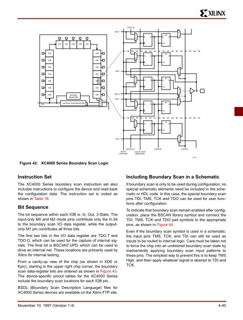
DATA INIOB.T10DQsdD Q01IOBIOBIOB IOB IOBLEIOBIOBIOBIOB10DQsdD QLEIOBIOBIOBIOBIOB.I10IOBIOB10DQsdD QIOBIOBLE1TDIIOBBYPASSREGISTERINSTRUCTION REGISTERIOBMUXTDOIOB.QIOB.T10DQsdD Q001LE10DQsdD QLEIOB.I10SHIFT/CAPTUREDATAOUT UPDATE EXTESTCLOCK DATAREGISTERX9016Figure 42: XC<strong>4000</strong> Series Boundary Scan LogicInstruction SetThe XC<strong>4000</strong> Series boundary scan instruction set alsoincludes instructions to configure the device and read backthe configuration data. The instruction set is coded asshown in Table 18.Bit SequenceThe bit sequence within each IOB is: In, Out, 3-State. Theinput-only M0 and M2 mode pins contribute only the In bitto the boundary scan I/O data register, while the outputonlyM1 pin contributes all three bits.The first two bits in the I/O data register are TDO.T andTDO.O, which can be used for the capture of internal signals.The final bit is BSCANT.UPD, which can be used todrive an internal net. These locations are primarily used by<strong>Xilinx</strong> for internal testing.From a cavity-up view of the chip (as shown in XDE orEpic), starting in the upper right chip corner, the boundaryscan data-register bits are ordered as shown in Figure 43.The device-specific pinout tables for the XC<strong>4000</strong> Seriesinclude the boundary scan locations for each IOB pin.BSDL (Boundary Scan Description Language) files forXC<strong>4000</strong> Series devices are available on the <strong>Xilinx</strong> FTP site.Including Boundary Scan in a SchematicIf boundary scan is only to be used during configuration, nospecial schematic elements need be included in the schematicor HDL code. In this case, the special boundary scanpins TDI, TMS, TCK and TDO can be used for user functionsafter configuration.To indicate that boundary scan remain enabled after configuration,place the BSCAN library symbol and connect theTDI, TMS, TCK and TDO pad symbols to the appropriatepins, as shown in Figure 44.Even if the boundary scan symbol is used in a schematic,the input pins TMS, TCK, and TDI can still be used asinputs to be routed to internal logic. Care must be taken notto force the chip into an undesired boundary scan state byinadvertently applying boundary scan input patterns tothese pins. The simplest way to prevent this is to keep TMSHigh, and then apply whatever signal is desired to TDI andTCK.November 10, 1997 (Version 1.4) 4-45