XC<strong>4000</strong>E and XC<strong>4000</strong>X Series Field Programmable Gate ArraysAdditional Input Latch for Fast Capture (XC<strong>4000</strong>X only)The XC<strong>4000</strong>X IOB has an additional optional latch on theinput. This latch, as shown in Figure 17, is clocked by theoutput clock — the clock used for the output flip-flop —rather than the input clock. Therefore, two different clockscan be used to clock the two input storage elements. Thisadditional latch allows the very fast capture of input data,which is then synchronized to the internal clock by the IOBflip-flop or latch.To use this Fast Capture technique, drive the output clockpin (the Fast Capture latching signal) from the output of oneof the Global Early buffers supplied in the XC<strong>4000</strong>X. Thesecond storage element should be clocked by a GlobalLow-Skew buffer, to synchronize the incoming data to theinternal logic. (See Figure 18.) These special buffers aredescribed in “Global Nets and Buffers (XC<strong>4000</strong>X only)” onpage 4-38.The Fast Capture latch (FCL) is designed primarily for usewith a Global Early buffer. For Fast Capture, a single clocksignal is routed through both a Global Early buffer and aGlobal Low-Skew buffer. (The two buffers share an inputpad.) The Fast Capture latch is clocked by the Global Earlybuffer, and the standard IOB flip-flop or latch is clocked bythe Global Low-Skew buffer. This mode is the safest way touse the Fast Capture latch, because the clock buffers onboth storage elements are driven by the same pad. There isno external skew between clock pads to create potentialproblems.To place the Fast Capture latch in a design, use one of thespecial library symbols, ILFFX or ILFLX. ILFFX is a transparent-LowFast Capture latch followed by an active-Highinput flip-flop. ILFLX is a transparent-Low Fast Capturelatch followed by a transparent-High input latch. Any of theclock inputs can be inverted before driving the library element,and the inverter is absorbed into the IOB. If a singleBUFG output is used to drive both clock inputs, the softwareautomatically runs the clock through both a GlobalLow-Skew buffer and a Global Early buffer, and clocks theFast Capture latch appropriately.Figure 17 on page 4-22 also shows a two-tap delay on theinput. By default, if the Fast Capture latch is used, the <strong>Xilinx</strong>software assumes a Global Early buffer is driving the clock,and selects MEDDELAY to ensure a zero hold time. SelectIPADIPADBUFGEBUFGLSDGFCECILFFXFigure 18: Examples Using XC<strong>4000</strong>X FCLQto internallogicX9013the desired delay based on the discussion in the previoussubsection.IOB Output SignalsOutput signals can be optionally inverted within the IOB,and can pass directly to the pad or be stored in an edgetriggeredflip-flop. The functionality of this flip-flop is shownin Table 12.An active-High 3-state signal can be used to place the outputbuffer in a high-impedance state, implementing 3-stateoutputs or bidirectional I/O. Under configuration control, theoutput (OUT) and output 3-state (T) signals can beinverted. The polarity of these signals is independently configuredfor each IOB.The 4-mA maximum output current specification of many<strong>FPGAs</strong> often forces the user to add external buffers, whichare especially cumbersome on bidirectional I/O lines. TheXC<strong>4000</strong>E and XC<strong>4000</strong>EX/XL devices solve many of theseproblems by providing a guaranteed output sink current of12 mA. Two adjacent outputs can be interconnected externallyto sink up to 24 mA. The XC<strong>4000</strong>E and XC<strong>4000</strong>EX/XL<strong>FPGAs</strong> can thus directly drive buses on a printed circuitboard.By default, the output pull-up structure is configured as aTTL-like totem-pole. The High driver is an n-channel pull-uptransistor, pulling to a voltage one transistor thresholdbelow Vcc. Alternatively, the outputs can be globally configuredas CMOS drivers, with p-channel pull-up transistorspulling to Vcc. This option, applied using the bitstream generationsoftware, applies to all outputs on the device. It isnot individually programmable. In the XC<strong>4000</strong>XL, all outputsare pulled to the positive supply rail.Table 12: Output Flip-Flop Functionality (active risingedge is shown)ModePower-Upor GSRFlip-FlopLegend:X__/SR0*1*ZClockClock Enable T D QX X 0* X SRX 0 0* X Q__/ 1* 0* D DX X 1 X Z0 X 0* X QDon’t careRising edgeSet or Reset value. Reset is default.Input is Low or unconnected (default value)Input is High or unconnected (default value)3-state4-24 November 10, 1997 (Version 1.4)
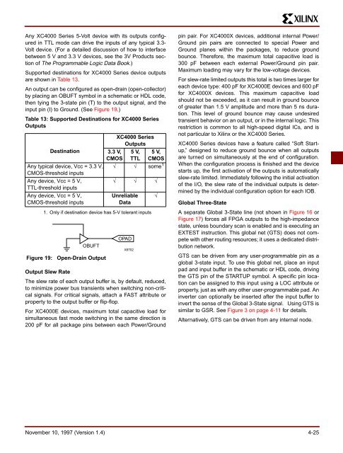
Any XC<strong>4000</strong> Series 5-Volt device with its outputs configuredin TTL mode can drive the inputs of any typical 3.3-Volt device. (For a detailed discussion of how to interfacebetween 5 V and 3.3 V devices, see the 3V Products sectionof The Programmable Logic Data Book.)Supported destinations for XC<strong>4000</strong> Series device outputsare shown in Table 13.An output can be configured as open-drain (open-collector)by placing an OBUFT symbol in a schematic or HDL code,then tying the 3-state pin (T) to the output signal, and theinput pin (I) to Ground. (See Figure 19.)Table 13: Supported Destinations for XC<strong>4000</strong> SeriesOutputsDestinationAny typical device, Vcc = 3.3 V,CMOS-threshold inputsAny device, Vcc = 5 V,TTL-threshold inputsAny device, Vcc = 5 V,CMOS-threshold inputsXC<strong>4000</strong> SeriesOutputs3.3 V,CMOS5 V,TTL5 V,CMOS√ √ some 11. Only if destination device has 5-V tolerant inputsOBUFTFigure 19: Open-Drain Output√ √ √UnreliableDataOPADX6702Output Slew RateThe slew rate of each output buffer is, by default, reduced,to minimize power bus transients when switching non-criticalsignals. For critical signals, attach a FAST attribute orproperty to the output buffer or flip-flop.For XC<strong>4000</strong>E devices, maximum total capacitive load forsimultaneous fast mode switching in the same direction is200 pF for all package pins between each Power/Ground√pin pair. For XC<strong>4000</strong>X devices, additional internal Power/Ground pin pairs are connected to special Power andGround planes within the packages, to reduce groundbounce. Therefore, the maximum total capacitive load is300 pF between each external Power/Ground pin pair.Maximum loading may vary for the low-voltage devices.For slew-rate limited outputs this total is two times larger foreach device type: 400 pF for XC<strong>4000</strong>E devices and 600 pFfor XC<strong>4000</strong>X devices. This maximum capacitive loadshould not be exceeded, as it can result in ground bounceof greater than 1.5 V amplitude and more than 5 ns duration.This level of ground bounce may cause undesiredtransient behavior on an output, or in the internal logic. Thisrestriction is common to all high-speed digital ICs, and isnot particular to <strong>Xilinx</strong> or the XC<strong>4000</strong> Series.XC<strong>4000</strong> Series devices have a feature called “Soft Startup,”designed to reduce ground bounce when all outputsare turned on simultaneously at the end of configuration.When the configuration process is finished and the devicestarts up, the first activation of the outputs is automaticallyslew-rate limited. Immediately following the initial activationof the I/O, the slew rate of the individual outputs is determinedby the individual configuration option for each IOB.Global Three-StateA separate Global 3-State line (not shown in Figure 16 orFigure 17) forces all FPGA outputs to the high-impedancestate, unless boundary scan is enabled and is executing anEXTEST instruction. This global net (GTS) does not competewith other routing resources; it uses a dedicated distributionnetwork.GTS can be driven from any user-programmable pin as aglobal 3-state input. To use this global net, place an inputpad and input buffer in the schematic or HDL code, drivingthe GTS pin of the STARTUP symbol. A specific pin locationcan be assigned to this input using a LOC attribute orproperty, just as with any other user-programmable pad. Aninverter can optionally be inserted after the input buffer toinvert the sense of the Global 3-State signal. Using GTS issimilar to GSR. See Figure 3 on page 4-11 for details.Alternatively, GTS can be driven from any internal node.November 10, 1997 (Version 1.4) 4-25