Xilinx 4000-series FPGAs
Xilinx 4000-series FPGAs
Xilinx 4000-series FPGAs

You also want an ePaper? Increase the reach of your titles
YUMPU automatically turns print PDFs into web optimized ePapers that Google loves.
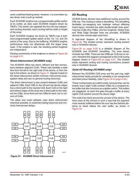
vents undefined floating levels. However, it is overridden byany driver, even a pull-up resistor.Each XC<strong>4000</strong>E longline has a programmable splitter switchat its center, as does each XC<strong>4000</strong>X longline driven byTBUFs. This switch can separate the line into two independentrouting channels, each running half the width or heightof the array.Each XC<strong>4000</strong>X longline not driven by TBUFs has a bufferedprogrammable splitter switch at the 1/4, 1/2, and 3/4points of the array. Due to the buffering, XC<strong>4000</strong>X longlineperformance does not deteriorate with the larger arraysizes. If the longline is split, the resulting partial longlinesare independent.Routing connectivity of the longlines is shown in Figure 28on page 4-31.Direct Interconnect (XC<strong>4000</strong>X only)The XC<strong>4000</strong>X offers two direct, efficient and fast connectionsbetween adjacent CLBs. These nets facilitate a dataflow from the left to the right side of the device, or from thetop to the bottom, as shown in Figure 31. Signals routed onthe direct interconnect exhibit minimum interconnect propagationdelay and use no general routing resources.The direct interconnect is also present between CLBs andadjacent IOBs. Each IOB on the left and top device edgeshas a direct path to the nearest CLB. Each CLB on the rightand bottom edges of the array has a direct path to the nearesttwo IOBs, since there are two IOBs for each row or columnof CLBs.The place and route software uses direct interconnectwhenever possible, to maximize routing resources and minimizeinterconnect delays.I/O RoutingXC<strong>4000</strong> Series devices have additional routing around theIOB ring. This routing is called a VersaRing. The VersaRingfacilitates pin-swapping and redesign without affectingboard layout. Included are eight double-length lines spanningtwo CLBs (four IOBs), and four longlines. Global linesand Wide Edge Decoder lines are provided. XC<strong>4000</strong>Xdevices also include eight octal lines.A high-level diagram of the VersaRing is shown inFigure 32. The shaded arrows represent routing presentonly in XC<strong>4000</strong>X devices.Figure 34 on page 4-35 is a detailed diagram of theXC<strong>4000</strong>E and XC<strong>4000</strong>X VersaRing. The area shownincludes two IOBs. There are two IOBs per CLB row or column,therefore this diagram corresponds to the CLB routingdiagram shown in Figure 28 on page 4-31. The shadedareas represent routing and routing connections presentonly in XC<strong>4000</strong>X devices.Octal I/O Routing (XC<strong>4000</strong>X only)Between the XC<strong>4000</strong>X CLB array and the pad ring, eightinterconnect tracks provide for versatility in pin assignmentand fixed pinout flexibility. (See Figure 33 on page 4-34.)These routing tracks are called octals, because they can bebroken every eight CLBs (sixteen IOBs) by a programmablebuffer that also functions as a splitter switch. The buffersare staggered, so each line goes through a buffer at everyeighth CLB location around the device edge.The octal lines bend around the corners of the device. Thelines cross at the corners in such a way that the segmentmost recently buffered before the turn has the farthest distanceto travel before the next buffer, as shown inFigure 33.IOBIOBIOBIOBIOBIOBIOBIOBIOBIOBCLB~ ~CLB~ ~ ~ ~CLB~ ~CLBCLB~ ~CLBIOBIOBIOBIOBIOBIOBIOBIOBIOBIOBX6603Figure 31: XC<strong>4000</strong>X Direct InterconnectNovember 10, 1997 (Version 1.4) 4-33