Xilinx 4000-series FPGAs
Xilinx 4000-series FPGAs
Xilinx 4000-series FPGAs

You also want an ePaper? Increase the reach of your titles
YUMPU automatically turns print PDFs into web optimized ePapers that Google loves.
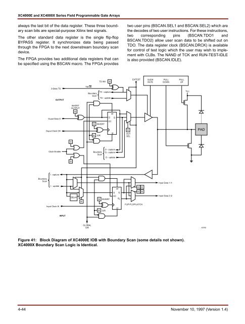
XC<strong>4000</strong>E and XC<strong>4000</strong>X Series Field Programmable Gate Arraysalways the last bit of the data register. These three boundaryscan bits are special-purpose <strong>Xilinx</strong> test signals.The other standard data register is the single flip-flopBYPASS register. It synchronizes data being passedthrough the FPGA to the next downstream boundary scandevice.The FPGA provides two additional data registers that canbe specified using the BSCAN macro. The FPGA providestwo user pins (BSCAN.SEL1 and BSCAN.SEL2) which arethe decodes of two user instructions. For these instructions,two corresponding pins (BSCAN.TDO1 andBSCAN.TDO2) allow user scan data to be shifted out onTDO. The data register clock (BSCAN.DRCK) is availablefor control of test logic which the user may wish to implementwith CLBs. The NAND of TCK and RUN-TEST-IDLEis also provided (BSCAN.IDLE).TS INVMEXTESTSLEWRATEPULLDOWNPULLUP3-State TSOUTPUTTS/OEBoundaryScanTS - captureTS - updateV CCINVERTOUTPUTMsdOuput Data OMINVERTDECQOuput Clock OKMS/RrdMOUTSELPADMClock EnableMBoundaryScanO - captureQ - captureO - updateI - captureBoundaryScanI - updateInput Clock IKDELAYMMMINVERTS/RsdD QECQ LrdM MM MFLIP-FLOP/LATCHInput Data 1 I1Input Data 2 I2INPUTGLOBALS/RX5792Figure 41: Block Diagram of XC<strong>4000</strong>E IOB with Boundary Scan (some details not shown).XC<strong>4000</strong>X Boundary Scan Logic is Identical.4-44 November 10, 1997 (Version 1.4)