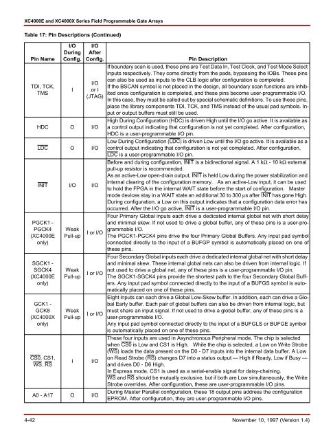
XC<strong>4000</strong>E and XC<strong>4000</strong>X Series Field Programmable Gate ArraysTable 17: Pin Descriptions (Continued)Pin NameTDI, TCK,TMSII/Oor I(JTAG)HDC O I/OLDC O I/OINIT I/O I/OPGCK1 -PGCK4(XC<strong>4000</strong>Eonly)SGCK1 -SGCK4(XC<strong>4000</strong>Eonly)GCK1 -GCK8(XC<strong>4000</strong>Xonly)CS0, CS1,WS, RSI/ODuringConfig.WeakPull-upWeakPull-upWeakPull-upII/OAfterConfig.I or I/OI or I/OI or I/OI/OA0 - A17 O I/OPin DescriptionIf boundary scan is used, these pins are Test Data In, Test Clock, and Test Mode Selectinputs respectively. They come directly from the pads, bypassing the IOBs. These pinscan also be used as inputs to the CLB logic after configuration is completed.If the BSCAN symbol is not placed in the design, all boundary scan functions are inhibitedonce configuration is completed, and these pins become user-programmable I/O.In this case, they must be called out by special schematic definitions. To use these pins,place the library components TDI, TCK, and TMS instead of the usual pad symbols. Inputor output buffers must still be used.High During Configuration (HDC) is driven High until the I/O go active. It is available asa control output indicating that configuration is not yet completed. After configuration,HDC is a user-programmable I/O pin.Low During Configuration (LDC) is driven Low until the I/O go active. It is available as acontrol output indicating that configuration is not yet completed. After configuration,LDC is a user-programmable I/O pin.Before and during configuration, INIT is a bidirectional signal. A 1 kΩ - 10 kΩ externalpull-up resistor is recommended.As an active-Low open-drain output, INIT is held Low during the power stabilization andinternal clearing of the configuration memory. As an active-Low input, it can be usedto hold the FPGA in the internal WAIT state before the start of configuration. Mastermode devices stay in a WAIT state an additional 30 to 300 µs after INIT has gone High.During configuration, a Low on this output indicates that a configuration data error hasoccurred. After the I/O go active, INIT is a user-programmable I/O pin.Four Primary Global inputs each drive a dedicated internal global net with short delayand minimal skew. If not used to drive a global buffer, any of these pins is a user-programmableI/O.The PGCK1-PGCK4 pins drive the four Primary Global Buffers. Any input pad symbolconnected directly to the input of a BUFGP symbol is automatically placed on one ofthese pins.Four Secondary Global inputs each drive a dedicated internal global net with short delayand minimal skew. These internal global nets can also be driven from internal logic. Ifnot used to drive a global net, any of these pins is a user-programmable I/O pin.The SGCK1-SGCK4 pins provide the shortest path to the four Secondary Global Buffers.Any input pad symbol connected directly to the input of a BUFGS symbol is automaticallyplaced on one of these pins.Eight inputs can each drive a Global Low-Skew buffer. In addition, each can drive a GlobalEarly buffer. Each pair of global buffers can also be driven from internal logic, butmust share an input signal. If not used to drive a global buffer, any of these pins is auser-programmable I/O.Any input pad symbol connected directly to the input of a BUFGLS or BUFGE symbolis automatically placed on one of these pins.These four inputs are used in Asynchronous Peripheral mode. The chip is selectedwhen CS0 is Low and CS1 is High. While the chip is selected, a Low on Write Strobe(WS) loads the data present on the D0 - D7 inputs into the internal data buffer. A Lowon Read Strobe (RS) changes D7 into a status output — High if Ready, Low if Busy —and drives D0 - D6 High.In Express mode, CS1 is used as a serial-enable signal for daisy-chaining.WS and RS should be mutually exclusive, but if both are Low simultaneously, the WriteStrobe overrides. After configuration, these are user-programmable I/O pins.During Master Parallel configuration, these 18 output pins address the configurationEPROM. After configuration, they are user-programmable I/O pins.4-42 November 10, 1997 (Version 1.4)
Table 17: Pin Descriptions (Continued)Pin NameA18 - A21(XC<strong>4000</strong>Xonly)OD0 - D7 I I/ODIN I I/ODOUT O I/OUnrestricted User-Programmable I/O PinsI/OI/ODuringConfig.WeakPull-upI/OAfterConfig.Pin DescriptionDuring Master Parallel configuration with an XC<strong>4000</strong>X master, these 4 output pins addI/O 4 more bits to address the configuration EPROM. After configuration, they are user-programmableI/O pins. (See Master Parallel Configuration section for additional details.)During Master Parallel and Peripheral configuration, these eight input pins receive configurationdata. After configuration, they are user-programmable I/O pins.During Slave Serial or Master Serial configuration, DIN is the serial configuration datainput receiving data on the rising edge of CCLK. During Parallel configuration, DIN isthe D0 input. After configuration, DIN is a user-programmable I/O pin.During configuration in any mode but Express mode, DOUT is the serial configurationdata output that can drive the DIN of daisy-chained slave <strong>FPGAs</strong>. DOUT data changeson the falling edge of CCLK, one-and-a-half CCLK periods after it was received at theDIN input.In Express mode, DOUT is the status output that can drive the CS1 of daisy-chained<strong>FPGAs</strong>, to enable and disable downstream devices.After configuration, DOUT is a user-programmable I/O pin.I/OThese pins can be configured to be input and/or output after configuration is completed.Before configuration is completed, these pins have an internal high-value pull-up resistor(25 kΩ - 100 kΩ) that defines the logic level as High.Boundary ScanThe ‘bed of nails’ has been the traditional method of testingelectronic assemblies. This approach has become lessappropriate, due to closer pin spacing and more sophisticatedassembly methods like surface-mount technologyand multi-layer boards. The IEEE Boundary Scan Standard1149.1 was developed to facilitate board-level testing ofelectronic assemblies. Design and test engineers canimbed a standard test logic structure in their device toachieve high fault coverage for I/O and internal logic. Thisstructure is easily implemented with a four-pin interface onany boundary scan-compatible IC. IEEE 1149.1-compatibledevices may be serial daisy-chained together, connectedin parallel, or a combination of the two.The XC<strong>4000</strong> Series implements IEEE 1149.1-compatibleBYPASS, PRELOAD/SAMPLE and EXTEST boundaryscan instructions. When the boundary scan configurationoption is selected, three normal user I/O pins become dedicatedinputs for these functions. Another user output pinbecomes the dedicated boundary scan output. The detailsof how to enable this circuitry are covered later in this section.By exercising these input signals, the user can serially loadcommands and data into these devices to control the drivingof their outputs and to examine their inputs. Thismethod is an improvement over bed-of-nails testing. Itavoids the need to over-drive device outputs, and it reducesthe user interface to four pins. An optional fifth pin, a resetfor the control logic, is described in the standard but is notimplemented in <strong>Xilinx</strong> devices.The dedicated on-chip logic implementing the IEEE 1149.1functions includes a 16-state machine, an instruction registerand a number of data registers. The functional detailscan be found in the IEEE 1149.1 specification and are alsodiscussed in the <strong>Xilinx</strong> application note XAPP 017: “BoundaryScan in XC<strong>4000</strong> Devices.”Figure 41 on page 4-44 shows a simplified block diagram ofthe XC<strong>4000</strong>E Input/Output Block with boundary scanimplemented. XC<strong>4000</strong>X boundary scan logic is identical.Figure 42 on page 4-45 is a diagram of the XC<strong>4000</strong> Seriesboundary scan logic. It includes three bits of Data Registerper IOB, the IEEE 1149.1 Test Access Port controller, andthe Instruction Register with decodes.XC<strong>4000</strong> Series devices can also be configured through theboundary scan logic. See “Readback” on page 4-56.Data RegistersThe primary data register is the boundary scan register. Foreach IOB pin in the FPGA, bonded or not, it includes threebits for In, Out and 3-State Control. Non-IOB pins haveappropriate partial bit population for In or Out only. PRO-GRAM, CCLK and DONE are not included in the boundaryscan register. Each EXTEST CAPTURE-DR state capturesall In, Out, and 3-state pins.The data register also includes the following non-pin bits:TDO.T, and TDO.O, which are always bits 0 and 1 of thedata register, respectively, and BSCANT.UPD, which isNovember 10, 1997 (Version 1.4) 4-43