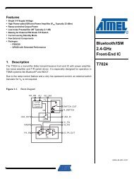
JANSR2N7389 JANSF2N7389 HEXFET® TRANSISTOR IRHF9130 ...
JANSR2N7389 JANSF2N7389 HEXFET® TRANSISTOR IRHF9130 ...
JANSR2N7389 JANSF2N7389 HEXFET® TRANSISTOR IRHF9130 ...

Create successful ePaper yourself
Turn your PDF publications into a flip-book with our unique Google optimized e-Paper software.
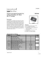
REVIEW ONLY<strong>IRHF9130</strong>, IRHF93130, JANSR-, JANSF-, 2N7389 DevicePre-IrradiationElectrical Characteristics @ Tj = 25°C (Unless Otherwise Specified)Parameter Min Typ Max Units Test ConditionsBVDSS Drain-to-Source Breakdown Voltage -100 — — V VGS =0 V, ID = -1.0mADBVDSS/DTJ Temperature Coefficient of Breakdown — -0.112 — V/°C Reference to 25°C, ID = -1.0mAVoltageRDS(on) Static Drain-to-Source — — 0.30 VGS = -12V, ID = -4.1A „On-State Resistance — — 0.35 W VGS = -12V, ID = -6.5AVGS(th) Gate Threshold Voltage -2.0 — -4.0 V VDS = VGS, ID = -1.0mAgfs Forward Transconductance 2.5 — — S ( ) VDS > -15V, IDS = -4.1A „IDSS Zero Gate Voltage Drain Current — — -25 VDS= 0.8 x Max Rating,VGS=0VmA— — -250 VDS = 0.8 x Max RatingVGS = 0V, TJ = 125°CIGSS Gate-to-Source Leakage Forward — — -100 VGS = -20VnAIGSS Gate-to-Source Leakage Reverse — — 100 VGS = 20VQg Total Gate Charge — — 45 VGS = -12V, ID = -6.5AQgs Gate-to-Source Charge — — 10 nC VDS = Max Rating x 0.5Qgd Gate-to-Drain (‘Miller’) Charge — — 25td(on) Turn-On Delay Time — — 30 VDD = -50V, ID = -6.5A,tr Rise Time — — 50 RG = 7.5Wnstd(off) Turn-Off Delay Time — — 70tf Fall Time — — 70LD Internal Drain Inductance — 5.0 —LS Internal Source Inductance — 13 —nHWMeasured from drain lead,6mm (0.25 in) from packageto center of die.Measured from source lead,6mm (0.25 in) from packageto source bonding pad.Modified MOSFET symbol showingthe internal inductances.Ciss Input Capacitance — 1200 — VGS = 0V, VDS = -25VCoss Output Capacitance — 290 — pF f = 1.0MHzCrss Reverse Transfer Capacitance — 76 —Source-Drain Diode Ratings and CharacteristicsParameter Min Typ Max Units Test ConditionsIS Continuous Source Current (Body Diode) — — -6.5 Modified MOSFET symbol showing the integralAISM Pulse Source Current (Body Diode) — — -26 reverse p-n junction rectifier.VSD Diode Forward Voltage — — -3.0 V Tj = 25°C, IS = -6.5A, VGS = 0V „trr Reverse Recovery Time — — 250 ns Tj = 25°C, IF = -6.5A, di/dt £ -100A/msQRR Reverse Recovery Charge — — 0.74 mC VDD £ -50V „ton Forward Turn-On Time Intrinsic turn-on time is negligible. Turn-on speed is substantially controlled by LS + LD.Thermal ResistanceParameter Min Typ Max Units Test ConditionsRthJC Junction-to-Case — — 5.0°C/WRthJA Junction-to-Ambient — 175 — Typical socket mount2 www.irf.com