JANSR2N7389 JANSF2N7389 HEXFET® TRANSISTOR IRHF9130 ...
JANSR2N7389 JANSF2N7389 HEXFET® TRANSISTOR IRHF9130 ...
JANSR2N7389 JANSF2N7389 HEXFET® TRANSISTOR IRHF9130 ...

You also want an ePaper? Increase the reach of your titles
YUMPU automatically turns print PDFs into web optimized ePapers that Google loves.
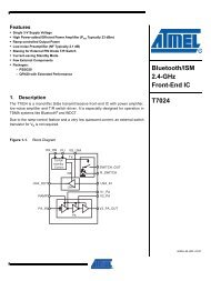
REVIEW ONLY<strong>IRHF9130</strong>, IRHF93130, JANSR-, JANSF-, 2N7389 DevicePre-Irradiation7.0V DSR D-I D , Drain Current (A)6.05.04.03.02.01.00.025 50 75 100 125 150T C , Case Temperature ( ° C)Fig 9. Maximum Drain Current Vs.Case TemperatureR GV GS-12VPulse Width £1 µsDuty Factor £ 0.1 %D.U.T.Fig 10a. Switching Time Test CircuitV GSt d(on) t r t d(off) t f10%90%V DSFig 10b. Switching Time Waveforms+-V DD10Thermal Response (Z thJC )10.10.500.200.100.050.020.01SINGLE PULSE(THERMAL RESPONSE)Notes:1. Duty factor D = t 1 / t 22. Peak T J = P DM x Z thJC + TC0.010.00001 0.0001 0.001 0.01 0.1 1 10t 1, Rectangular Pulse Duration (sec)PDMt1t2Fig 11. Maximum Effective Transient Thermal Impedance, Junction-to-Case6 www.irf.com