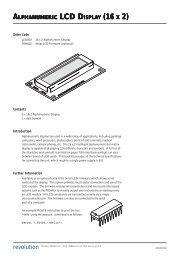
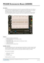
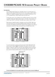
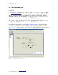
You also want an ePaper? Increase the reach of your titles
YUMPU automatically turns print PDFs into web optimized ePapers that Google loves.
LD1117A SERIESELECTRICAL CHARACTERISTICS OF LD1117A#18 (refer to the test circuits, T J = 0 to 125°C,C O =10µF,C I = 10 µF unless otherwise specified)60 80 dBSymbol Parameter Test Conditions Min. Typ. Max. UnitV O Output Voltage V I = 3.8 V I O =10mA T J = 25°C 1.764 1.8 1.836 VV O Output Voltage I O =0to1A V I = 3.3 to 8 V 1.728 1.872 V∆V O Line Regulation V I = 3.3 to 8 V I O = 0 mA 1 6 mV∆V O Load Regulation V I = 3.3 V I O = 0 to 1 A 1 10 mV∆V O Temperature Stability 0.5 %∆V O Long Term Stability 1000 hrs, T J = 125°C 0.3 %V I Operating Input Voltage I O = 100 mA 10 VI d Quiescent Current V I ≤ 8V I O = 0 mA 5 10 mAI O Output Current V I -V O =5VT J = 25°C 1000 mAeN Output Noise Voltage B =10Hz to 10KHz T J = 25°C 100 µVSVR Supply Voltage Rejection I O = 40 mA f = 120HzV I -V O =3V V ripple =1V PPV D Dropout Voltage I O = 100 mA 1 1.10 VI O = 500 mA 1.05 1.15I O = 1 A 1.15 1.30∆V O(pwr) Thermal Regulation T a = 25°C 30ms Pulse 0.08 0.2 %/WELECTRICAL CHARACTERISTICS OF LD1117A#25 (refer to the test circuits, T J = 0 to 125°C,C O =10µF,C I = 10 µF unless otherwise specified)60 80 dBSymbol Parameter Test Conditions Min. Typ. Max. UnitV O Output Voltage V I = 4.5 V I O =10mA T J = 25°C 2.45 2.5 2.55 VV O Output Voltage I O =0to1A V I = 3.9 to 8 V 2.4 2.6 V∆V O Line Regulation V I = 3.9 to 8 V I O = 0 mA 1 6 mV∆V O Load Regulation V I = 3.9 V I O = 0 to 1 A 1 10 mV∆V O Temperature Stability 0.5 %∆V O Long Term Stability 1000 hrs, T J = 125°C 0.3 %V I Operating Input Voltage I O = 100 mA 10 VI d Quiescent Current V I ≤ 10 V I O = 0 mA 5 10 mAI O Output Current V I -V O =5VT J = 25°C 1000 1200 mAeN Output Noise Voltage B =10Hz to 10KHz T J = 25°C 100 µVSVR Supply Voltage Rejection I O = 40 mA f = 120HzV I -V O =3V V ripple =1V PPV D Dropout Voltage I O = 100 mA 1 1.10 VI O = 500 mA 1.05 1.15I O = 1 A 1.15 1.30∆V O(pwr) Thermal Regulation T a = 25°C 30ms Pulse 0.08 0.2 %/W4/16