Dual 10-Ohm SPDT Analog Switch (Rev. D)
Dual 10-Ohm SPDT Analog Switch (Rev. D)
Dual 10-Ohm SPDT Analog Switch (Rev. D)

You also want an ePaper? Increase the reach of your titles
YUMPU automatically turns print PDFs into web optimized ePapers that Google loves.
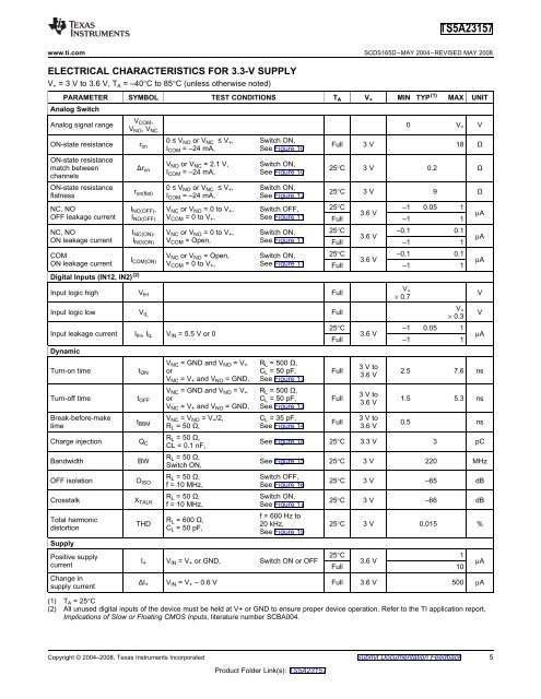
TS5A23157www.ti.com ................................................................................................................................................................ SCDS165D–MAY 2004–REVISED MAY 2008ELECTRICAL CHARACTERISTICS FOR 3.3-V SUPPLYV + = 3 V to 3.6 V, T A = –40°C to 85°C (unless otherwise noted)PARAMETER SYMBOL TEST CONDITIONS T A V + MIN TYP (1) MAX UNIT<strong>Analog</strong> <strong>Switch</strong>V COM ,<strong>Analog</strong> signal range 0 V + VV NO , V NC0 ≤ V NO or V NC ≤ V + , <strong>Switch</strong> ON,ON-state resistance r on Full 3 V 18 ΩI COM = –24 mA, See Figure <strong>10</strong>ON-state resistanceV NO or V NC = 2.1 V, <strong>Switch</strong> ON,match between Δr on 25°C 3 V 0.2 ΩI COM = –24 mA, See Figure <strong>10</strong>channelsON-state resistance 0 ≤ V NO or V NC ≤ V + , <strong>Switch</strong> ON,r on(flat) 25°C 3 V 9 Ωflatness I COM = –24 mA, See Figure 12NC, NO I NC(OFF) , V NC or V NO = 0 to V + , <strong>Switch</strong> OFF, 25°C –1 0.05 13.6 V µAOFF leakage current I NO(OFF) V COM = 0 to V + , See Figure 11 Full –1 1NC, NO I NC(ON) , V NC or V NO = 0 to V + , <strong>Switch</strong> ON, 25°C –0.1 0.13.6 V µAON leakage current I NO(ON) V COM = Open, See Figure 11 Full –1 1COM V NC or V NO = Open, <strong>Switch</strong> ON, 25°C –0.1 0.1I COM(ON) 3.6 V µAON leakage current V COM = 0 to V + , See Figure 11 Full –1 1Digital Inputs (IN12, IN2) (2) V +Input logic high VIH Full V× 0.7V +Input logic low VIL Full V× 0.325°C –1 0.05 1Input leakage current I IH , I IL V IN = 5.5 V or 0 3.6 V µAFull –1 1DynamicV NC = GND and V NO = V + R L = 500 Ω,3 V toTurn-on time t ON or C L = 50 pF, Full 2.5 7.6 ns3.6 VV NC = V + and V NO = GND, See Figure 13V NC = GND and V NO = V + R L = 500 Ω,3 V toTurn-off time t OFF or C L = 50 pF, Full 1.5 5.3 ns3.6 VV NC = V + and V NO = GND, See Figure 13Break-before-make V NC = V NO = V + /2, C L = 35 pF, 3 V tot BBM Full 0.5 nstime R L = 50 Ω, See Figure 14 3.6 VR L = 50 Ω,Charge injection Q C See Figure 18 25°C 3.3 V 3 pCCL = 0.1 nF,R L = 50 Ω,Bandwidth BW See Figure 15 25°C 3 V 220 MHz<strong>Switch</strong> ON,R L = 50 Ω,<strong>Switch</strong> OFF,OFF isolation O ISO 25°C 3 V –65 dBf = <strong>10</strong> MHz, See Figure 16R L = 50 Ω,<strong>Switch</strong> ON,Crosstalk X TALK 25°C 3 V –66 dBf = <strong>10</strong> MHz, See Figure 17f = 600 Hz toTotal harmonic R L = 600 Ω,THD 20 kHz, 25°C 3 V 0.015 %distortionC L = 50 pF,See Figure 19SupplyPositive supply25°C 1I + V IN = V + or GND, <strong>Switch</strong> ON or OFF 3.6 V µAcurrent Full <strong>10</strong>Change insupply currentΔI + V IN = V + – 0.6 V Full 3.6 V 500 µA(1) T A = 25°C(2) All unused digital inputs of the device must be held at V+ or GND to ensure proper device operation. Refer to the TI application report,Implications of Slow or Floating CMOS Inputs, literature number SCBA004.Copyright © 2004–2008, Texas Instruments Incorporated Submit Documentation Feedback 5Product Folder Link(s): TS5A23157