Dual 10-Ohm SPDT Analog Switch (Rev. D)
Dual 10-Ohm SPDT Analog Switch (Rev. D)
Dual 10-Ohm SPDT Analog Switch (Rev. D)

Create successful ePaper yourself
Turn your PDF publications into a flip-book with our unique Google optimized e-Paper software.
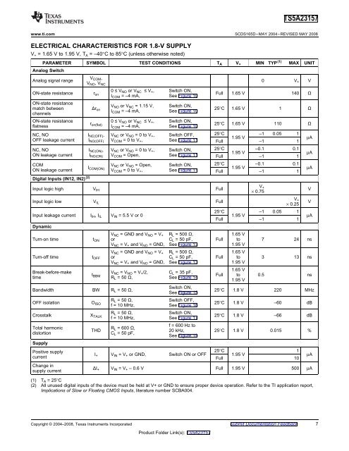
TS5A23157www.ti.com ................................................................................................................................................................ SCDS165D–MAY 2004–REVISED MAY 2008ELECTRICAL CHARACTERISTICS FOR 1.8-V SUPPLYV + = 1.65 V to 1.95 V, T A = –40°C to 85°C (unless otherwise noted)PARAMETER SYMBOL TEST CONDITIONS T A V + MIN TYP (1) MAX UNIT<strong>Analog</strong> <strong>Switch</strong>V COM ,<strong>Analog</strong> signal range 0 V + VV NO , V NC0 ≤ V NO or V NC ≤ V + , <strong>Switch</strong> ON,ON-state resistance r on Full 1.65 V 140 ΩI COM = –4 mA, See Figure <strong>10</strong>ON-state resistanceV NO or V NC = 1.15 V, <strong>Switch</strong> ON,match between Δr on 25°C 1.65 V 1 ΩI COM = –4 mA, See Figure <strong>10</strong>channelsON-state resistance 0 ≤ V NO or V NC ≤ V + , <strong>Switch</strong> ON,r on(flat) 25°C 1.65 V 1<strong>10</strong> Ωflatness I COM = –4 mA, See Figure <strong>10</strong>NC, NO I NC(OFF) , V NC or V NO = 0 to V + , <strong>Switch</strong> OFF, 25°C –1 0.05 11.95 V µAOFF leakage current I NO(OFF) V COM = 0 to V + , See Figure 11 Full –1 1NC, NO I NC(ON) , V NC or V NO = 0 to V + , <strong>Switch</strong> ON, 25°C –0.1 0.11.95 V µAON leakage current I NO(ON) V COM = Open, See Figure 11 Full –1 1COM V NC or V NO = Open, <strong>Switch</strong> ON, 25°C –0.1 0.1I COM(ON) 1.95 V µAON leakage current V COM = 0 to V + , See Figure 11 Full –1 1Digital Inputs (IN12, IN2) (2) V +Input logic high VIH Full V× 0.75V +Input logic low VIL Full V× 0.2525°C –1 0.05 1Input leakage current I IH , I IL V IN = 5.5 V or 0 1.95 V µAFull –1 1DynamicV NC = GND and V NO = V + R L = 500 Ω, 1.65 VTurn-on time t ON or C L = 50 pF, Full to 7 24 nsV NC = V + and V NO = GND, See Figure 13 1.95 VV NC = GND and V NO = V + R L = 500 Ω, 1.65 VTurn-off time t OFF or C L = 50 pF, Full to 3 13 nsV NC = V + and V NO = GND, See Figure 13 1.95 V1.65 VBreak-before-make V NC = V NO = V + /2, C L = 35 pF,t BBM Full to 0.5 nstime R L = 50 Ω, See Figure 141.95 V<strong>Switch</strong> ON,Bandwidth BW R L = 50 Ω, 25°C 1.8 V 220 MHzSee Figure 15R L = 50 Ω,<strong>Switch</strong> OFF,OFF isolation O ISO 25°C 1.8 V –60 dBf = <strong>10</strong> MHz, See Figure 16R L = 50 Ω,<strong>Switch</strong> ON,Crosstalk X TALK 25°C 1.8 V –66 dBf = <strong>10</strong> MHz, See Figure 17f = 600 Hz toTotal harmonic R L = 600 Ω,THD 20 kHz, 25°C 1.8 V 0.015 %distortionC L = 50 pF,See Figure 19SupplyPositive supply25°C 1I + V IN = V + or GND, <strong>Switch</strong> ON or OFF 1.95 V µAcurrent Full <strong>10</strong>Change insupply currentΔI + V IN = V + – 0.6 V Full 1.95 V 500 µA(1) T A = 25°C(2) All unused digital inputs of the device must be held at V+ or GND to ensure proper device operation. Refer to the TI application report,Implications of Slow or Floating CMOS Inputs, literature number SCBA004.Copyright © 2004–2008, Texas Instruments Incorporated Submit Documentation Feedback 7Product Folder Link(s): TS5A23157