
Create successful ePaper yourself
Turn your PDF publications into a flip-book with our unique Google optimized e-Paper software.
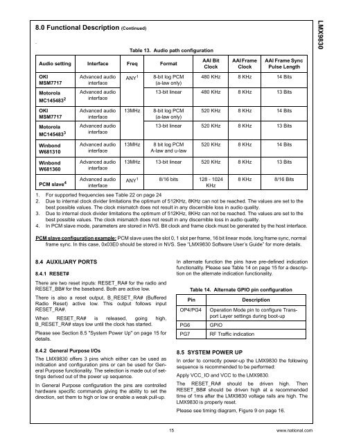
8.0 Functional Description (Continued).Table 13. Audio path configuration<strong>LMX9830</strong>Audio setting Interface Freq FormatAAI BitClockAAI FrameClockAAI Frame SyncPulse LengthOKIMSM7717Advanced audiointerfaceANY 18-bit log PCM(a-law only)480 KHz 8 KHz 14 BitsMotorolaMC145483 2Advanced audiointerface13-bit linear 480 KHz 8 KHz 13 BitsOKIMSM7717Advanced audiointerface13MHz8-bit log PCM(a-law only)520 KHz 8 KHz 14 BitsMotorolaMC145483 3Advanced audiointerface13-bit linear 520 KHz 8 KHz 13 BitsWinbondW681310Advanced audiointerface13MHz8 bit log PCMA-law and u-law520 KHz 8 KHz 14 BitsWinbondW681360Advanced audiointerface13MHz 13-bit linear 520 KHz 8 KHz 13 BitsPCM slave 4Advanced audiointerfaceANY 1 8/16 bits 128 - 1024KHz8 KHz 8/16 Bits1. For supported frequencies see Table 22 on page 242. Due to internal clock divider limitations the optimum of 512KHz, 8KHz can not be reached. The values are set to thebest possible values. The clock mismatch does not result in any discernible loss in audio quality.3. Due to internal clock divider limitations the optimum of 512KHz, 8KHz can not be reached. The values are set to thebest possible values. The clock mismatch does not result in any discernible loss in audio quality.4. In PCM slave mode, parameters are stored in NVS. Bit clock and frame clock must be generated by the host interface.PCM slave configuration example: PCM slave uses the slot 0, 1 slot per frame, 16 bit linear mode, long frame sync, normalframe sync. In this case, 0x03E0 should be stored in NVS. See “<strong>LMX9830</strong> Software User’s Guide” for more details.8.4 AUXILIARY PORTS8.4.1 RESET#There are two reset inputs: RESET_RA# for the radio andRESET_BB# for the baseband. Both are active low.There is also a reset output, B_RESET_RA# (BufferedRadio Reset) active low. This output follows inputRESET_RA#.When RESET_RA# is released, going high,B_RESET_RA# stays low until the clock has started.Please see Section 8.5 "System Power Up" on page 15 fordetails.8.4.2 General Purpose I/OsThe <strong>LMX9830</strong> offers 3 pins which either can be used asindication and configuration pins or can be used for GeneralPurpose functionality. The selection is made out of settingsderived out of the power up sequence.In General Purpose configuration the pins are controlledhardware specific commands giving the ability to set thedirection, set them to high or low or enable a weak pull-up.In alternate function the pins have pre-defined indicationfunctionality. Please see Table 14 on page 15 for a descriptionon the alternate indication functionality.Table 14. Alternate GPIO pin configurationPinOP4/PG4PG6PG7DescriptionOperation Mode pin to configure TransportLayer settings during boot-upGPIORF Traffic indication8.5 SYSTEM POWER UPIn order to correctly power-up the <strong>LMX9830</strong> the followingsequence is recommended to be performed:Apply VCC_IO and VCC to the <strong>LMX9830</strong>.The RESET_RA# should be driven high. ThenRESET_BB# should be driven high at a recommendedtime of 1ms after the <strong>LMX9830</strong> voltage rails are high. The<strong>LMX9830</strong> is properly reset.Please see timing diagram, Figure 9 on page 16.15 www.national.com