
Create successful ePaper yourself
Turn your PDF publications into a flip-book with our unique Google optimized e-Paper software.
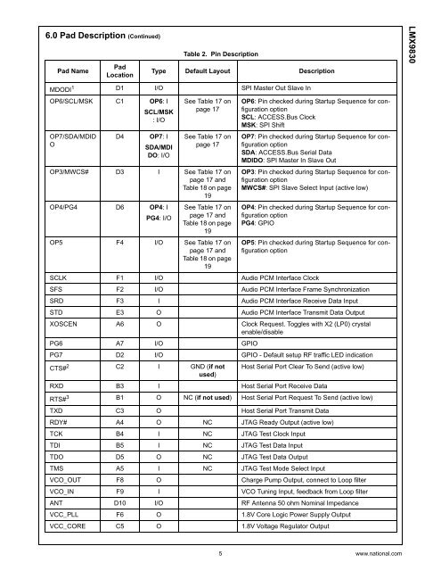
6.0 Pad Description (Continued)Pad NamePadLocationTable 2. Pin DescriptionType Default Layout Description<strong>LMX9830</strong>MDODI 1 D1 I/O SPI Master Out Slave InOP6/SCL/MSK C1 OP6: I See Table 17 onpage 17OP7/SDA/MDIDOD4SCL/MSK: I/OOP7: ISDA/MDIDO: I/OSee Table 17 onpage 17OP3/MWCS# D3 I See Table 17 onpage 17 andTable 18 on page19OP4/PG4 D6 OP4: IPG4: I/OSee Table 17 onpage 17 andTable 18 on page19OP5 F4 I/O See Table 17 onpage 17 andTable 18 on page19OP6: Pin checked during Startup Sequence for configurationoptionSCL: ACCESS.Bus ClockMSK: SPI ShiftOP7: Pin checked during Startup Sequence for configurationoptionSDA: ACCESS.Bus <strong>Serial</strong> DataMDIDO: SPI Master In Slave OutOP3: Pin checked during Startup Sequence for configurationoptionMWCS#: SPI Slave Select Input (active low)OP4: Pin checked during Startup Sequence for configurationoptionPG4: GPIOOP5: Pin checked during Startup Sequence for configurationoptionSCLK F1 I/O Audio PCM Interface ClockSFS F2 I/O Audio PCM Interface Frame SynchronizationSRD F3 I Audio PCM Interface Receive Data InputSTD E3 O Audio PCM Interface Transmit Data OutputXOSCEN A6 O Clock Request. Toggles with X2 (LP0) crystalenable/disablePG6 A7 I/O GPIOPG7 D2 I/O GPIO - Default setup RF traffic LED indicationCTS# 2 C2 I GND (if not Host <strong>Serial</strong> <strong>Port</strong> Clear To Send (active low)used)RXD B3 I Host <strong>Serial</strong> <strong>Port</strong> Receive DataRTS# 3 B1 O NC (if not used) Host <strong>Serial</strong> <strong>Port</strong> Request To Send (active low)TXD C3 O Host <strong>Serial</strong> <strong>Port</strong> Transmit DataRDY# A4 O NC JTAG Ready Output (active low)TCK B4 I NC JTAG Test Clock InputTDI B5 I NC JTAG Test Data InputTDO D5 O NC JTAG Test Data OutputTMS A5 I NC JTAG Test Mode Select InputVCO_OUT F8 O Charge Pump Output, connect to Loop filterVCO_IN F9 I VCO Tuning Input, feedback from Loop filterANT D10 I/O RF Antenna 50 ohm Nominal ImpedanceVCC_PLL F6 O 1.8V Core Logic Power Supply OutputVCC_CORE C5 O 1.8V Voltage Regulator Output5 www.national.com