Protection Design Guide for Portable Electronics - Semtech
Protection Design Guide for Portable Electronics - Semtech
Protection Design Guide for Portable Electronics - Semtech

You also want an ePaper? Increase the reach of your titles
YUMPU automatically turns print PDFs into web optimized ePapers that Google loves.
PROTECTION PRODUCTS<br />
ESD Compliance Standard - IEC 61000-4-2<br />
Several models exist to simulate the ESD event. Each<br />
is designed to describe the threat in a real world<br />
environment. The discharge model is typically a<br />
voltage source feeding a resistor/capacitor network.<br />
Resistor and capacitor values vary depending upon the<br />
standard. Today the most internationally recognized<br />
ESD standard is IEC 61000-4-2. IEC 61000-4-2 is<br />
a system level standard used by manufacturers to<br />
model ESD events from human contact. The test is<br />
per<strong>for</strong>med by discharging a 150pF capacitor through<br />
a 330 ohm resistor. The peak current achieved is<br />
approximately 5 times greater than that of component<br />
level ESD tests such as JEDEC STD 883, Method 3015.<br />
This is one reason why devices may fail at the system<br />
level even though they pass the component level test.<br />
Discharge into the equipment may be through direct<br />
contact (contact discharge) or just prior to contact (air<br />
discharge). IEC 61000-4-2 divides the ESD into four<br />
© 2009 <strong>Semtech</strong> Corp.<br />
Introduction<br />
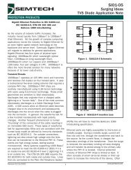
ESD Testing - IEC 61000-4-2<br />
ESD Wave<strong>for</strong>m and Discharge Levels per IEC 61000-4-2<br />
4<br />
SI08-01<br />
<strong>Protection</strong> <strong>Design</strong> <strong>Guide</strong><br />
<strong>for</strong> <strong>Portable</strong> <strong>Electronics</strong><br />
threat levels. Test voltages at the threat levels range<br />
from 2kV to 15kV with peak discharge currents as<br />
high as 30A. Most manufacturers adhere to the most<br />
stringent level, level 4, which defines a +/-15kV air<br />
discharge test and a +/-8kV contact discharge test.<br />
However, many manufacturers test their equipment<br />
beyond these levels. The ESD wave<strong>for</strong>m as defined<br />
by IEC 61000-4-2 reaches peak magnitude in 700ps<br />
to 1ns and has a total duration of only 60ns. While<br />
the ESD pulse contains little energy, the resulting<br />
effect can be devastating to sensitive semiconductor<br />
devices. Sensitive points of the equipment are to be<br />
tested with a combination of positive and negative<br />
discharges. Sensitive areas of a cell phone <strong>for</strong> example<br />
would include I/O ports, audio ports, battery contacts,<br />
LED displays, antenna, external memory ports, and the<br />
keypad.<br />
Level<br />
Test<br />
Voltage<br />
Air Discharge<br />
(kV)<br />
Test<br />
Voltage<br />
Contact<br />
Discharge<br />
(kV)<br />
First<br />
Peak<br />
Current<br />
(A)<br />
Peak<br />
Current<br />
at 30ns<br />
(A)<br />
Peak<br />
Current<br />
at 60ns<br />
(A)<br />
1 2 2 7.5 4 2<br />
2 4 4 15 8 4<br />
3 8 6 22.5 12 6<br />
4 15 8 30 16 8<br />
www.semtech.com