CMOS Production Compatible SiGe Heteroepitaxy for High ... - Imec
CMOS Production Compatible SiGe Heteroepitaxy for High ... - Imec
CMOS Production Compatible SiGe Heteroepitaxy for High ... - Imec

You also want an ePaper? Increase the reach of your titles
YUMPU automatically turns print PDFs into web optimized ePapers that Google loves.
Ge Content (%)<br />
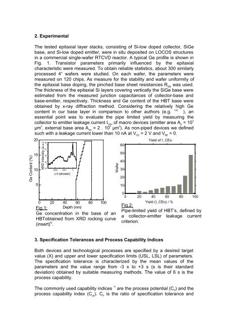
2. Experimental<br />
The tested epitaxial layer stacks, consisting of Si-low doped collector, <strong>SiGe</strong><br />
base, and Si-low doped emitter, were in situ deposited on LOCOS structures<br />
in a commercial single-wafer RTCVD reactor. A typical Ge profile is shown in<br />
Fig. 1. Transistor parameters primarily influenced by the epitaxial<br />
characteristic were measured. To obtain reliable statistics, about 300 similarly<br />
processed 4“ wafers were studied. On each wafer, the parameters were<br />
measured on 120 chips. As measure <strong>for</strong> the stability and wafer uni<strong>for</strong>mity of<br />
the epitaxial base doping, the pinched base sheet resistances R SBi was used.<br />
The thickness of the epitaxial Si layers covering vertically the <strong>SiGe</strong> base were<br />
estimated from the measured junction capacitances of collector-base and<br />
base-emitter, respectively. Thickness and Ge content of the HBT base were<br />
obtained by x-ray diffraction method. Considering the relatively high Ge<br />
content in our base layer in comparison to other authors (e.g. 3,4) ), an<br />
essential point was to evaluate the pipe limited yield by measuring the<br />
collector to emitter leakage current I CE0 of macro devices (emitter area A E = 10 4<br />
µm 2 , external base area A ext = 2 . 10 4 µm 2 ). As non-piped devices we defined<br />
such with a leakage current lower than 10 nA at V CE = 2 V and V BE = 0.<br />
20<br />
15<br />
10<br />
5<br />
XRD Intensity (a.u.)<br />
10<br />
5<br />
-2<br />
10 -2<br />
10<br />
5<br />
-3<br />
10 -3<br />
10<br />
5<br />
-4<br />
10 -4<br />
10<br />
5<br />
-5<br />
10 -5<br />
10 -6<br />
10 -6<br />
-2000 -1000 0<br />
Δ θ (arcsec)<br />
Fig.1:<br />
Ge concentration in the base of an<br />
HBTobtained from XRD rocking curve<br />
(insert) 6) 0 20 40 60 80 100<br />
Depth (nm)<br />
.<br />
Fig.2:<br />
Pipe-limited yield of HBT’s, defined by<br />
a collector-emitter leakage current<br />
criterion.<br />
3. Specification Tolerances and Process Capability Indices<br />
Wafer<br />
0<br />
0 20 40 60 80 100<br />
Both devices and technological processes are specified by a desired target<br />
value (X) and upper and lower specification limits (USL, LSL) of parameters.<br />
The specification tolerance is characterized by the mean values of the<br />
parameters and the value range from -3 s to +3 s (s is their standard<br />
deviation) obtained by suitable measuring methods. The value of 6 s is the<br />
process capability.<br />
The commonly used capability indices 7) are the process potential (C P ) and the<br />
process capability index (C pk ). C P is the ratio of specification tolerance and<br />
60<br />
50<br />
40<br />
30<br />
20<br />
10<br />
Yield of I_CEo<br />
Yield (I_CEo) / %