CMOS Production Compatible SiGe Heteroepitaxy for High ... - Imec
CMOS Production Compatible SiGe Heteroepitaxy for High ... - Imec
CMOS Production Compatible SiGe Heteroepitaxy for High ... - Imec

You also want an ePaper? Increase the reach of your titles
YUMPU automatically turns print PDFs into web optimized ePapers that Google loves.
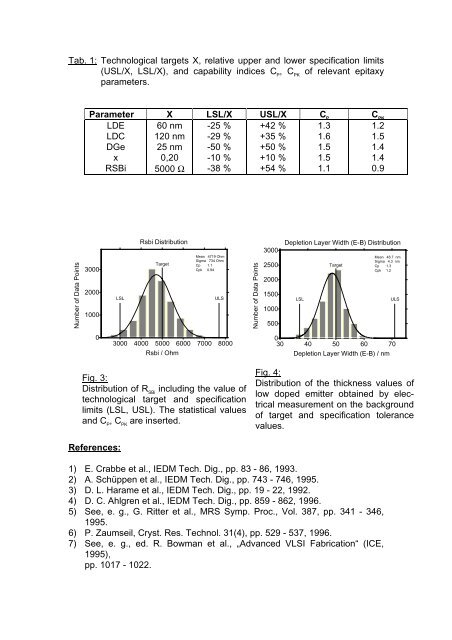
Tab. 1: Technological targets X, relative upper and lower specification limits<br />
(USL/X, LSL/X), and capability indices C P , C PK of relevant epitaxy<br />
parameters.<br />
Number of Data Points<br />
Parameter X LSL/X USL/X C P C PK<br />
3000<br />
2000<br />
1000<br />
0<br />
LDE<br />
LDC<br />
DGe<br />
x<br />
RSBi<br />
References:<br />
60 nm<br />
120 nm<br />
25 nm<br />
0,20<br />
5000 Ω<br />
Rsbi Distribution<br />
Target<br />
-25 %<br />
-29 %<br />
-50 %<br />
-10 %<br />
-38 %<br />
Mean 4719 Ohm<br />
Sigma 734 Ohm<br />
Cp 1.1<br />
Cpk 0.94<br />
LSL ULS<br />
3000 4000 5000 6000 7000 8000<br />
Rsbi / Ohm<br />
Fig. 3:<br />
Distribution of R SBi including the value of<br />
technological target and specification<br />
limits (LSL, USL). The statistical values<br />
and C P , C PK are inserted.<br />
+42 %<br />
+35 %<br />
+50 %<br />
+10 %<br />
+54 %<br />
1) E. Crabbe et al., IEDM Tech. Dig., pp. 83 - 86, 1993.<br />
2) A. Schüppen et al., IEDM Tech. Dig., pp. 743 - 746, 1995.<br />
3) D. L. Harame et al., IEDM Tech. Dig., pp. 19 - 22, 1992.<br />
4) D. C. Ahlgren et al., IEDM Tech. Dig., pp. 859 - 862, 1996.<br />
5) See, e. g., G. Ritter et al., MRS Symp. Proc., Vol. 387, pp. 341 - 346,<br />
1995.<br />
6) P. Zaumseil, Cryst. Res. Technol. 31(4), pp. 529 - 537, 1996.<br />
7) See, e. g., ed. R. Bowman et al., „Advanced VLSI Fabrication“ (ICE,<br />
1995),<br />
pp. 1017 - 1022.<br />
Number of Data Points<br />
3000<br />
2500<br />
2000<br />
1500<br />
1000<br />
500<br />
1.3<br />
1.6<br />
1.5<br />
1.5<br />
1.1<br />
1.2<br />
1.5<br />
1.4<br />
1.4<br />
0.9<br />
Depletion Layer Width (E-B) Distribution<br />
Target<br />
Mean 48.7 nm<br />
Sigma 4.3 nm<br />
Cp 1.3<br />
Cpk 1.2<br />
LSL ULS<br />
0<br />
30 40 50 60 70<br />
Depletion Layer Width (E-B) / nm<br />
Fig. 4:<br />
Distribution of the thickness values of<br />
low doped emitter obtained by electrical<br />
measurement on the background<br />
of target and specification tolerance<br />
values.