Laboratoire National des Champs Magnétiques Pulsés CNRS – INSA
Laboratoire National des Champs Magnétiques Pulsés CNRS – INSA
Laboratoire National des Champs Magnétiques Pulsés CNRS – INSA

Create successful ePaper yourself
Turn your PDF publications into a flip-book with our unique Google optimized e-Paper software.
Personnel involved:<br />
Semiconductors<br />
Permanent: J. Leotin (Emeritus), J.M. Broto (E/C), B. Raquet (E/C), M. Goiran (E/C), J. Galibert (C),<br />
H. Rakoto* (ITA), M. Nardone (ITA), S. George (ITA), O. Portugall (ITA)<br />
* Deceased in September 2008.<br />
Non permanent: M. Millot (Ph. D), JM. Poumirol (Ph. D ), N. Ubrig (Ph. D ).<br />
Collaborations: M. Semtsiv, F. Hatami, T. Masselink (Institute of Physics, Humboldt Univ. Berlin), D. Smirnov<br />
(NHMFL, Tallahassee), V.I.Gavrilenko, (Institute for Physics of Microstructures RAS, Nizhny Novgorod),<br />
O.Drachenko, M. Helm (Forschungzentrum Dresden-Rossendorf, Germany), V. V. Rylkov (Kurchatov Institute,<br />
Moscow), V.T Dolgopolov (Institute of Solid State Physics, Chernogolovka, Russia), A. Gold (CEMES,<br />
Toulouse), H. Ohta (Molecular Photoscience Research Center, Kobe University, Japan), Alfredo Segura,<br />
Universidad de Valencia (Spain).<br />
The activity in the semiconductor domain covers essentially three different aspects: one is focussed on the<br />
electronic structure of semiconductors, mainly low dimensional systems, through the investigation of high<br />
magnetic field quantum effects on transport and spectroscopy in the Vis-FIR range, a second research axis is<br />
devoted to the study of the correlations in strongly interacting 2D electron systems and the third one concerns the<br />
properties of magnetic semiconductors. In the following section some results obtained in these different aspects<br />
are presented.<br />
Xt -Xl valleys crossover in AlP-GaP quantum wells<br />
We have established by high magnetic field spectroscopy and magnetotransport on 2DEG confined in AlP/GaP<br />
quantum wells (QW) that bulk AlP X-valleys are located exactly at the edge of the Brillouin zone and that in<br />
many respects, the valley symmetry in AlP quantum wells (QW) with GaP barriers is similar to that of the AlAs<br />
quantum wells with GaAs barriers. As expected for such systems, the valley degeneracy is lifted into a single Xzvalley<br />
and a twofold X xy-valleys, due to on the one hand the valley-anisotropy confinement splitting and on the<br />
other hand the biaxial strain splitting caused by the lattice mismatch between AlP and GaP. In the present study,<br />
we have investigated the properties of quasi-two-dimensional electrons in a wide range of modulation-doped AlP<br />
quantum wells (between 3 and 15 nm) with GaP barriers by measuring cyclotron resonance(CR), quantum Hall<br />
effect, and Shubnikov de Haas oscillations. The experiments down to 1.55K were performed under high pulsed<br />
magnetic field while static fields were used for the low temperature transport measurements down to 280mK.<br />
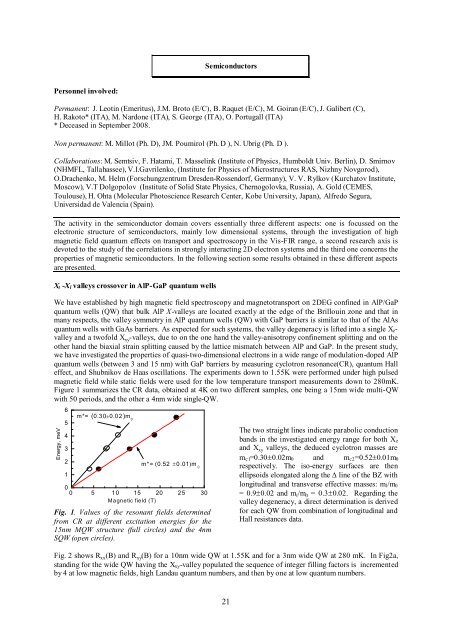
Figure 1 summarizes the CR data, obtained at 4K on two different samples, one being a 15nm wide multi-QW<br />
with 50 periods, and the other a 4nm wide single-QW.<br />
Energy, meV<br />
6<br />
5<br />
4<br />
3<br />
2<br />
1<br />
m*= (0.30�0.02 )m 0<br />
m*= (0.52 �0.01�m 0<br />
0<br />
0 5 10 15 20 25 30<br />
Magnetic field (T)<br />
Fig. 1. Values of the resonant fields determined<br />
from CR at different excitation energies for the<br />
15nm MQW structure (full circles) and the 4nm<br />
SQW (open circles).<br />
21<br />
The two straight lines indicate parabolic conduction<br />
bands in the investigated energy range for both Xz<br />
and X xy valleys, the deduced cyclotron masses are<br />
mc1=0.30�0.02m0 and mc2=0.52�0.01m0<br />
respectively. The iso-energy surfaces are then<br />
ellipsoids elongated along the �line of the BZ with<br />
longitudinal and transverse effective masses: ml/m0<br />
= 0.9�0.02 and m t/m 0 = 0.3�0.02. Regarding the<br />
valley degeneracy, a direct determination is derived<br />
for each QW from combination of longitudinal and<br />
Hall resistances data.<br />
Fig. 2 shows R xx(B) and R xy(B) for a 10nm wide QW at 1.55K and for a 3nm wide QW at 280 mK. In Fig2a,<br />
standing for the wide QW having the Xxy-valley populated the sequence of integer filling factors is incremented<br />
by 4 at low magnetic fields, high Landau quantum numbers, and then by one at low quantum numbers.