Modelling and Simulating the Selective Epitaxial Growth of ... - Imec
Modelling and Simulating the Selective Epitaxial Growth of ... - Imec
Modelling and Simulating the Selective Epitaxial Growth of ... - Imec

You also want an ePaper? Increase the reach of your titles
YUMPU automatically turns print PDFs into web optimized ePapers that Google loves.
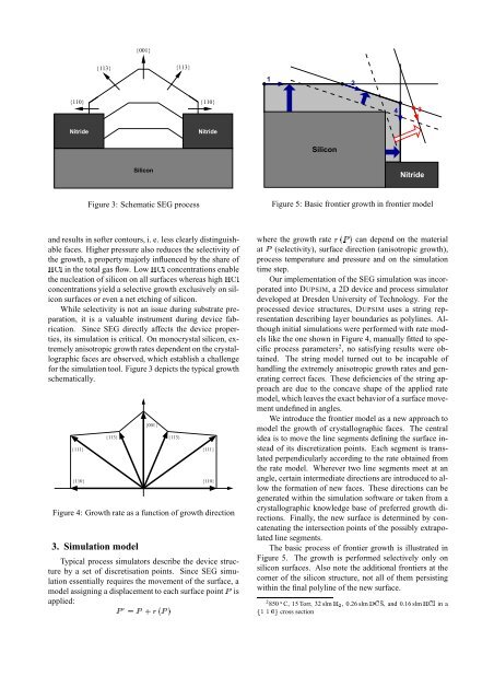
{110}<br />
{113}<br />
{001}<br />
Nitride Nitride<br />
Silicon<br />
{113}<br />
Figure 3: Schematic SEG process<br />
{110}<br />
<strong>and</strong> results in s<strong>of</strong>ter contours, i. e. less clearly distinguishable<br />
faces. Higher pressure also reduces <strong>the</strong> selectivity <strong>of</strong><br />
<strong>the</strong> growth, a property majorly influenced by <strong>the</strong> share <strong>of</strong><br />
§���� in <strong>the</strong> total gas flow. Low §���� concentrations enable<br />
<strong>the</strong> nucleation <strong>of</strong> silicon on all surfaces whereas high §����<br />
concentrations yield a selective growth exclusively on silicon<br />
surfaces or even a net etching <strong>of</strong> silicon.<br />
While selectivity is not an issue during substrate preparation,<br />
it is a valuable instrument during device fabrication.<br />
Since SEG directly affects <strong>the</strong> device properties,<br />
its simulation is critical. On monocrystal silicon, extremely<br />
anisotropic growth rates dependent on <strong>the</strong> crystallographic<br />
faces are observed, which establish a challenge<br />
for <strong>the</strong> simulation tool. Figure 3 depicts <strong>the</strong> typical growth<br />
schematically.<br />
{110}<br />
{113}<br />
{001}<br />
{113}<br />
{111} {111}<br />
{110}<br />
Figure 4: <strong>Growth</strong> rate as a function <strong>of</strong> growth direction<br />
3. Simulation model<br />
Typical process simulators describe <strong>the</strong> device structure<br />
by a set <strong>of</strong> discretisation points. Since SEG simulation<br />
essentially requires <strong>the</strong> movement <strong>of</strong> <strong>the</strong> surface, a<br />
model assigning a displacement to each surface point � is<br />
applied:<br />
�����������������<br />
1<br />
Silicon<br />
2<br />
4<br />
3<br />
Nitride<br />
Figure 5: Basic frontier growth in frontier model<br />
where <strong>the</strong> growth rate ������� can depend on <strong>the</strong> material<br />
at � (selectivity), surface direction (anisotropic growth),<br />
process temperature <strong>and</strong> pressure <strong>and</strong> on <strong>the</strong> simulation<br />
time step.<br />
Our implementation <strong>of</strong> <strong>the</strong> SEG simulation was incorporated<br />
into DUPSIM, a 2D device <strong>and</strong> process simulator<br />
developed at Dresden University <strong>of</strong> Technology. For <strong>the</strong><br />
processed device structures, DUPSIM uses a string representation<br />
describing layer boundaries as polylines. Although<br />
initial simulations were performed with rate models<br />
like <strong>the</strong> one shown in Figure 4, manually fitted to specific<br />
process parameters 2 , no satisfying results were obtained.<br />
The string model turned out to be incapable <strong>of</strong><br />
h<strong>and</strong>ling <strong>the</strong> extremely anisotropic growth rates <strong>and</strong> generating<br />
correct faces. These deficiencies <strong>of</strong> <strong>the</strong> string approach<br />
are due to <strong>the</strong> concave shape <strong>of</strong> <strong>the</strong> applied rate<br />
model, which leaves <strong>the</strong> exact behavior <strong>of</strong> a surface movement<br />
undefined in angles.<br />
We introduce <strong>the</strong> frontier model as a new approach to<br />
model <strong>the</strong> growth <strong>of</strong> crystallographic faces. The central<br />
idea is to move <strong>the</strong> line segments defining <strong>the</strong> surface instead<br />
<strong>of</strong> its discretization points. Each segment is translated<br />
perpendicularly according to <strong>the</strong> rate obtained from<br />
<strong>the</strong> rate model. Wherever two line segments meet at an<br />
angle, certain intermediate directions are introduced to allow<br />
<strong>the</strong> formation <strong>of</strong> new faces. These directions can be<br />
generated within <strong>the</strong> simulation s<strong>of</strong>tware or taken from a<br />
crystallographic knowledge base <strong>of</strong> preferred growth directions.<br />
Finally, <strong>the</strong> new surface is determined by concatenating<br />
<strong>the</strong> intersection points <strong>of</strong> <strong>the</strong> possibly extrapolated<br />
line segments.<br />
The basic process <strong>of</strong> frontier growth is illustrated in<br />
Figure 5. The growth is performed selectively only on<br />
silicon surfaces. Also note <strong>the</strong> additional frontiers at <strong>the</strong><br />
corner <strong>of</strong> <strong>the</strong> silicon structure, not all <strong>of</strong> <strong>the</strong>m persisting<br />
within <strong>the</strong> final polyline <strong>of</strong> <strong>the</strong> new surface.<br />
2 850 � C, 15 Torr, 32 slm ��� , 0.26 slm ����� , <strong>and</strong> 0.16 slm ����� in a<br />
��������� cross section