Modelling and Simulating the Selective Epitaxial Growth of ... - Imec
Modelling and Simulating the Selective Epitaxial Growth of ... - Imec
Modelling and Simulating the Selective Epitaxial Growth of ... - Imec

Create successful ePaper yourself
Turn your PDF publications into a flip-book with our unique Google optimized e-Paper software.
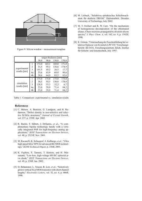
4a 3 4b<br />
1<br />
Figure 9: Silicon window – measurement template<br />
experimental<br />
results [nm]<br />
simulation<br />
results [nm]<br />
target thickness [nm]<br />
30,0 90,0 130,0 170,0<br />
1 173,0 165,1 169,0 171,0<br />
2 31,5 95,3 136,6 174,9<br />
3 141,5 45,2 26,5 17,7<br />
4a 23,6 63,9 69,8 80,6<br />
4b 20,6 64,9 83,5 82,6<br />
1 175,0 175,0 175,0 175,0<br />
2 30,5 93,5 136,0 178,0<br />
3 128,9 55,3 32,2 6,7<br />
4a 23,0 59,9 71,4 84,2<br />
4b 23,0 59,9 71,4 84,2<br />
Table 1: Comparison: experimental vs. simulation results<br />
References<br />
[1] C. Menon, A. Bentzen, G. L<strong>and</strong>gren, <strong>and</strong> H. Radamson,<br />
“Defect density in non-selective <strong>and</strong> selective<br />
Si/SiGe structures,” Journal <strong>of</strong> Crystal <strong>Growth</strong>,<br />
vol. 237, p. 259ff, Apr. 2002.<br />
[2] R. Bashir, F. Hébert, J. DeSantis, et al., “A complementary<br />
bipolar technology family with a vertically<br />
integrated PNP for high-frequency analog applications,”<br />
IEEE Transactions on Electron Devices,<br />
vol. 48, p. 2525ff, Nov. 2001.<br />
[3] M. Racanelli, K. Schuegraf, A. Kalburge, et al., “Ultra<br />
high speed SiGe NPN for advanced BiCMOS technology,”<br />
IEDM Technical Digest, p. 336ff, 2001.<br />
[4] K. Fujihira, S. Tamura, T. Kimoto, <strong>and</strong> H. Matsunami,<br />
“Low-loss, high-voltage 6H-SiC epitaxial pi-n<br />
diode,” IEEE Transactions on Electron Devices,<br />
vol. 49, p. 150ff, Jan. 2002.<br />
[5] D. Behammer, L. Vescan, R. Loo, et al., “<strong>Selective</strong>ly<br />
grown vertical Si-p MOS transistor with short channel<br />
lengths,” Electronics Letters, vol. 32, no. 4, p. 406ff,<br />
1996.<br />
2<br />
[6] M. Liebsch, “Selektives epitaktisches Schichtwachstum<br />
für skalierte DRAM,” Diplomarbeit, Dresden<br />
University <strong>of</strong> Technology, July 2002.<br />
[7] M. T. Swihart <strong>and</strong> R. W. Carr, “On <strong>the</strong> mechanism<br />
<strong>of</strong> homogeneous decomposition <strong>of</strong> <strong>the</strong> chlorinated<br />
silanes. Chain reactions propagated by divalent silicon<br />
species,” J. Phys. Chem. A, vol. 102, no. 9, p. 1542ff,<br />
1998.<br />
[8] K. Grimm, “Untersuchung der Facettenbildung bei selektiver<br />
Epitaxie von Si mittels LPCVD,” Forschungsbericht<br />
Jül-3416, Forschungszentrum Jülich, Institut<br />
für Schicht- und Ionentechnik, July 1997.