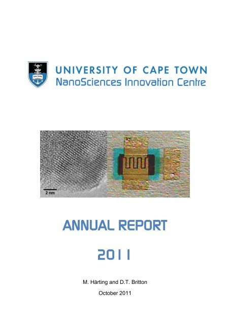
ANNUAL REPORT 2011 - University of Cape Town
ANNUAL REPORT 2011 - University of Cape Town
ANNUAL REPORT 2011 - University of Cape Town

You also want an ePaper? Increase the reach of your titles
YUMPU automatically turns print PDFs into web optimized ePapers that Google loves.
<strong>ANNUAL</strong> <strong>REPORT</strong><br />
<strong>2011</strong><br />
M. Härting and D.T. Britton<br />
October <strong>2011</strong>
Contents<br />
1. Introduction ......................................................................................................... 3<br />
1.1 Members and Affiliates ....................................................................................... 3<br />
2. An example <strong>of</strong> NanoSciences Innovation: Printed Silicon .............................. 4<br />
3. Activities <strong>of</strong> the NanoSciences Innovation Centre .......................................... 6<br />
3.1 Basic and Applied Research ............................................................................... 6<br />
3.1.1 Research Highlights in <strong>2011</strong> ............................................................................. 6<br />
3.1.2 Scientific Papers Published in <strong>2011</strong> .................................................................. 8<br />
3.2 Technology Development ................................................................................... 8<br />
3.2.1 Development Highlights in <strong>2011</strong> ....................................................................... 8<br />
3.2.2 Products and applications demonstrated in <strong>2011</strong> ............................................. 9<br />
3.3 Innovation ........................................................................................................... 10<br />
3.3.1 Provisional patents filed in <strong>2011</strong> ..................................................................... 10<br />
3.3.2 PCT patents filed in <strong>2011</strong> ............................................................................... 10<br />
3.3.3 National Phase patents filed in <strong>2011</strong> .............................................................. 11<br />
3.3.4 Patents granted in <strong>2011</strong> .................................................................................. 11<br />
3.4 Capacity Building and networking ....................................................................... 11<br />
3.4.1 Capacity building and networking highlights in <strong>2011</strong> ...................................... 11<br />
3.4.2 Current Students and Fellows......................................................................... 12<br />
3.4.3 Theses and Dissertations submitted in <strong>2011</strong> .................................................. 13<br />
3.4.4 Degrees passed in <strong>2011</strong> ................................................................................. 13<br />
4. Infrastructure and Capacity ............................................................................. 14<br />
4.1 External Use <strong>of</strong> Infrastructure in <strong>2011</strong> .............................................................. 15<br />
2
1. INTRODUCTION<br />
Recognising that innovation is an essential factor in turning cutting edge<br />
nanoscience research into practical nanotechnology applications, the UCT<br />
Nanosciences Innovation Centre was formally established in August 2010 as an<br />
accredited research centre in the Department <strong>of</strong> Physics. The centre has a strong<br />
focus on both basic research, with the generation <strong>of</strong> human resources and research<br />
capacity, and on innovation through its IP generation and support <strong>of</strong> its own spin-out<br />
companies. An example is its flagship project on the development <strong>of</strong> a printed silicon<br />
technology.<br />
The core values <strong>of</strong> the centre are: excellence in postgraduate education and<br />
research in the nanosciences; leadership in innovation, and the commercialisation <strong>of</strong><br />
nanosciences to locally based nanotechnology oriented companies. The centre’s<br />
primary function is to serve as an African hub for nanosciences research and<br />
postgraduate education with an orientation towards renewable energy and<br />
sustainable development. In the broader innovation landscape the other roles <strong>of</strong> the<br />
centre are to continue to develop its existing technology platforms, generate new<br />
intellectual property, and identify future applications.<br />
1.1 MEMBERS AND AFFILIATES<br />
Pr<strong>of</strong>. David T. Britton, Dept <strong>of</strong> Physics, <strong>University</strong> <strong>of</strong> <strong>Cape</strong> <strong>Town</strong>, Director:<br />
Capacity Building and Innovation<br />
Pr<strong>of</strong>. Margit Härting, Dept <strong>of</strong> Physics, <strong>University</strong> <strong>of</strong> <strong>Cape</strong> <strong>Town</strong>, Director:<br />
Capacity Research and Development<br />
Pr<strong>of</strong>. M. Bluemnthal, Dept. <strong>of</strong> Physics<br />
Dr. Schadrack Nsengiyumva, Dept <strong>of</strong> Physics, Rhodes <strong>University</strong><br />
Dr. Mira Topic, Materials Research Group, iThemba LABS<br />
Dr. Manfred R. Scriba, National Centre for Nanostructured Materials, CSIR<br />
Pr<strong>of</strong>. Girma Goro Gonfa, Haramaya <strong>University</strong>, Ethiopia<br />
Dr. Evariste Minani, Kigali Institute <strong>of</strong> Education, Rwanda<br />
Pr<strong>of</strong>. Gregory Beaucage, <strong>University</strong> <strong>of</strong> Cincinnati, USA<br />
3
1. AN EXAMPLE OF NANOSCIENCES INNOVATION:<br />
PRINTED SILICON<br />
Nanosciences innovation describes a holistic approach to all aspects <strong>of</strong> the<br />
innovation chain, shown in figure 1. below, concentrating mainly on the progression<br />
<strong>of</strong> an idea from basic research to pro<strong>of</strong> <strong>of</strong> concept. In the case <strong>of</strong> printed silicon our<br />
idea was simple: to print silicon nanoparticles on a substrate like paper to make<br />
electronic devices. The road to commercialising a product based on this idea<br />
required repeated review <strong>of</strong> the end goals in light <strong>of</strong> our research results and market<br />
developments. Eight years later the first product was commercialised, and we had<br />
developed our strategy <strong>of</strong> nanosciences innovation.<br />
Figure 1. The links in the Innovation Chain, showing the areas <strong>of</strong> activity <strong>of</strong> the<br />
NanoSciences Innovation Centre.<br />
With formulating an ink from silicon nanoparticles and printing electronics in a similar<br />
fashion to T-shirt printing, the printed silicon technology looks at first sight simple.<br />
But behind this process, shown in figure 2 below, a whole groundwork <strong>of</strong> basic<br />
science was needed to study and understand the properties <strong>of</strong> the materials. The<br />
results <strong>of</strong> these studies informed the direction <strong>of</strong> the applied research into the<br />
deposition <strong>of</strong> nanocomposite layers and the development <strong>of</strong> electronic devices,<br />
which were in turn guided by the requirements <strong>of</strong> the chosen application. Above all<br />
the final product was designed to make use <strong>of</strong> the unique and novel properties <strong>of</strong> the<br />
material system.<br />
4
Figure 2: Printed silicon technology: from silicon particles to printed electronic devices and circuits<br />
The key to the success <strong>of</strong> the technology lies in the quality <strong>of</strong> the surface <strong>of</strong> the<br />
silicon particles, which are clean enough to let electric charge pass between<br />
particles, but which are stable against oxidation. The second key, which opens up<br />
doors to many other applications which cannot be achieved with electronics<br />
technologies, is to understand and control the transport <strong>of</strong> electric charge through<br />
the printed silicon. In the end it is the understanding <strong>of</strong> its unique transport properties<br />
which allows printed silicon to be used, not only in sensor applications, but also in<br />
photovoltaics and logic.<br />
5
3. ACTIVITIES OF THE NANOSCIENCES INNOVATION<br />
CENTRE<br />
Until now the main research and development activities <strong>of</strong> the NanoSciences<br />
Innovation Centre were directed towards answering scientific questions related to the<br />
properties <strong>of</strong> nanoparticles and physical processes on the nanoscale, and to develop<br />
applications for its printed silicon technology. In continuing these tasks the centre is<br />
also turning its attention to exciting new applications, including combining the printed<br />
silicon technology with other nanomaterials, to develop for example robust solar cells<br />
for lighting and communications in rural areas <strong>of</strong> Africa with no access to grid power.<br />
As part <strong>of</strong> these activities the NanoSciences Innovation Centre is the primary hub <strong>of</strong><br />
the NanoPower Africa Network.<br />
3.1 Basic and Applied Research<br />
The core focus <strong>of</strong> our basic research is on the properties and interactions <strong>of</strong><br />
nanomaterials and nanostructured materials. We have a special emphasis on<br />
nanoparticles and nanoparticulate composites <strong>of</strong> electronic materials, specifically<br />
inorganic semiconductors like silicon. The goal is to understand the physical<br />
processes which occur, not only in the synthesis and fabrication <strong>of</strong> the material, but<br />
also in its application. A prime example <strong>of</strong> this is the generation and transport <strong>of</strong><br />
charge in the nanoparticle networks <strong>of</strong> printed silicon.<br />
The main goal <strong>of</strong> our applied research is to build on our successes in printed<br />
electronics to create an indigenous printable photovoltaic technology. This will<br />
ultimately provide robust solar cells which will bring inexpensive energy to rural<br />
areas <strong>of</strong> Africa which do not have access to grid power.<br />
Another important activity is the development <strong>of</strong> new fabrication and characterisation<br />
techniques, for which we have a well established long track record. Two important<br />
new developments, which will improve the quality <strong>of</strong> both product development and<br />
basic materials characterisation, are a novel synchrotron scattering technique to<br />
study the connectivity <strong>of</strong> nanoparticulate networks and tomographic reconstruction <strong>of</strong><br />
nanoparticle structures from electron micrographs.<br />
3.1.1 Research highlights in <strong>2011</strong><br />
The most important basic knowledge gained, which built on research started prior to<br />
the founding <strong>of</strong> the NanoSciences Innovation Centre, has been a comprehensive<br />
understanding <strong>of</strong> the functioning <strong>of</strong> the printed silicon technology at the level <strong>of</strong> the<br />
fundamental processes occurring at the interfaces between particles. This has three<br />
6
important aspects: firstly a study if the stable surface structure and composition <strong>of</strong><br />
silicon nanoparticles, secondly the factors influencing the hopping <strong>of</strong> charge carriers<br />
between particles and clusters, and finally the mesoscale influence <strong>of</strong> the network<br />
topology on the transport <strong>of</strong> charge.<br />
Silicon particle surfaces have now been studied extensively with further HR-TEM<br />
measurements (shown in figure 3), scanning near field optical microscopy and<br />
confocal Raman spectroscopy to supplement earlier X-ray photoelectron<br />
spectroscopy, confirming the reasons for the extraordinary surface stability. A<br />
substantial manuscript is currently being prepared for submission to a major<br />
interdisciplinary journal.<br />
Figure 3: HR-TEM image <strong>of</strong> a silicon nanoparticle showing the internal grain structure and the clean<br />
surface structure without a thick silicon dioxide layer.<br />
A wealth <strong>of</strong> experimental data, for the investigation <strong>of</strong> charge transfer mechanisms in<br />
nanoparticulate networks containing four different types <strong>of</strong> silicon nanoparticles, has<br />
been obtained over an extended temperature range from 15K to 350K. Consistent<br />
models for the hopping processes, and a description <strong>of</strong> the potential barriers,<br />
between individual particles and between clusters <strong>of</strong> particles, have been developed.<br />
This will form a major part <strong>of</strong> PhD thesis to be submitted early in 2012, and<br />
subsequently written up in series <strong>of</strong> papers for publication.<br />
In the framework <strong>of</strong> the NanoPower Africa project, in June 2012 members and<br />
students <strong>of</strong> the NanoSciences Innovation Centre performed the first Ultra Small<br />
angle X-ray scattering (USAXS) studies on this material system at the Advanced<br />
Photon Source in Argonne National Laboratory and Small Angle Neutron Scattering<br />
(SANS) studies at the High Flux Isotope Reactor (HFIR) at Oak Ridge National<br />
Laboratory. The results from the USAXS studies are being used with collaborators at<br />
the <strong>University</strong> <strong>of</strong> Cincinnati to jointly develop mathematical descriptions <strong>of</strong> the<br />
topology <strong>of</strong> the particle network, and to validate a new experimental technique based<br />
on the scattering nanometre wavelength radiation.<br />
In collaboration with the UCT Electron Microscope Unit, established electron<br />
tomographic methods have been further developed to apply them to reconstruct<br />
7
extended asymmetric structures, particularly irregular nanoparticles and polydisperse<br />
clusters <strong>of</strong> particles. The outcomes <strong>of</strong> this applied research are now being used to<br />
study basic features such as network topology, cluster morphology and particle<br />
topography in nanostructured materials.<br />
3.1.2 Scientific Papers published in <strong>2011</strong><br />
Oxygen depth pr<strong>of</strong>iling in Kr + -implanted polycrystalline alpha titanium by means <strong>of</strong><br />
16 O(�,�) 16 O resonance scattering,<br />
S. Nsengiyumva, J.P Rivière, A.T.Raji, C.M. Comrie, D.T. Britton, and M. Härting,<br />
Journal <strong>of</strong> Nuclear Materials 414, 150 – 155 (<strong>2011</strong>).<br />
Intrinsic defects and krypton impurity atoms in α-titanium: Ab initio density functional<br />
study <strong>of</strong> diffusion and krypton-vacancy interactions,<br />
A.T. Raji, R. Mazzarello, S. Scandolo, S. Nsengiyumva, M. Härting, D.T. Britton,<br />
Physical Review B 83, 054120 (<strong>2011</strong>)<br />
Electrically active, doped monocrystalline silicon nanoparticles produced by hot wire<br />
thermal catalytic pyrolysis,<br />
M. R. Scriba, D.T. Britton, and M. Härting<br />
Thin Solid Films, 519, 4491 – 4494 (<strong>2011</strong>)<br />
Defects in ion-implanted hcp-titanium: A first-principles study <strong>of</strong> electronic structures<br />
A.T. Raji, R. Mazzarello, S. Scandolo, S. Nsengiyumva, M. Härting, and D.T. Britton<br />
Solid State Communications, in press (<strong>2011</strong>)<br />
3.2 Technology Development<br />
Product and applications development in the NanoSciences Innovation Centre is<br />
currently focussed on the use <strong>of</strong> the printed silicon technology. Much <strong>of</strong> this is in<br />
collaboration with external partners, including PST Sensors, which is a spin-out from<br />
the Centre. Besides actively prototyping sensors and active electronics components,<br />
and manufacturing pro<strong>of</strong> <strong>of</strong> concept demonstrators, we are independently developing<br />
end-use applications for printed electronics, sensors and low power photovoltaics in<br />
various industrial and social sectors. A final, important aspect is the scaling up and<br />
industrialisation, also with external partners, <strong>of</strong> all the processes involved in the<br />
printed electronics value chain.<br />
3.2.1 Development Highlights in <strong>2011</strong><br />
In <strong>2011</strong>, in collaboration with PST Sensors the NanoSciences Innovation Centre has<br />
made several notable advances in the temperature sensor technology, since the first<br />
sensors (shown in figure 4 below) were exhibited at the <strong>2011</strong> Printed Electronics<br />
Europe Conference in Dusseldorf, Germany in April <strong>2011</strong>. At the conference and<br />
8
trade show, the NanoSciences Innovation Centre shared a booth with PST Sensors,<br />
and exhibited its other printed electronics developments, including transitors and<br />
passive components, as well as its research activities. The new developments,<br />
including strain compensation, allowing the production <strong>of</strong> fully flexible, rollable and<br />
even stretchable large area sensors, and sensor arrays for thermal mapping and<br />
imaging will be exhibited ate the Printed Electronics Conference USA in Santa Clara<br />
in December 2012.<br />
Throughout the year, development <strong>of</strong> printable electronic materials has continued<br />
with the successful production <strong>of</strong> graphitic nanoparticles which have been<br />
incorporated in water based inks for printed electronics. Basic research on the<br />
structure and properties <strong>of</strong> the graphitic nanoparticles is now ongoing and will<br />
continue in 2012. Following on from these successes, the first approaches to printing<br />
metallic nanoparticles, both as a replacement for conventional silver inks and to<br />
study the properties <strong>of</strong> printed Schottky barriers, have yielded encouraging results.<br />
Having demonstrated a working printed temperature sensor technology, the<br />
NanoSciences Innovation Centre is leading a consortium involving members <strong>of</strong><br />
Groote Schuur Hospital and the department <strong>of</strong> Human Biology to develop sensors<br />
for three specific medical applications. Preliminary results have shown that the<br />
sensors can be successfully used to monitor different aspects <strong>of</strong> health and bodily<br />
function, and ethical clearance is now being sought for a pilot study before<br />
submitting a proposal for major funding.<br />
3.2.2 Products and Applications demonstrated in <strong>2011</strong><br />
First fully printed temperature sensor, shown in figure 3, Printed Electronics<br />
Europe <strong>2011</strong>, Dusseldorf, Germany in April <strong>2011</strong><br />
Figure 4: Printed Silicon Temperature Sensor, developed by the UCT NanoSciences Innovation<br />
Centre and commercialised by PST Sensors (pty) Ltd.<br />
9
Large area temperature sensor in form <strong>of</strong> life size hand graphic design, Printed<br />
Electronics Europe <strong>2011</strong>, Dusseldorf, Germany in April <strong>2011</strong><br />
Temperature sensor arrays for thermal mapping, Printed Electronics USA 2012,<br />
Santa Clara, 30th November – 1st December <strong>2011</strong><br />
Strain compensated flexible temperature sensor, Printed Electronics USA 2012,<br />
Santa Clara, 30th November – 1st December <strong>2011</strong><br />
Temperature sensors, using inexpensive copper based inks as a replacement<br />
for silver, Printed Electronics USA 2012, Santa Clara, 30th November – 1st<br />
December <strong>2011</strong><br />
3.3 Innovation<br />
The NanoSciences Innovation Centre has a strong track record in Intellectual<br />
Property generation, with 14 patent families filed . Of these, two patents have been<br />
granted in the United States, two in Europe, and 3 in South Africa. Shortly after the<br />
formal establishment <strong>of</strong> the Centre, the first South Africa second generation<br />
nanotechnology company in the electronics sector, PST Sensors, was spun out.<br />
Besides working with its own daughter company, The NanoSciences Innovation<br />
Centre is engaging with other partners for commercial prototyping, leading to<br />
licensing agreements for its intellectual property.<br />
3.3.1 Provisional patents filed in <strong>2011</strong><br />
A Method <strong>of</strong> Producing Nanoparticles<br />
M.R Scriba and DT Britton<br />
Flexible temperature and strain sensor<br />
D.T. Britton and M. Härting<br />
Large area temperature sensors<br />
D.T. Britton and M. Härting<br />
Printed semiconductor diodes,<br />
M. Härting, D.T. Britton and U. Männl<br />
3.3.2 PCT patents filed in <strong>2011</strong><br />
Assembling and Packaging a Discrete Electronic Component<br />
D.T. Britton and M Härting,<br />
Printed Temperature Sensor<br />
D.T. Britton and M Härting<br />
10
3.3.3 National Phase patents filed in <strong>2011</strong><br />
Inkjet Printing <strong>of</strong> Nanoparticulate Functional Inks<br />
M. Härting, D.T. Britton and E.A. Odo<br />
Russia<br />
Method <strong>of</strong> Producing Stable Oxygen Terminated Semiconducting Nanoparticles<br />
D.T. Britton and M. Härting<br />
Russia<br />
3.3.4 International Patents granted in <strong>2011</strong><br />
A Thin Film Semiconductor Device and Method <strong>of</strong> Manufacturing a Thin Film<br />
Semiconductor Device,<br />
M. Härting and D.T. Britton<br />
US 8026565 USA<br />
Doping <strong>of</strong> Particulate Semiconductor Materials<br />
D.T. Britton and M. Härting<br />
EP 1926843 European<br />
Inkjet Printing <strong>of</strong> Nanoparticulate Functional Inks<br />
M. Härting, D.T. Britton and E.A. Odo<br />
EP 2285574 European<br />
3.4 Capacity building and networking<br />
As a university based research centre, our main contribution to human capacity<br />
building is the training <strong>of</strong> Masters and Doctoral students at the cutting edge <strong>of</strong><br />
nanosciences research. Over the last 10 years we have graduated a total <strong>of</strong> 15 MSc<br />
and 8 PhD students. However, with second focus on innovation and<br />
commercialisation, there is excellent mentoring and opportunities for students who<br />
make a more adventurous life choice – entrepreneurship. Additionally, as the primary<br />
hub <strong>of</strong> an international capacity building network, NanoPower Africa, we are actively<br />
involved in similar activities in four countries on the continent.<br />
3.4.1 Capacity Building and Networking Highlights in <strong>2011</strong><br />
The NanoPower Africa network was formally founded with the start <strong>of</strong> the USAID<br />
funded project on 28 th February. However, its first activities commenced in the<br />
second half <strong>of</strong> <strong>2011</strong> after all contractual issues between UCT and the US partner<br />
institutions had been ironed out. The first significant activities were site visits by the<br />
11
coordinating team to the first two other African partner institutions in Rwanda and<br />
Ethiopia. Key outcomes <strong>of</strong> these visits were the planning <strong>of</strong> research visits to <strong>Cape</strong><br />
<strong>Town</strong> and the USA by the senior members <strong>of</strong> the institutions, and the identification <strong>of</strong><br />
junior staff members who will join the NanoSciences Innovation Centre as<br />
postgraduate students. Two junior staff members from each institution were<br />
identified and have applied to UCT for first registration in 2012. Similarly, after the<br />
first release <strong>of</strong> funds, recruitment <strong>of</strong> support and scientific staff, as well as local<br />
postgraduate students for 2012 has been initiated in the second semester <strong>of</strong> <strong>2011</strong>. In<br />
total the postgraduate student cohort <strong>of</strong> the NanoSciences Innovation Centre is<br />
expected to double from its mid-<strong>2011</strong> number by April 2012.<br />
This planned growth is enabled by the addition <strong>of</strong> new partners in the NanoPower<br />
Africa network and the affiliation <strong>of</strong> locally based collaborators to the NanoSciences<br />
Innovation Centre. Since its inception, new partners in at Rhodes <strong>University</strong> in South<br />
Africa, and the <strong>University</strong> <strong>of</strong> Botswana and BOTEC in Gaberone, have joined the<br />
NanoPower Africa Network. Within South Africa, the NanoSciences Innovation<br />
Centre is consolidating its own network with affilates at other universities and<br />
research institutions, including the CSIR National Centre for Nanostructured<br />
Materials and iThemba LABS. Similarly, within the Department <strong>of</strong> Physics, associate<br />
Pr<strong>of</strong>essor Mark Blumenthal is the newest member <strong>of</strong> the NanoSciences Innovation<br />
Centre.<br />
As part <strong>of</strong> the USAID funded initiative, the members <strong>of</strong> the NanoSciences Innovation<br />
Centre have been instrumental in implementing an experimental lecture series held<br />
simultaneously at six sites, in four countries on two continents. The assistance <strong>of</strong><br />
UCT’s Health Science Faculty in providing essential infrastructure has been<br />
invaluable in this regard. As part <strong>of</strong> this programme, African science and engineering<br />
postgraduate students are expected to work with Amercian social and business<br />
science undergraduate students, assisting them in understanding and developing<br />
appropriate business models for solar power projects the different African countries.<br />
As part <strong>of</strong> our involvement in USAID activities, a low key working visit by Dr. John. P.<br />
Holdren, Director <strong>of</strong> the White House Office <strong>of</strong> Science and TechnologyPolicy, and<br />
Assistant to the Preseident for Science and Technology, is planned for 11 th<br />
November <strong>2011</strong>.<br />
3.4.2 Current Students and Fellows<br />
MSc<br />
David Moweme Unuigbe<br />
Lehlohonolo Mongalo<br />
Michel Mambouku Nzikou<br />
Sara Abdelazeem Hassan Abass<br />
12
PhD<br />
Lloyd Angelo Corker (under examination)<br />
Emmanuel Ohieku Jonah<br />
Batsirai Magunje<br />
Stanley Douglas Walton<br />
Stephen David Jones<br />
Ulrich Männl<br />
Post-doctoral<br />
Abdulrafiu Tunde Raji<br />
Rudolf Nüssl<br />
3.4.3 Student Theses and Dissertations Submitted in <strong>2011</strong><br />
Lloyd Angelo Corker, PhD<br />
Lehlohonolo Mongalo, MSc<br />
3.4.4 Degrees passed in <strong>2011</strong><br />
Sara Abdelazeem Hassan Abass, MSc<br />
Michel Nzikou, MSc<br />
13
4. INFRASTRUCTURE AND CAPACITY<br />
The NanoSciences Innovation Centre is currently housed in the Physics Department<br />
at the <strong>University</strong> <strong>of</strong> <strong>Cape</strong> <strong>Town</strong>, where the available space is not optimal for its<br />
extensive equipment infrastructure. However, it is expected that more suitable<br />
accommodation will become available in late 2012.<br />
In-house equipment includes the following state <strong>of</strong> the art laboratory scale<br />
characterisation facilities, as well as all the requirements <strong>of</strong> a well-found laboratory:<br />
Spire Spi Cell AM1.5 solar cell tester (figure 5 left), Lake Shore 7700 cryogenic Hall<br />
measurement system, Keithley 4200 semiconductor characterisation system, Wyko<br />
NT9100 optical pr<strong>of</strong>iler (figure 5 right, a unique facility in Africa), and a Delta Nu<br />
Advance 532 Raman spectrometer. Other in-house equipment includes printing and<br />
deposition equipment, such as an Atma 60PD semi automatic screen printer, and<br />
sample preparation facilities. Besides being used in house, the characterisation<br />
facilities <strong>of</strong> the centre are regularly used by staff and students from all three local<br />
universities and iThemba LABS.<br />
Access to major equipment is provided through the <strong>University</strong> <strong>of</strong> <strong>Cape</strong> <strong>Town</strong> and<br />
external collaborations, including the NanoPower Africa Network <strong>of</strong> which Oak Ridge<br />
National Laboratory and Argonne National Laboratory are partners, which<br />
guarantees access to synchrotron and neutron scattering experiments. High<br />
resolution transmission and scanning electron microscopy is available on site in the<br />
neighbouring UCT Electron Microsocope Unit.<br />
Figure 5: State <strong>of</strong> the art equipment in the NanoSciences Innovation Centre: Spire SPI CELL solar cell tester<br />
(left) and Wyko NT9100 Optical Pr<strong>of</strong>iler (right)<br />
14
4.1 External Use <strong>of</strong> Infrastructure in <strong>2011</strong><br />
Wyko NT9100 pr<strong>of</strong>iler: Dept <strong>of</strong> Mechanical Engineering, UCT<br />
iThemba LABS<br />
<strong>University</strong> <strong>of</strong> the Western <strong>Cape</strong><br />
Raman Spectrometer: Dept. <strong>of</strong> Human Biology, UCT<br />
<strong>University</strong> <strong>of</strong> the Western <strong>Cape</strong><br />
<strong>University</strong> <strong>of</strong> Stellenbosch<br />
Lake Shore 7700 HMS: Dept <strong>of</strong> Mechanical Engineering, UCT<br />
iThemba LABS<br />
<strong>University</strong> <strong>of</strong> Stellenbosch<br />
15