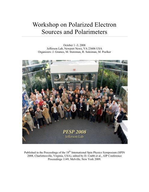
Workshop on Polarized Electron Sources and Polarimeters
Workshop on Polarized Electron Sources and Polarimeters
Workshop on Polarized Electron Sources and Polarimeters

You also want an ePaper? Increase the reach of your titles
YUMPU automatically turns print PDFs into web optimized ePapers that Google loves.
<str<strong>on</strong>g>Workshop</str<strong>on</strong>g> <strong>on</strong> <strong>Polarized</strong> Electr<strong>on</strong><br />
<strong>Sources</strong> <strong>and</strong> <strong>Polarimeters</strong><br />
October 1 -3, 2008<br />
Jeffers<strong>on</strong> Lab, Newport News, VA 23606 USA<br />
Organizers: J. Grames, M. Stutzman, R. Suleiman, M. Poelker<br />
Published in the Proceedings of the 18 th Internati<strong>on</strong>al Spin Physics Symposium (SPIN<br />
2008, Charlottesville, Virginia, USA), edited by D. Crabb et al., AIP C<strong>on</strong>ference<br />
Proceedings 1149, Melville, New York 2009.
<str<strong>on</strong>g>Workshop</str<strong>on</strong>g> <strong>on</strong> <strong>Polarized</strong> Electr<strong>on</strong> <strong>Sources</strong><br />
<strong>and</strong> <strong>Polarimeters</strong><br />
Status Report of the New Darmstadt <strong>Polarized</strong> Electr<strong>on</strong> Injector…<br />
Y. Poltoratska, R. Barday, U. B<strong>on</strong>nes, M. Brunken, C. Eckardt,<br />
R. Eichhorn, J. Enders, C. Heßler, C. Ingenhaag, W. F. O. Müller,<br />
M. Platz, M. Roth, B. Steiner, M. Wagner, <strong>and</strong> T. Weil<strong>and</strong> - Page 983<br />
Status of 200keV Beam Operati<strong>on</strong>s at Nagoya University ….<br />
M. Yamamoto, T. K<strong>on</strong>omi, S. Okumi, Y. Nakagawa,<br />
N. Yamamoto, M. Tanioku, X. Jin, T. Ujihara, Y. Takeda,<br />
F. Furuta, H. Matsumoto, M. Yoshioka, M. Kuriki, C. Sh<strong>on</strong>aka, <strong>and</strong> T. Nakanishi -<br />
Page 987<br />
Recent <strong>Polarized</strong> Photocathode R&D at SLAC <strong>and</strong> Future Plans…<br />
F. Zhou, A. Brachmann, T. Maruyama, <strong>and</strong> J. C. Sheppard - Page 992<br />
High Intensity <strong>Polarized</strong> Electr<strong>on</strong> Gun Studies at MIT-Bates…<br />
E. Tsentalovich - Page 997<br />
Atomic Hydrogen Cleaning of Superlattice Cathodes….<br />
V. Tioukine, K. Aulenbacher, <strong>and</strong> E. Riehn - Page 1002<br />
Ultra Cold Photoelectr<strong>on</strong> Beams for I<strong>on</strong> Storage Rings….<br />
D. A. Orlov, C. Krantz, A. Shornikov, M. Lestinsky,<br />
J. Hoffmann, A.S. Jaroshevich, S.N. Kosolobov,<br />
A.S. Terekhov, <strong>and</strong> A. Wolf - Page 1007<br />
Optimizati<strong>on</strong> of Semic<strong>on</strong>ductor Superlattice for Spin-<strong>Polarized</strong> Electr<strong>on</strong> Source…<br />
L. G. Gerchikov, Yu. A. Mamaev, V. V. Kuz’michev, Yu. P.Yashin, V. S. Mikhrin,<br />
A. P. Vasiliev, <strong>and</strong> A. E. Zhukov - Page 1017<br />
Study of the Activated GaAs Surface for Applicati<strong>on</strong> as an Electr<strong>on</strong> Source in<br />
Particle Accelerators…<br />
N. Chanlek, J.D. Herbert, L.B. J<strong>on</strong>es, R.M. J<strong>on</strong>es, <strong>and</strong><br />
K.J. Middleman - Page 1022<br />
Recent Progress toward Robust Photocathodes…<br />
G. A. Mulhollan <strong>and</strong> J. C. Bierman - Page 1027
Surface Analysis of Damaged Superlattice Photocathode…<br />
M. L. Stutzman <strong>and</strong> J. Grames - Page 1032<br />
<strong>Polarized</strong> Photocathode Development at SVT Associates….<br />
Aar<strong>on</strong> Moy, T. Maruyama, F. Zhou <strong>and</strong> A. Brachmann - Page 1038<br />
High Brightness Electr<strong>on</strong> Source Using a Superlattice Photocathode with L<strong>on</strong>g Life<br />
NEA-Surface….<br />
T. Nishitani, M. Tabuchi, Y. Takeda, Y. Suzuki, K. Motoki, <strong>and</strong><br />
T. Meguro – Page 1047<br />
High Brightness <strong>and</strong> High Polarizati<strong>on</strong> Electr<strong>on</strong> Source Using Transmissi<strong>on</strong><br />
Photocathode…<br />
N. Yamamoto, X. Jin, A. Mano, Y. Nakagawa, T. Nakanishi,<br />
T. Ujihara, S. Okumi, M. Yamamoto, T. K<strong>on</strong>omi, Y. Takeda,<br />
T. Ohshima, T. Saka, T. Kato, H. Horinaka, T. Yasue, <strong>and</strong><br />
T. Koshikawa – Page 1052<br />
Cooled Transmissi<strong>on</strong>-Mode NEA-Photocathode with B<strong>and</strong>-Graded Active Layer for<br />
High–Brightness Electr<strong>on</strong> Source…<br />
L. B. J<strong>on</strong>es, S. A. Rozhkov, V. V. Bakin, S. N. Kosolobov,<br />
B. L. Militsyn, H. E. Scheibler. S. L. Smith, <strong>and</strong> A. Terekhov - Page 1057<br />
K2CsSb Photocathodes…<br />
John Smedley, Triveni Rao, <strong>and</strong> E. Wang - Page 1062<br />
Photoemissi<strong>on</strong> Spectroscopic Study of Cesium Telluride Thin Film Photocathode…<br />
H., K. Ogawa, Junpei Azuma, K. Takahashi, <strong>and</strong> M. Kamada - Page 1067<br />
Status Jeffers<strong>on</strong> Lab FEL High Voltage Guns…<br />
C. Hern<strong>and</strong>ez-Garcia, S. V. Bens<strong>on</strong>, G. Biallas, D. Bullard,<br />
P. Evtushenko, K. Jordan, M. Klopf, D. Sext<strong>on</strong>, C. Tennant,<br />
R. Walker, <strong>and</strong> G. Williams - Page 1071<br />
Status Cornell High Voltage Gun…<br />
K. Smolenski, I. Bazarov, B. Dunham, H. Li, Y. Li, X. Liu,<br />
D. Ouzounov, <strong>and</strong> C. Sinclair - Page 1077<br />
Status of the ALICE Energy-Recovery Linac…<br />
L. J<strong>on</strong>es, S. P. Jamis<strong>on</strong>, Y. M. Saveliev, K. J. Middleman, <strong>and</strong><br />
S. L. Smith - Page 1084
Photocathode Preparati<strong>on</strong> System for the ALICE Photoinjector Gun…<br />
K. J Middleman, I. Burrows, R. Cash, B. Fell, L.B. J<strong>on</strong>es,<br />
J. McKenzie, B. Militsyn, <strong>and</strong> A.S. Terekhov - Page 1089<br />
Development of an Electr<strong>on</strong> Gun for an ERL Based Light Source in Japan…<br />
N. Nishimori, R. Nagai, H. Iijima, Y. H<strong>on</strong>da, T. Muto, M. Kuriki, M Yamamoto, S.<br />
Okumi, T. Nakanishi, <strong>and</strong> R. Hajima - Page 1094<br />
KSI's Cross Insulated Core Transformer Technology…<br />
Uwe Uhmeyer - Page 1099<br />
Low Emittance Gun for XFEL Applicati<strong>on</strong>…<br />
C. Gough, M. Paraliev <strong>and</strong> S. Ivko - Page 1104<br />
I<strong>on</strong> Bombardment in RF Guns: Analytical Approach…<br />
E. Pozdeyev, D. Kayran, <strong>and</strong> V. N. Litvinenko - Page 1109<br />
High-Fidelity RF Gun Simulati<strong>on</strong>s with the Parallel 3D Finite Element Particle-In-<br />
Cell Code Pic3P…<br />
A. C<strong>and</strong>el, A. Kabel, L. Lee, Z. Li, C. Limborg, C. Ng,<br />
G. Schussman, <strong>and</strong> K. Ko - Page 1114<br />
The Superc<strong>on</strong>ducting RF Photoinjector at Elbe – First Operati<strong>on</strong>al Experience…<br />
J. Teichert, A. Arnold, H. Büttig, D. Janssen, M. Justus,<br />
U. Lehnert, P. Michel, P. Murcek, A. Schamlott, C. Schneider,<br />
R. Schurig, F. Staufenbiel, R. Xiang, T. Kamps, J. Rudolph, M. Schenk, G. Klemz,<br />
<strong>and</strong> I. Will - Page 1119<br />
Measurements of the Rossendorf SRF-Gun Cavity Characteristics…<br />
A. Arnold, H. Büttig, D. Janssen, M. Justus, T. Kamps, G. Klemz,<br />
U. Lehnert, P. Michel, K. Möller, P. Murcek, J. Rudolph,<br />
A. Schamlott, M. Schenk, Ch. Schneider, R. Schurig,<br />
F. Staufenbiel, J. Teichert, V. Volkov, I. Will, <strong>and</strong> R. Xiang - Page 1125<br />
The BNL <strong>Polarized</strong> SRF gun…<br />
J. Kewisch, I. Ben-Zvi, T. Rao, A. Burril, D. Pate, E. Wang,<br />
R. Todd, H. Bluem, D. Holmes, <strong>and</strong> T. Schultheiss - Page 1133<br />
NEG Pump Technology…<br />
P. Manini - Page 1138<br />
Ultrahigh Vacuum I<strong>on</strong> Pump Power Supply with Sensitive Current M<strong>on</strong>itoring<br />
Capability…<br />
J. Hansknecht, P. Adderley, M. L. Stutzman <strong>and</strong> M. Poelker - Page 1143
High Brightness <strong>and</strong> High Polarizati<strong>on</strong> PES for SPLEEM <strong>and</strong>/or High Brightness<br />
PES with Transmissi<strong>on</strong> Photocathode…<br />
T. Nakanishi, N. Yamamoto, A. Mano, Y. Nakagawa, T. K<strong>on</strong>omi,<br />
M. Yamamoto, S. Okumi, X. Jin, T. Ujihara, Y. Takeda,<br />
T. Ohshima, T. Kohashi, T. Yasue, T. Koshikawa, T. Saka, <strong>and</strong><br />
T. Kato - Page 1148<br />
Ab Initio Calculati<strong>on</strong> of Effective Sherman Functi<strong>on</strong> in MeV Mott Scattering…<br />
K. Aulenbacher <strong>and</strong> V. Tioukine - Page 1155<br />
Compt<strong>on</strong> Polarimeter at B<strong>on</strong>n….<br />
W. Hillert, B. Aur<strong>and</strong>, <strong>and</strong> J. Wittschen - Page 1160<br />
Hall A Compt<strong>on</strong> Polarimeter – DC Green Light <strong>and</strong> Optical Storage Cavity…<br />
A. Rakhman, S. N<strong>and</strong>a, P. Souder - Page 1165<br />
Polarimetry <strong>and</strong> Planned Experiments at the Superc<strong>on</strong>ducting Darmstadt Electr<strong>on</strong><br />
Linac S-DALINAC…<br />
C. Eckardt, R. Barday, U. B<strong>on</strong>nes, M. Brunken, R. Eichhorn,<br />
J. Enders, C. Heßler, W. F. O. Müller, M. Platz, Y. Poltoratska, B. Steiner, M.<br />
Wagner, <strong>and</strong> T. Weil<strong>and</strong> - Page 1170<br />
Benchmark Studies Am<strong>on</strong>g Own <strong>and</strong> Commercial Beam Tracking Codes <strong>on</strong><br />
Fundamental C<strong>on</strong>diti<strong>on</strong>s…<br />
N. Yamamoto, A. Mizuno, K. Masuda, K. Kan, S. Matsumoto, <strong>and</strong><br />
M. Yamamoto - Page 1174<br />
3D Modeling of the ALICE Photoinjector Upgrade…<br />
J.W. McKenzie, B.L. Militsyn, <strong>and</strong> Y.M. Saveliev - Page 1179<br />
<strong>Polarized</strong> Positr<strong>on</strong> Source at Jeffers<strong>on</strong> Lab….<br />
J. Dumas, J. Grames, E. Voutier - Page 1184<br />
Summary Report of PESP2008 -The <str<strong>on</strong>g>Workshop</str<strong>on</strong>g> <strong>on</strong> <strong>Polarized</strong> Electr<strong>on</strong>s <strong>and</strong><br />
<strong>Polarimeters</strong>….<br />
M. Poelker - Page 1189
Status Report of the New Darmstadt <strong>Polarized</strong><br />
Electr<strong>on</strong> Injector<br />
Y. Poltoratska ∗ , R. Barday ∗ , U. B<strong>on</strong>nes ∗ , M. Brunken ∗ , C. Eckardt ∗ ,R.<br />
Eichhorn ∗ , J. Enders ∗ , C. Heßler ∗ , C. Ingenhaag ∗ , W.F.O. Müller † ,M.<br />
Platz ∗ , M. Roth ∗ , B. Steiner † , M. Wagner ∗ <strong>and</strong> T. Weil<strong>and</strong> †<br />
∗ Institut für Kernphysik, Technische Universität Darmstadt, Germany<br />
† Institut für Theorie Elektromagnetischer Felder, Technische Universität Darmstadt, Germany<br />
Abstract. We present the status of the polarized injector for the superc<strong>on</strong>ducting Darmstadt electr<strong>on</strong><br />
linear accelerator S-DALINAC. An offline testst<strong>and</strong> of the source was built to test all comp<strong>on</strong>ents<br />
of the S-DALINAC polarized injector SPIN. The new electr<strong>on</strong> source will deliver a 100 keV<br />
polarized beam <strong>and</strong> complement the present thermi<strong>on</strong>ic source operating at 250 kV. Results of the<br />
beam properties measurements will be introduced <strong>and</strong> an outlook <strong>on</strong> the upcoming installati<strong>on</strong> of<br />
the new injector at the S-DALINAC will be given.<br />
Keywords: S-DALINAC, strained superlattice GaAs, Mott polarimeter, Wien filter<br />
PACS: 85.60.Ha, 79.60.-i, 29.27.Hj<br />
INTRODUCTION<br />
The superc<strong>on</strong>ducting Darmstadt electr<strong>on</strong> linear accelerator S-DALINAC [1] is <strong>on</strong>e of<br />
very few electr<strong>on</strong> accelerators devoted to nuclear structure physics, including electr<strong>on</strong>scattering<br />
experiments. To complement the present scientific programm with the experiments<br />
that are focused <strong>on</strong> the investigati<strong>on</strong> of violati<strong>on</strong> of parity in the nuclei <strong>and</strong><br />
breakup reacti<strong>on</strong>s of light nuclei [2] the new S-DALINAC <strong>Polarized</strong> injector (SPIN)<br />
was designed. It will provide - complementary to the existing 250 kV thermi<strong>on</strong>ic electr<strong>on</strong><br />
gun 100 keV polarized beams with polarizati<strong>on</strong> of 80 %, a mean current of 60 µA<br />
<strong>and</strong> 3 GHz cw or subharm<strong>on</strong>ic time structure. The c<strong>on</strong>cept of the MAMI Gun [3] was<br />
used as a starting point for SPIN. To test the new developed polarized electr<strong>on</strong> source<br />
independently from the operati<strong>on</strong> of the S-DALINAC, an st<strong>and</strong>al<strong>on</strong>e testst<strong>and</strong> has been<br />
developed. In this c<strong>on</strong>tributi<strong>on</strong> we describe the current status of the testst<strong>and</strong> <strong>and</strong> present<br />
the results of the measurements of the different beam properties.<br />
TEST STAND OF THE POLARIZED INJECTOR<br />
Figure 1 shows an schematic overview over the testst<strong>and</strong> of the polarized injector. The<br />
electr<strong>on</strong>s are produced at a GaAs cathode by photoemissi<strong>on</strong>. As cathode material the<br />
strained superlattice crystals [4] are foreseen to achieve high degrees of polarizati<strong>on</strong> of<br />
more than 80%. Due to the limited space in the accelerator hall a very compact source<br />
had to be c<strong>on</strong>structed, <strong>and</strong> major modificati<strong>on</strong>s from the Mainz design were necessary.<br />
One spin directi<strong>on</strong> is selected by using circularly polarized light from diode laser system
FIGURE 1. Schematic drawing of the testst<strong>and</strong>.<br />
below the electr<strong>on</strong> source focussed <strong>on</strong>to the photocathode surface. The photocathode<br />
crystal is installed at the fr<strong>on</strong>t end of a highly polished stainless-steel electrode. The<br />
form of the electrode was designed following numerical simulati<strong>on</strong>s [5] <strong>and</strong> deviates<br />
from usual Pierce geometry [6]. To extract the electr<strong>on</strong>s from the c<strong>on</strong>ducti<strong>on</strong> b<strong>and</strong> of<br />
the cathode crystal to the vacuum negative electr<strong>on</strong> affinity (NEA) is needed. Therefore<br />
prior to installati<strong>on</strong> into the cathode chamber the cathode is cleaned <strong>and</strong> activated by<br />
depositing thin CsO layer in a separate preparati<strong>on</strong> chamber. With the aid of a load-lock<br />
system the photocathode activati<strong>on</strong> can be h<strong>and</strong>led quickly.<br />
Afterwards the emitted electr<strong>on</strong>s are accelerated electrostatically to an energy of<br />
100 keV <strong>and</strong> injected by an alpha magnet into a horiz<strong>on</strong>tal beamline, where the beam<br />
properties are measured with various diagnostic elements. It is indispensable to create<br />
an ultra high vacuum c<strong>on</strong>diti<strong>on</strong>s in the gun chamber to prevent a fast degradati<strong>on</strong><br />
of the NEA surface. After bake-out during 12 days at 220 ◦ C an end pressure of<br />
< 2 · 10 −11 mbar has been achieved using n<strong>on</strong>-evaporable getter (NEG) <strong>and</strong> i<strong>on</strong>-getter<br />
pumps.<br />
Transverse beam quality<br />
The transverse beam properties can be investigated qualitatively by fluorescent<br />
screens <strong>and</strong> quantitatively by a wire scanner [7]. The transverse emittance is determined<br />
by measuring of the beam radius for different focussing strengths of a solenoid preceding<br />
the wire scanner. The normalized transverse emittance has been determined to<br />
εn,x =(0.146 ± 0.037) mm mrad <strong>and</strong> εn,y =(0.197 ± 0.089) mm mrad, respectively.<br />
Time Structure<br />
The produced polarized electr<strong>on</strong> beam needs to be modulated with the frequency of<br />
the S-DALINAS’s superc<strong>on</strong>ducting cavities of 3 GHz for cw operati<strong>on</strong>. This is achieved<br />
by modulating a laser diode [8]. The time structure was verified for the laser beam
with a fast sensor <strong>and</strong> for the electr<strong>on</strong> beam with an ultra-fast coaxial Faraday cup.<br />
For the capturing process of the beam into the superc<strong>on</strong>ducting accelerating structures<br />
the electr<strong>on</strong>-bunch length need to be of the order of 5 ps. Therefore a new chopper <strong>and</strong><br />
prebuncher system has been developed, based <strong>on</strong> a similar setup at MAMI [9].<br />
Polarizati<strong>on</strong> manipulati<strong>on</strong> <strong>and</strong> measurement<br />
The degree of polarizati<strong>on</strong> of 100 keV electr<strong>on</strong>s for the testst<strong>and</strong> is measured with a<br />
Mott polarimeter detecting count-rate asymmetries in electr<strong>on</strong> scattering <strong>on</strong> nuclei due<br />
to the spin-orbit interacti<strong>on</strong>. The asymmetry occurs <strong>on</strong>ly when the electr<strong>on</strong> spin directi<strong>on</strong><br />
is not parallel to the scattering plane. Thus the initially l<strong>on</strong>gitudinal oriented spins must<br />
be rotated by 90 ◦ into the transverse directi<strong>on</strong>. This is d<strong>on</strong>e by a Wien filter [10]. This<br />
device is also necessary tool for adjusting the spin orientati<strong>on</strong> at different experimental<br />
areas of the S-DALINAC.<br />
The ideal Wien filter acts as a drift space in the vertical plane, but its horiz<strong>on</strong>tal<br />
electr<strong>on</strong>-optical properties are similar to those of a quadrupole: It focusses the electr<strong>on</strong><br />
beam. This effect was minimized: the focus has been set inside the filter with help of<br />
newly designed compact quadrupole triplet in fr<strong>on</strong>t of the Wien filter. An additi<strong>on</strong>al<br />
quadrupole doublet installed after the device compensates its influence <strong>on</strong> the beam.<br />
The installed spin rotator can provide 100 degree spin rotati<strong>on</strong>.<br />
The 100 keV Mott polarimeter [11] houses 4 silic<strong>on</strong>-surface-barrier detectors which<br />
are oriented in two perpendicular scattering planes to measure both transverse polarizati<strong>on</strong><br />
comp<strong>on</strong>ents simultaneously. As targets self-supporting gold foils of the thickness<br />
in the range from 42.5 nm to 500 nm are utilized. The polarimeter c<strong>on</strong>tains also a BeO<br />
viewer to c<strong>on</strong>trol the beam positi<strong>on</strong> <strong>and</strong> <strong>on</strong>e empty target for background measurements.<br />
The scattering angle of (120 ± 1.5) ◦ is determined by an aluminum collimator with 2<br />
mm diameter. This angle matches the broad maximum of the analyzing power or socalled<br />
Sherman functi<strong>on</strong> at this angle. The typical energy resoluti<strong>on</strong> of the detector is<br />
Counts x 10 4<br />
2<br />
1.5<br />
1<br />
0.5<br />
= 60 nm<br />
0<br />
10 20 30 40<br />
Channel<br />
50 60<br />
10 20 30 40 50 60 70<br />
Channel<br />
FIGURE 2. Measurement of Mott spectra with the two detectors of a scattering plane for reversing<br />
electr<strong>on</strong> helicities. The helicity can be switched by reversing the polarizati<strong>on</strong> of the laser light.<br />
about 20 keV <strong>and</strong> the peak-to-background ratio is found to be 14 : 1 for the 122 nm gold<br />
foil. The polarizati<strong>on</strong> of the electr<strong>on</strong>s can be switched from parallel to antiparallel to the<br />
electr<strong>on</strong> momentum by changing the incident light helicity.
To be independent from possible instrumental asymmetries two different measurements<br />
with opposite beam polarizati<strong>on</strong> must be performed.Typically measured spectra<br />
are shown in Fig. 2. From the measured data a degree of polarizati<strong>on</strong> was determined to<br />
be (33.4±1.6)% for bulk GaAs cathode <strong>and</strong> (86±3)% for strained superlattice cathode.<br />
Thereby the finite target thickness was taken into account by performing an extrapolati<strong>on</strong><br />
procedure to zero target thickness. A detailed explanati<strong>on</strong> is given in reference [12].<br />
SUMMARY AND OUTLOOK<br />
In this paper we showed that the testst<strong>and</strong> for the S-DALINAC polarized injector has<br />
successfully been set up <strong>and</strong> put into operati<strong>on</strong>. The measured transverse beam properties<br />
is comparable with others electr<strong>on</strong> sources <strong>and</strong> the measured degrees of polarizati<strong>on</strong><br />
for different cathode types is in good agreement with the literature. The next steps are<br />
the test of the chopper <strong>and</strong> prebuncher systems <strong>and</strong> implementati<strong>on</strong> of the source at the<br />
S-DALINAC [13].<br />
ACKNOWLEDGMENTS<br />
We would like to thank K. Aulenbacher for useful discussi<strong>on</strong>s about Mott Polarimeter.<br />
Our thanks also due to SPIN 2008 organizing committee for financial support. This work<br />
is supported by the Deutsche Forschungsgemeinschaft through SFB 634.<br />
REFERENCES<br />
1. A. Richter, “Operati<strong>on</strong>al experience at the S-DALINAC”, EPAC’96, Sitges, 1996, p. 110.<br />
2. C. Eckardt et al., these proceedings.<br />
3. K. Aulenbacher et al., Nucl. Instrum. Methods in Phys. Research A 391, 1997, p. 498.<br />
4. Yu. A. Mamaev et al.,“Spin polarized electr<strong>on</strong> transport <strong>and</strong> emissi<strong>on</strong> from strained semic<strong>on</strong>ductor<br />
heterostructures”, SLAC-PUB-8391, 2000.<br />
5. B. Steiner et al., “Recent Simulati<strong>on</strong> Results of the <strong>Polarized</strong> Electr<strong>on</strong> Injector (SPIN) of the<br />
S-DALINAC”, EPAC’06, Edinburgh, 2006 p. 2188.<br />
6. D. Pierce <strong>and</strong> F. Meier, Phys. Rev. B, 13, 1976, pp. 5484.<br />
7. C. Eckardt, “Emittanzmessung an der Quelle spinpolarisierter Elektr<strong>on</strong>en am S-DALINAC”,<br />
Diploma Thesis, TU Darmstadt, 2007, unpublished.<br />
8. C. Heßler, “Commisi<strong>on</strong>ing of the offline-testst<strong>and</strong> for the S-DALINAC polarized injector SPIN”,<br />
EPAC’08, Genoa, 2008, p. 1476.<br />
9. V. I. Shvedunov et al., “Design of a Prebuncher for Increased L<strong>on</strong>gitudinal Efficiency of MAMI”,<br />
EPAC’96, Sitges, 1996, p. 1556.<br />
10. B. Steiner et al.,“Wien filter as a spin rotator at low energy”, PAC’07, Albuquerqe, 2007, p.170.<br />
11. Y. Poltoratska, “ Design <strong>and</strong> setup of a compact Mott polarimeter for the future S-DALINAC<br />
polarized injector”, Diploma thesis, Kharkiv Karazin Nati<strong>on</strong>al University <strong>and</strong> TU Darmstadt, 2005,<br />
unpublished.<br />
12. R. Barday et al., “Electr<strong>on</strong> beam polarimetry at S-DALINAC”, EPAC’08, Genoa, 2008 p. 1476.<br />
13. Y. Poltoratska et al. “<strong>Polarized</strong> electr<strong>on</strong>s in Darmstadt: recent developments”, these proceedings.
Status of 200keV Beam Operati<strong>on</strong>s<br />
at Nagoya University<br />
M. Yamamoto a , T. K<strong>on</strong>omi a , S. Okumi a , Y. Nakagawa a , N. Yamamoto b ,<br />
M. Tanioku b , X. Jin b , T. Ujihara b , Y. Takeda b , F. Furuta c ,<br />
H. Matsumoto c , M. Yoshioka c , M. Kuriki d , C. Sh<strong>on</strong>aka d ,<br />
<strong>and</strong> T. Nakanishi a<br />
a Graduate School of Science, Nagoya University,<br />
Furo-cho, Chikusa-ku, Nagoya, Aichi, Japan 464-8602<br />
b Graduate School of Engineering, Nagoya University,<br />
Furo-cho, Chikusa-ku, Nagoya, Aichi, Japan 464-8603<br />
c High Energy Accelerator Research Organizati<strong>on</strong> (KEK),<br />
1-1 Oho, Tsukuba, Ibaraki, Japan 305-0801<br />
d Graduate School of Advanced Sciences of Matter, Hiroshima University,<br />
1-3-1 Kagamiyama, Higashi-Hiroshima, Hiroshima, Japan 739-8530<br />
Abstract. We have developed a 200keV polarized electr<strong>on</strong> source for generating high bunch<br />
charge of >3.2nC within ~1ns bunch durati<strong>on</strong> for the Internati<strong>on</strong>al Linear Collider (ILC) <strong>and</strong><br />
>7.7pC within 30ps bunch durati<strong>on</strong> for a basic source study of an Energy Recovery Linac (ERL).<br />
In order to improve gun operati<strong>on</strong> voltage <strong>and</strong> an operati<strong>on</strong>al lifetime, we have employed new<br />
electrode materials of molybdenum <strong>and</strong> titanium to eliminate field emissi<strong>on</strong> dark current, <strong>and</strong><br />
restructured a beam transport vacuum systems. As a beam generati<strong>on</strong> for the ERL, bunch charge<br />
of up to 28pC was generated by irradiating with sliced laser pulse trains. The details are<br />
described in this report.<br />
Keywords: Electr<strong>on</strong> source; <strong>Polarized</strong> beams; Vacuum systems<br />
PACS: 29.25.Bx; 29.27.Hj; 07.30.Kf<br />
200KEV GUN AND BEAM TRANSPORT SYSTEM<br />
A 200-keV polarized electr<strong>on</strong> source has been developed for generating highly<br />
polarized electr<strong>on</strong> beams with high bunch charge for requirements of ILC [1].<br />
Remaining problems of this source are photocathode QE lifetime in the c<strong>on</strong>diti<strong>on</strong> with<br />
actual beam current of more than 50 A <strong>and</strong> stable gun high voltage operati<strong>on</strong>.<br />
An ultra high vacuum (≤10 -9 Pa) envir<strong>on</strong>ment of a beam transport system as well as<br />
of the gun is important to maintain NEA surface during beam operati<strong>on</strong>. In order to<br />
avoid vacuum increase due to outgassing from a beam dump, we have applied four<br />
NEG modules (WP950) <strong>and</strong> a 100 L/s i<strong>on</strong> pump to the beam dump system, <strong>and</strong> two<br />
NEG pumps (GP100MK5) to a differential pumping system (DPS). The vacuum<br />
pressure of the beam transport line is important informati<strong>on</strong> for a photocathode QE<br />
lifetime measurement. The DPS vacuum pressure was m<strong>on</strong>itored by an extractor-type
vacuum gauge (AxTRAN X-11,ULVAC). By comparis<strong>on</strong> of the DPS base pressure<br />
with <strong>and</strong> without NEG modules in a c<strong>on</strong>diti<strong>on</strong> with 20 A beam dumping for ~10<br />
minutes, the DPS base pressure of 1.2x10 -9 Pa was increased to 1.7x10 -9 Pa <strong>and</strong><br />
1.4x10 -8 Pa, respectively.<br />
FIGURE 1. Schematic view of the 200keV polarized electr<strong>on</strong> source <strong>and</strong> beam transport system.<br />
To reduce the dark current in a high field gradient c<strong>on</strong>diti<strong>on</strong>, we have employed a<br />
molybdenum cathode <strong>and</strong> titanium anode (Mo-Ti) [2]. A result of Mo-Ti electrode<br />
c<strong>on</strong>diti<strong>on</strong>ing is shown in Fig. 2a.<br />
(a)<br />
(b)<br />
FIGURE 2. Result of electrode c<strong>on</strong>diti<strong>on</strong>ing (a). Red circles, blue squares <strong>and</strong> green diam<strong>on</strong>ds show<br />
high voltage durati<strong>on</strong> less than 1 minute, 10 minutes <strong>and</strong> 1 hour respectively. The pictures show<br />
molybdenum cathode electrode fabricati<strong>on</strong> processes of hot squeezing (b) <strong>and</strong> finished electrode (c).<br />
The gradual increase of dark current observed before a breakdown in the SUS<br />
electrode was hardly detectable at a resoluti<strong>on</strong> of 1 nA, <strong>and</strong> breakdowns occurred<br />
(b)<br />
(c)
suddenly. Thus, HV-c<strong>on</strong>diti<strong>on</strong>ing was performed repeatedly by increasing the bias<br />
voltage up to the previous breakdown voltage. The breakdown voltage grew by 0.4<br />
kV per discharge. No significant damage was observed <strong>on</strong> either the Mo or Ti surface<br />
after more than 100 discharges. This feature is a great advantage of the new electrode.<br />
After the 80 c<strong>on</strong>diti<strong>on</strong>ings, the breakdown voltage had grown to 215 kV, though the<br />
dark current remained below 1 nA for this surface state under 200-kV operati<strong>on</strong>.<br />
However, a pre-breakdown phenomen<strong>on</strong> was observed for this surface at a rare rate of<br />
<strong>on</strong>ce per 100 hours, causing fatal damage to the PC surface. In order to avoid this<br />
problem, the c<strong>on</strong>diti<strong>on</strong>ing voltage was increased to 225 kV, for which the prebreakdown<br />
phenomen<strong>on</strong> completely disappeared for more than 500 hours at 200-kV<br />
operati<strong>on</strong>.<br />
LIFETIME MEASUREMENT AND 50 A BEAM OPERATION<br />
A dark-lifetime for bulk-GaAs PC with a -200 kV bias voltage applied to the cathode<br />
was measured under a vacuum of 2.3 10 −9 Pa in the gun chamber (Fig. 3a). The dark<br />
current of the 200 kV electrode was well suppressed to be less than 1nA level during<br />
the measurement. The QE was <strong>on</strong>ce decreased for about 10 hours after the NEA<br />
surface activated, <strong>and</strong> it gradually increased again in several tens hours until the<br />
measurement was stopped. The initial QE was maintained for several hundred hours,<br />
showing that the effects of dark current <strong>and</strong> residual molecules adsorpti<strong>on</strong> are<br />
sufficiently suppressed in our 200-keV gun.<br />
An operati<strong>on</strong>al-lifetime was measured under this vacuum c<strong>on</strong>diti<strong>on</strong> with an<br />
extracti<strong>on</strong> current of 50 μA. The laser diameter <strong>on</strong> the photocathode was adjusted to<br />
be 1 mm to maintain high beam transportati<strong>on</strong> efficiency to the beam dump, <strong>and</strong> then<br />
the transportati<strong>on</strong> efficiency of 96% was obtained at this experiment. The result of the<br />
operati<strong>on</strong>al lifetime was shown in Fig. 3b. The initial DPS vacuum pressure 1.2x10 -9<br />
Pa was slightly increased to 2.8x10 -9 Pa <strong>and</strong> the initial QE of 4.3% was decreased to<br />
1/e value for ~120 hours.<br />
(a) (b)<br />
FIGURE 3. Results of dark-lifetime measurement with c<strong>on</strong>necting beam transport line (a), <strong>and</strong><br />
operati<strong>on</strong>al-lifetime measurement in the c<strong>on</strong>diti<strong>on</strong> of 50 A c<strong>on</strong>stant beam current (b).
In order to research QE degradati<strong>on</strong> behavior, a QE scan was d<strong>on</strong>e at the activati<strong>on</strong><br />
chamber. A laser light for scanning QE was transported by a single mode optical fiber<br />
<strong>and</strong> focused <strong>on</strong> 0.1 mm at the photocathode. The optical fiber system was fixed <strong>on</strong><br />
the XY micro-moti<strong>on</strong> stage <strong>and</strong> scanned for every 1 mm-steps for each directi<strong>on</strong>. The<br />
Fig. 4a shows a flat QE distributi<strong>on</strong> of 5~6% after NEA activati<strong>on</strong> process, <strong>and</strong> Fig.<br />
4b shows a degraded QE distributi<strong>on</strong> after 50 A beam operati<strong>on</strong>. Comparing the data,<br />
it is clear that the damaged NEA surface regi<strong>on</strong> of ~ 10 mm is too large, while the<br />
electr<strong>on</strong> emissi<strong>on</strong> area is c<strong>on</strong>sidered to be as small as 1 mm. It is presumed that the<br />
NEA damage is caused by back-bombardment not <strong>on</strong>ly by positive i<strong>on</strong>s produced<br />
al<strong>on</strong>g the beam path between the HV electrodes but also by i<strong>on</strong>s or outgases produced<br />
by the beam losses in the beam transport chambers [3,4].<br />
(a) (b)<br />
FIGURE 4. Result of QE scans after NEA activati<strong>on</strong> (a) <strong>and</strong> 50 A beam operati<strong>on</strong> (b).<br />
PICO-SECOND BUNCH GENERATION<br />
A high voltage DC-gun with an NEA-GaAs photocathode is c<strong>on</strong>sidered to be major<br />
c<strong>and</strong>idate to generate ultra-low emittance ( n.rms < 1 mm.mrad) beams for the ERL. A<br />
pepper-pot (PP) method has been applied to measure the initial beam emittance of<br />
bulk-GaAs <strong>and</strong> GaAs-GaAsP superlattice photocathode by using the 200-keV gun<br />
system [5]. A duty factor c<strong>on</strong>trolled Ti:Sapphire mode-lock laser was employed<br />
because a thin film scintillator of the PP system is easy to charge up <strong>and</strong> to be<br />
damaged by a discharging under the beam average current of the order of more than<br />
micro-amperes. The Ti:Sapphire mode-lock (frequency of 81.25 MHz) laser output<br />
was sliced out 6.3 s width with 20 Hz repetiti<strong>on</strong>. Since the rise <strong>and</strong> fall time of the<br />
pockels cell is less than 30 ns, less than 5 imperfect pulses c<strong>on</strong>tained in <strong>on</strong>e sliced<br />
pulse-train which c<strong>on</strong>sists of ~500 pulses. By irradiating these sliced pulse trains with<br />
pulse length of ~30 ps <strong>and</strong> wavelength of 807 nm, the bunch charge of 28 pC could be<br />
generated from the gun (Fig. 5).
FIGURE 5. A schematic view of the Ti:Sapphire mode-lock laser system <strong>and</strong> the pulse slice system<br />
(left). A result of bunch generati<strong>on</strong> from bulk-GaAs by illuminating sliced laser pulse trains (right).<br />
CONCLUSION<br />
The 200keV load-lock gun have been developed <strong>and</strong> operated more than 500 hours<br />
under c<strong>on</strong>diti<strong>on</strong> with a low dark current of
<strong>Polarized</strong> Photocathode R&D for Future Linear<br />
Colliders<br />
F. Zhou, A. Brachmann, T. Maruyama, <strong>and</strong> J. C. Sheppard<br />
SLAC Nati<strong>on</strong>al Accelerator Laboratory, 2575 S<strong>and</strong> Hill Road, Menlo Park, CA 94025, USA.<br />
Abstract. It is a challenge to generate full charge electr<strong>on</strong>s from the electr<strong>on</strong> sources without<br />
compromising polarizati<strong>on</strong> for the proposed ILC <strong>and</strong> CLIC. It is essential to advance polarized<br />
photocathodes to meet the requirements. SLAC has worldwide unique dedicated test facilities,<br />
Cathode Test System <strong>and</strong> dc-Gun Test Laboratory, to fully characterize polarized photocathodes.<br />
Recent systematic measurements <strong>on</strong> a strained-well InAlGaAs/AlGaAs cathode at the facilities<br />
show that 87% polarizati<strong>on</strong> <strong>and</strong> 0.3% QE are achieved. The QE can be increased to ~1.0% with<br />
atomic hydrogen cleaning. The surface charge limit at a very low current intensity <strong>and</strong> the clear<br />
dependence of the polarizati<strong>on</strong> <strong>on</strong> the surface charge limit are observed for the first time. Ongoing<br />
programs to develop photocathodes for the ILC <strong>and</strong> CLIC are briefly introduced.<br />
Keywords: photocathode, photoemissi<strong>on</strong>, polarized beam.<br />
PACS: 85.60.Ha, 79.60.-i, 29.27.Hj.<br />
CHALLENGES OF THE ILC AND CLIC: HIGH-CURRENT<br />
HIGH-POLARIZATION ELECTRON SOURCES<br />
Extensive developments <strong>on</strong> high-current high-polarizati<strong>on</strong> electr<strong>on</strong> sources for the<br />
proposed Internati<strong>on</strong>al Linear Collider (ILC) <strong>and</strong> CERN Compact Linear Collider<br />
(CLIC) are being carried out at the SLAC <strong>and</strong> JLAB in the United States. Table 1<br />
summarizes the major parameters of the polarized electr<strong>on</strong> sources for the linear<br />
colliders. The major challenge for the ILC electr<strong>on</strong> source is to generate full charge 1ms-l<strong>on</strong>g<br />
macropulse without compromising polarizati<strong>on</strong> while the <strong>on</strong>e for the CLIC is<br />
to generate a train of <strong>on</strong>ly-100-ps-l<strong>on</strong>g full-charge micropulses. In principle, the full<br />
charge producti<strong>on</strong> could be limited by space charge <strong>and</strong>/or surface charge effects in<br />
the linear colliders. A high quality polarized photocathode is required to overcome the<br />
surface charge limit, while a high-voltage dc-gun is needed to suppress the space<br />
charge effect. In additi<strong>on</strong>, the high average beam current from the dc-gun sources for<br />
the linear colliders may cause serious i<strong>on</strong>-back bombardment <strong>on</strong>to the cathode, which<br />
may badly affect the QE lifetime due to the deteriorati<strong>on</strong> of the cathode. It requires us<br />
to explore soluti<strong>on</strong>s to reduce i<strong>on</strong>s <strong>on</strong>to the cathode, such as cryo-pumping –<br />
c<strong>on</strong>densing the gases <strong>on</strong>to the wall by cooling down the gun to a very low<br />
temperature, typically at 20-30 K. The major goals of the photocathode developments<br />
at the SLAC for the ILC <strong>and</strong> CLIC: 1) dem<strong>on</strong>strati<strong>on</strong> of full charge producti<strong>on</strong><br />
without space charge <strong>and</strong> surface charge limit; 2) >85% polarizati<strong>on</strong>; 3) ~1% QE <strong>and</strong><br />
l<strong>on</strong>g QE lifetime.
TABLE 1. Major parameters of the ILC <strong>and</strong> CLIC high-current high-polarizati<strong>on</strong> electr<strong>on</strong> sources.<br />
Parameters ILC CLIC<br />
Electr<strong>on</strong>s Per Microbunch 3x10 10<br />
6x10 9<br />
Number Of Microbunch 2625 312<br />
Width Of Microbunch 1 ns 100 ps<br />
Time Between Microbunches 360 ns 500.2 ps<br />
Width Of Macropulse 1 ms 156 ns<br />
Macropulse Repetiti<strong>on</strong> Rate 5 Hz 50 Hz<br />
Charge Per Macropulse 12600 nC 300 nC<br />
Average Current From Dc-Gun 63 A 15 A<br />
Peak Current Of Microbunch 4.8 A 9.6 A<br />
Current Intensity (1cm Radius) 1.5 A/cm 2<br />
3.0 A/cm 2<br />
Polarizati<strong>on</strong> >80% >80%<br />
COMPLETE EXPERIMENTAL CHARACTERIZATIONS OF<br />
A STRAINED-WELL InAlGaAs/AlGaAs<br />
Strained-well InAlGaAs/AlGaAs structures designed <strong>and</strong> manufactured by St.<br />
Petersburg in Russia have the following advantages [1]: 1) larger valence b<strong>and</strong><br />
splitting due to the combinati<strong>on</strong> of deformati<strong>on</strong> <strong>and</strong> quantum c<strong>on</strong>finement effects in<br />
the quantum well; 2) a sharp b<strong>and</strong>-bending-regi<strong>on</strong>; <strong>and</strong> 3) a reas<strong>on</strong>ably thick working<br />
layer without strain relaxati<strong>on</strong>. The measurements in Russia show that the structures<br />
have excellent performance – 1% QE <strong>and</strong> 90% polarizati<strong>on</strong>. To cross-check the<br />
Russian data <strong>and</strong> also provide all key performance of the cathode including charge<br />
limitati<strong>on</strong>, polarizati<strong>on</strong>, QE <strong>and</strong> QE lifetime, the InAlGaAs/AlGaAs structures have<br />
been characterized at the SLAC cathode <strong>and</strong> gun test facilities.<br />
Polarizati<strong>on</strong> <strong>and</strong> quantum efficiency were firstly measured at the SLAC Cathode<br />
Test System (CTS) [2]. The CTS is an ultra-high vacuum system equipped with a<br />
load-lock chamber through which samples can be introduced without venting the<br />
system vacuum. Polarizati<strong>on</strong> measurements are made using an electr<strong>on</strong> transport<br />
column, an electrostatic spin-rotator <strong>and</strong> a 20 kV Mott polarimeter. Prior to the<br />
cathode installati<strong>on</strong>, the sample is processed via st<strong>and</strong>ard chemical <strong>and</strong> heat cleaning<br />
methods. The CTS measurements for the InAlGaAs/AlGaAs sample dem<strong>on</strong>strate<br />
0.3% QE <strong>and</strong> 87% polarizati<strong>on</strong>. The sample used at the SLAC is not a fresh <strong>on</strong>e <strong>and</strong><br />
may have some degradati<strong>on</strong> of near-surface regi<strong>on</strong> <strong>and</strong> As-cap. The degradati<strong>on</strong> could<br />
not be removed by the st<strong>and</strong>ard chemical <strong>and</strong> heating cleaning techniques. However,<br />
the QE of the InAlGaAs/AlGaAs cathode was recovered to 1% with atomic hydrogen<br />
cleaning [3].<br />
The SLAC Gun Test Laboratory (GTL) [4] is capable of characterizing all<br />
parameters including the surface charge limit, QE <strong>and</strong> QE lifetime, <strong>and</strong> polarizati<strong>on</strong>.<br />
The GTL beamline c<strong>on</strong>sists of an ultra-high vacuum, high-voltage electrostatic dcgun,<br />
a load-lock chamber for cathode transfer <strong>and</strong> activati<strong>on</strong>, <strong>and</strong> a beamline with<br />
magnetic comp<strong>on</strong>ents for electr<strong>on</strong> beam transport. With the cathode biased at 120 kV,<br />
the gun is capable of producing a space-charge-limited current of 15 A from the 20<br />
mm diameter cathode. An electrically isolated, optically coupled nanoammeter is used<br />
to measure the average photoemissi<strong>on</strong> current. A fast Faraday Cup (FARC) is<br />
employed to measure the temporal profile of the electr<strong>on</strong> beam from which the surface
charge limitati<strong>on</strong> can be measured. The electr<strong>on</strong> beam is transported to the Mott<br />
chamber for polarizati<strong>on</strong> measurements. Fig. 1 shows the comparis<strong>on</strong> of polarizati<strong>on</strong><br />
spectrum of the InAlGaAs/AlGaAs cathode measured at St. Petersburg <strong>and</strong> at SLAC.<br />
It is shown that the polarizati<strong>on</strong> spectrum measured at the SLAC CTS <strong>and</strong> GTL is very<br />
close although there is a c<strong>on</strong>stant wavelength shift between them. The shift is probably<br />
caused by a wavelength calibrati<strong>on</strong> error in the CTS. The maximum polarizati<strong>on</strong><br />
measured at the SLAC CTS/GTL is ~87% versus ~91% measured in Russia. The<br />
polarizati<strong>on</strong> difference is attributed to systematic differences in the measurement<br />
systems.<br />
FIGURE 1. The comparis<strong>on</strong> of the polarizati<strong>on</strong> spectrum measured at St. Petersburg in Russia,<br />
CTS/SLAC <strong>and</strong> GTL/SLAC.<br />
The surface charge limit <strong>on</strong> the cathode is seen in Fig. 2 as the drop off of intensity<br />
during the current pulse. The limit is caused by the lower doping level in the surface<br />
layer, <strong>on</strong>ly 7x10 18 /cm 3 in the cathode. Further studies show that the <strong>on</strong>set of surface<br />
charge limitati<strong>on</strong> occurs at a very low current intensity, <strong>on</strong>ly 0.06 A/cm 2 . Increasing<br />
the doping level to 2-5x10 19 /cm 3 in the surface layer can effectively suppress surface<br />
charge limit [5].<br />
FIGURE 2. Observati<strong>on</strong> of surface charge limit at 2.5x10 10 electr<strong>on</strong>s at 10 mm laser full size <strong>on</strong> the<br />
cathode. The abscissa is time, <strong>and</strong> the ordinate is the beam signal from Faraday Cup.
The dependence of the polarizati<strong>on</strong> <strong>on</strong> the surface charge limit is clearly observed<br />
for the first time. During the observati<strong>on</strong>s, <strong>on</strong>ly the laser positi<strong>on</strong> <strong>on</strong> the cathode is<br />
changed. At different laser positi<strong>on</strong>s A <strong>and</strong> B <strong>on</strong> the cathode, different levels of the<br />
surface charge limit are observed, as shown in Fig. 3(a) <strong>and</strong> 3(b), respectively. The<br />
surface charge limit at the laser positi<strong>on</strong> A is more severe than at positi<strong>on</strong> B. The beam<br />
generated at laser positi<strong>on</strong> B has a higher polarizati<strong>on</strong>, 2-3% more than at positi<strong>on</strong> A,<br />
as shown in Fig. 4. At the laser positi<strong>on</strong> A, the cathode is driven into saturati<strong>on</strong>, <strong>and</strong><br />
the electr<strong>on</strong>s photoexcited into c<strong>on</strong>ducti<strong>on</strong> b<strong>and</strong> still can escape if they diffuse to a<br />
n<strong>on</strong>-saturated regi<strong>on</strong>. Thus, these electr<strong>on</strong>s spend a l<strong>on</strong>ger time inside the structure so<br />
it is likely that they suffer spin greater relaxati<strong>on</strong> than at positi<strong>on</strong> B, which results in<br />
reduced polarizati<strong>on</strong>.<br />
(a) (b)<br />
FIGURE 3. Different degree of surface charge limit of the electr<strong>on</strong> beam at different laser positi<strong>on</strong> <strong>on</strong><br />
the cathode; (a) <strong>and</strong> (b) corresp<strong>on</strong>d to the laser positi<strong>on</strong> <strong>on</strong> the cathode at A <strong>and</strong> B, respectively. The<br />
abscissa is time, <strong>and</strong> the ordinate is the beam signal from Faraday Cup.<br />
FIGURE 4. Polarizati<strong>on</strong>s corresp<strong>on</strong>ding to different laser positi<strong>on</strong>; data is taken at 800 nm<br />
wavelength.
SUMMARY AND PLANS<br />
It is challenging to generate the ILC <strong>and</strong> CLIC full charge without compromising<br />
polarizati<strong>on</strong>. Advancing polarized photocathode technology to increase polarizati<strong>on</strong>,<br />
QE <strong>and</strong> QE lifetime al<strong>on</strong>g with reduced space charge <strong>and</strong> surface charge limit is <strong>on</strong>e<br />
of the major factors to guarantee the success. Recent measurements at the SLAC test<br />
facilities show that the InAlGaAs/AlGaAs can produce 87% polarizati<strong>on</strong>, 0.3% QE.<br />
The QE can be recovered to ~1% with atomic hydrogen cleaning. Serious surface<br />
charge limit is observed at a very low current intensity. The clear dependence of the<br />
polarizati<strong>on</strong> <strong>on</strong> the surface charge limit is observed for the first time.<br />
SLAC c<strong>on</strong>tinues to be actively engaged in the development of improved polarized<br />
photocathodes through studies of the doping level in the structure of superlattice <strong>and</strong><br />
of gradient doping in the active layer of the superlattice. Both QE <strong>and</strong> polarizati<strong>on</strong> are<br />
expected to be improved using these two techniques. The ILC laser prototype is<br />
expected to come <strong>on</strong>line at the SLAC in 2009. This allows us dem<strong>on</strong>strate the ILC full<br />
charge producti<strong>on</strong>. In additi<strong>on</strong>, the studies <strong>on</strong> i<strong>on</strong> effects <strong>on</strong> the QE lifetime are also<br />
being pursued.<br />
ACKNOWLEDGMENTS<br />
We would like to thank Jym Clendenin for his c<strong>on</strong>tributi<strong>on</strong>s <strong>and</strong> Y. Mamaev for the<br />
fruitful collaborati<strong>on</strong>s. The work is supported by U.S. DOE c<strong>on</strong>tract DE-AC03-<br />
76SF00515.<br />
REFERENCES<br />
1. Yu. A. Mamaev, et al., “InAlGaAs/AlGaAs superlattices for polarized electr<strong>on</strong> photocathodes”,<br />
SLAC-PUB-11403, August 2005.<br />
2. G. A. Mulhollan, “Low energy polarized electr<strong>on</strong> source test facilities”, 1993 (unpublished).<br />
3. V. Tioukine, “Atomic hydrogen cleaning of superlattice cathodes”, <str<strong>on</strong>g>Workshop</str<strong>on</strong>g> <strong>on</strong> sources of<br />
polarized electr<strong>on</strong>s <strong>and</strong> high brightness electr<strong>on</strong> beams, Jeffers<strong>on</strong> Laboratory, Newport News, VA,<br />
October 1-3, 2008.<br />
4. P. J. Saez, “Polarizati<strong>on</strong> <strong>and</strong> charge limit studies of strained GaAs photocathodes”, Ph. D thesis,<br />
SLAC-R-501, March 1997.<br />
5. T. Maruyama, et al., “A very high charge, high polarizati<strong>on</strong> gradient-doped strained GaAs<br />
photocathode”, SLAC-PUB-9133, March 2002.
High Intensity <strong>Polarized</strong> Electr<strong>on</strong> Gun Studies<br />
at MIT-Bates<br />
E. Tsentalovich<br />
MIT-Bates Linear Accelerator Center, Middlet<strong>on</strong>, MA<br />
Abstract. A proposed new high-luminosity electr<strong>on</strong>-i<strong>on</strong> collider requires a polarized electr<strong>on</strong><br />
source of extremely high intensity. An i<strong>on</strong> back bombardment of the cathode is the main factor<br />
limiting the intensity of modern polarized electr<strong>on</strong> guns. This study examines the possibility of<br />
building a very high intensity polarized electr<strong>on</strong> gun.<br />
Keywords: <strong>Polarized</strong> electr<strong>on</strong> source, i<strong>on</strong> bombardment<br />
PACS: 29.25.Bx, 29.27.Hj<br />
INTRODUCTION<br />
Modern polarized electr<strong>on</strong> sources [1-6] routinely produce average current of<br />
hundreds of µA with a polarizati<strong>on</strong> approaching 90%. This intensity satisfies the<br />
requirements of the existing accelerator facilities. New advances in nuclear physics are<br />
expected with the development of a high luminosity electr<strong>on</strong>-i<strong>on</strong> collider (EIC). The<br />
c<strong>on</strong>cept of such a collider has been discussed in the nuclear physics communities<br />
around the world for the past decade. Several c<strong>on</strong>ceptual designs have been proposed.<br />
Brookhaven Nati<strong>on</strong>al Laboratory (BNL) develops two different versi<strong>on</strong>s of eRHIC<br />
[7], based <strong>on</strong> the existing Relativistic Heavy I<strong>on</strong> Collider (RHIC) complex. ELIC<br />
project [8] is developed at Thomas Jeffers<strong>on</strong> Nati<strong>on</strong>al Accelerator Facility (TJNAF).<br />
These EIC projects require a significantly higher intensity from a polarized electr<strong>on</strong><br />
source. The linac-ring versi<strong>on</strong> of eRHIC produces the most challenging requirements<br />
with an average current of up to 250 mA. MIT-Bates, in collaborati<strong>on</strong> with BNL, is<br />
investigating the possibility of building a very high intensity polarized electr<strong>on</strong> gun.<br />
MAJOR CHALLENGES<br />
Two main problems must be solved in order to build a polarized electr<strong>on</strong> gun with a<br />
very high average current. The first challenge is the heat load <strong>on</strong> the cathode. Tens or<br />
even hundreds of Watts of laser power must be deposited <strong>on</strong> a high polarizati<strong>on</strong><br />
(strained or superlattice) GaAs cathode in order to extract a current of hundreds of<br />
mA. Cathode holders in the existing guns can absorb less than 1W without<br />
temperature rise. Active cooling of the cathode is necessary to avoid overheating of<br />
the crystal. The cooling system must be compatible with the high voltage applied to<br />
the cathode <strong>and</strong> with UHV c<strong>on</strong>diti<strong>on</strong>s of the polarized electr<strong>on</strong> gun, <strong>and</strong> presents a<br />
formidable engineering challenge.
The most difficult task is to achieve the high average current with a reas<strong>on</strong>able<br />
lifetime. The main problem is i<strong>on</strong> back bombardment. An electr<strong>on</strong> beam i<strong>on</strong>izes<br />
molecules of the residual gases in the vacuum chamber; positive i<strong>on</strong>s accelerate in the<br />
cathode-anode gap <strong>and</strong> strike the cathode, damaging the surface of the crystal. The<br />
effect is proporti<strong>on</strong>al to the product of the average electr<strong>on</strong> current <strong>and</strong> the pressure in<br />
the gun chamber. It is difficult to expect a significant improvement of the vacuum<br />
c<strong>on</strong>diti<strong>on</strong>s over present state-of-the-art installati<strong>on</strong>s, <strong>and</strong> the effect limits the average<br />
current in existing guns to several hundreds of µA.<br />
Both problems could be addressed with increased cathode area. Heat transfer can be<br />
d<strong>on</strong>e more efficiently, <strong>and</strong> the i<strong>on</strong> damage will be distributed over a larger area,<br />
resulting in a higher lifetime of the cathode.<br />
Measurements c<strong>on</strong>ducted at TJNAF [9] with a green laser indicated that the lifetime<br />
increased by a factor of ~10 when the laser spot diameter was increased by factor of 4.<br />
In a simplified picture, the average current that could be extracted from the cathode,<br />
with the same lifetime, is proporti<strong>on</strong>al to the emitting area. In reality, the picture is<br />
more complicated. Negatively charged electr<strong>on</strong>s <strong>and</strong> positive i<strong>on</strong>s follow a somewhat<br />
different trajectory, <strong>and</strong> i<strong>on</strong>s tend to damage mostly the central area of the cathode.<br />
Existing electr<strong>on</strong> guns are using the Gaussian shaped laser beams, with the maximum<br />
beam intensity near the cathode center, where the i<strong>on</strong> damage is most significant. For<br />
a high-intensity gun, it could be beneficial to form a ring-shaped laser beam, so the<br />
majority of the laser power is applied to the peripheral area of the cathode. The major<br />
difficulty in this approach is to avoid beam losses in the gun <strong>and</strong> its vicinity. Very<br />
detailed simulati<strong>on</strong>s including space charge effects must be c<strong>on</strong>ducted to design a<br />
large area cathode with a ring-shaped emissi<strong>on</strong>.<br />
ION INDUCED DAMAGE STUDIES<br />
The measurements have been c<strong>on</strong>ducted with the existing test beam line described in<br />
[6]. This beam line was designed for cathode tests <strong>and</strong> certificati<strong>on</strong> at very low<br />
current. It includes Mott polarimeter with silic<strong>on</strong> detectors <strong>and</strong> Mylar-backed golden<br />
foils. This secti<strong>on</strong> of the beam line cannot be baked at high temperature, <strong>and</strong> thus the<br />
vacuum in the whole beam line is rather inferior. The beam line has narrow apertures,<br />
<strong>and</strong> beam losses of 5-10% are typical. These losses produce out-gassing at high<br />
current, <strong>and</strong> degrade vacuum c<strong>on</strong>diti<strong>on</strong>s even farther, resulting in a relatively short<br />
lifetime of the cathode. However, the poor performance of the test beam line at high<br />
current was beneficial for our studies. The i<strong>on</strong> damage accumulated quickly, <strong>and</strong> the<br />
measurements could be c<strong>on</strong>ducted in a relatively short time.<br />
A fiber-coupled diode laser with a wavelength of λ=808nm was used for<br />
photoemissi<strong>on</strong>. The laser beam coming out of the fiber (0.4 mm diameter) has very<br />
large divergence (full open angle 25.4 ). The first focusing lens L1 produced an<br />
almost parallel laser beam. An axic<strong>on</strong> (c<strong>on</strong>ical lens) in c<strong>on</strong>juncti<strong>on</strong> with the sec<strong>on</strong>d<br />
focusing lens L2 formed a ring-shaped laser beam in the locati<strong>on</strong> of the cathode. With<br />
the axic<strong>on</strong> removed from the system, lenses L1 <strong>and</strong> L2 formed a point-to-point<br />
focusing between the output of the laser fiber <strong>and</strong> the cathode, resulting in a very<br />
small laser spot. A l<strong>on</strong>gitudinal translati<strong>on</strong> of L2 allowed varying the beam spot size.<br />
The L2 lens was mounted <strong>on</strong> a translati<strong>on</strong> stage for a precise translati<strong>on</strong> in both
transverse directi<strong>on</strong>s. With the axic<strong>on</strong> removed <strong>and</strong> the laser beam focused, <strong>on</strong>e could<br />
scan the surface of the cathode using these translati<strong>on</strong>s <strong>and</strong> map the QE of the crystal.<br />
The following procedure was used during the measurements. The crystal was heatcleaned<br />
<strong>and</strong> activated. With the axic<strong>on</strong> removed, a very small diameter laser beam was<br />
scanned across the surface of the crystal, mapping the QE. The cathode was biased to<br />
<strong>on</strong>ly -64V during the mapping. Then the optical system was tuned to a certain<br />
c<strong>on</strong>figurati<strong>on</strong> (small or large laser beam, ring-shaped beam etc.). The cathode was<br />
biased to -60kV, <strong>and</strong> the laser intensity was adjusted to produce a current of 120 µA.<br />
Each run c<strong>on</strong>tinued for several days, <strong>and</strong> an integrated charge of 12-18 C was<br />
accumulated during each run. As the QE of the cathode decreased, the laser intensity<br />
was adjusted to keep the average current at about 100 µA. After the run the QE of the<br />
crystal was mapped again. The ratio of those two maps represents the change in the<br />
QE during the run.<br />
Figure 1 shows the results of the runs in four different c<strong>on</strong>figurati<strong>on</strong>s: a) small<br />
Gaussian laser beam (σ 0.15 mm) in the center of the cathode, b) large Gaussian beam<br />
(σ 2 mm), c) ring-shaped laser beam <strong>and</strong> d) small Gaussian beam parked in the corner<br />
of the cathode.<br />
FIGURE 1. Map of the QE degradati<strong>on</strong> after the run with a) – small centered beam, b) – large<br />
beam, c) – ring-shaped beam <strong>and</strong> d) – small beam parked at the corner of the cathode.
The run with a small laser spot centered <strong>on</strong> the cathode produced a deep "hole" in<br />
the QE distributi<strong>on</strong>. Naturally, the "`hole" was located in the center of the crystal; the<br />
i<strong>on</strong>s damaged mostly the area where the electr<strong>on</strong>s have been emitted from. However,<br />
in the case of the ring-shaped beam, most of the damage occurred in the center of the<br />
crystal again, although the laser intensity was negligibly low there. The ring-shaped<br />
area where the electr<strong>on</strong>s were emitted from actually received less damage than the<br />
central part.<br />
The damage produced by a large Gaussian beam corresp<strong>on</strong>ds roughly to the beam<br />
shape, but the total amount of the damage is much higher. The Gaussian beam has<br />
tails, <strong>and</strong> significant amount of the electr<strong>on</strong>s are emitted from the very edge of the<br />
cathode, where the transverse focusing forces are very large. Those electr<strong>on</strong>s follow<br />
the extreme trajectories <strong>and</strong> get lost in the vicinity of the gun, causing out-gassing <strong>and</strong><br />
increasing the i<strong>on</strong>-related damage. In c<strong>on</strong>trast, an axic<strong>on</strong>-formed ring-shaped laser<br />
beam has very sharp edges with low tails <strong>and</strong> produces very few electr<strong>on</strong>s with<br />
extreme trajectories.<br />
A small laser beam parked in the corner of the cathode produced a “hole” in the<br />
emitting spot, a groove of damage extending toward the center of the crystal, <strong>and</strong> the<br />
sec<strong>on</strong>d “hole” located <strong>on</strong> this groove slightly over the cathode center.<br />
All these features can be understood by i<strong>on</strong> trajectory calculati<strong>on</strong>s. It should be<br />
noted that the anode hole acts as a defocusing element for the electr<strong>on</strong>s, <strong>and</strong> a focusing<br />
element for i<strong>on</strong>s. The i<strong>on</strong>s produced in the vicinity of the cathode experience basically<br />
the same transverse forces as the electr<strong>on</strong>s <strong>and</strong> follow approximately electr<strong>on</strong><br />
trajectories toward the cathode. The i<strong>on</strong>s produced closer to the anode are affected by<br />
focusing fields of the anode at the part of the trajectory where their energy is still very<br />
low <strong>and</strong> the transverse forces are more effective. As a result, those i<strong>on</strong>s tend to be<br />
focused toward the center of the cathode. The i<strong>on</strong>s produced in the anode area are<br />
actually overfocused, but still damage mostly the central area of the crystal. These<br />
high energy i<strong>on</strong>s are most likely resp<strong>on</strong>sible for the sec<strong>on</strong>d “hole” <strong>on</strong> Fig.1d, giving a<br />
str<strong>on</strong>g indicati<strong>on</strong> that although most i<strong>on</strong>s are produced near cathode (due to high<br />
i<strong>on</strong>izati<strong>on</strong> cross secti<strong>on</strong> at low energy of the electr<strong>on</strong>s), high energy i<strong>on</strong>s produced<br />
near anode give a very significant c<strong>on</strong>tributi<strong>on</strong> in i<strong>on</strong>-related damage.<br />
The measurements have been c<strong>on</strong>ducted with CW beam, <strong>and</strong> i<strong>on</strong> trapping must be<br />
c<strong>on</strong>sidered. The i<strong>on</strong>s produced in the beam line after the anode could be trapped in the<br />
electr<strong>on</strong> beam, travel toward the gun, get accelerated in the cathode-anode gap <strong>and</strong><br />
strike the cathode. The preliminary measurements at TJNAF [10] indicated that this<br />
process could be important <strong>and</strong> that it can be suppressed by biasing the anode.<br />
An additi<strong>on</strong>al run was c<strong>on</strong>ducted with the anode biased to +1kV <strong>and</strong> ring-shaped<br />
laser beam. A significant reducti<strong>on</strong> in i<strong>on</strong>-related damage was measured, especially in<br />
the center area of the cathode, where most of the trapped i<strong>on</strong>s are expected to be<br />
directed.<br />
SIMULATIONS AND CATHODE COOLER<br />
The simulati<strong>on</strong>s of the new gun <strong>and</strong> the beam line are under way. The simulati<strong>on</strong>s<br />
assume the current of up to 100 mA <strong>and</strong> gun voltage of 120 kV. The cathode diameter<br />
is 25 mm. The beam line includes two 90 dipole magnets, solenoidal lenses <strong>and</strong> a
eam dump. The main purpose of the simulati<strong>on</strong>s is to minimize beam losses,<br />
especially in the gun vicinity. The losses are required to be less than 10 -6 in the first<br />
straight secti<strong>on</strong> <strong>and</strong> less than 10 -5 in the rest of the beam line with different emissi<strong>on</strong><br />
pattern (flat-shaped beam, Gaussian beam, ring-shaped beam).<br />
Additi<strong>on</strong>ally, the i<strong>on</strong> trajectories are calculated <strong>and</strong> the expected damage pattern<br />
estimated. The gun geometry <strong>and</strong> the emissi<strong>on</strong> pattern will be optimized to reduce the<br />
overlap of the emissi<strong>on</strong> pattern <strong>and</strong> the damage pattern.<br />
A special test chamber is designed to study the cathode cooling. The cooling agent<br />
(fluid with very low electrical c<strong>on</strong>ductivity) will be delivered to the cathode via<br />
ceramic tubes. High Voltage <strong>and</strong> Ultra High Vacuum compatibilities will be tested, as<br />
well as a cooling efficiency.<br />
ACKNOWLEDGMENTS<br />
The work is partially supported by DOE grant DE-FG02-94ER40818. The author<br />
would like to thank the staff of Bates laboratory for a c<strong>on</strong>stant help <strong>and</strong> support. The<br />
author is grateful to C. Sinclair for his comments.<br />
REFERENCES<br />
1. R. Alley et al, Nucl Instr. <strong>and</strong> Meth. A365, p.1 (1995).<br />
2. K. Aulenbacher et al, Nucl. Instr. <strong>and</strong> Meth. A391, p.498 (1997).<br />
3. M. J. J. van den Putte et al, Nucl. Instr. <strong>and</strong> Meth. A406, p.50 (1998).<br />
4. J. Grames et al, AIP C<strong>on</strong>f. Proc. 675, p. 1047 (2002).<br />
5. Wolther v<strong>on</strong> Drachenfels et al, AIP C<strong>on</strong>f. Proc. 675, p. 1053 (2002).<br />
6. E.Tsentalovich et al , Nucl. Instr. <strong>and</strong> Meth. A582, p.413 (2007).<br />
7. V.Ptitsyn, Proc. of the Particle Accelerator C<strong>on</strong>ference. 2007, p.1927.<br />
8. Y. Zhang et al., Proc. of the Particle Accelerator C<strong>on</strong>ference, 2007, p.1935.<br />
9. M.Poelker <strong>and</strong> J.Grames, Proc. of 11th Intern. PST <str<strong>on</strong>g>Workshop</str<strong>on</strong>g>, Tokyo, 2005, p.127.<br />
10. J. Grames et al, Proc. of 12th Intern. PST <str<strong>on</strong>g>Workshop</str<strong>on</strong>g>, Upt<strong>on</strong>, 2007, p.110.
Hydrogen Cleaning of Superlattice<br />
Photocathodes<br />
V. Tioukine, K. Aulenbacher, E. Riehn<br />
Institut für Kernphysik der Universität Mainz,<br />
J.J. Becherweg 45, D-55099 Mainz, Germany, F. R.<br />
Abstract. Surface cleaning with a beam of thermally dissociated hydrogen atoms was applied<br />
to superlattice cathodes which resulted in a c<strong>on</strong>siderable improvement of quantum efficiency.<br />
Compared to untreated samples no significant reducti<strong>on</strong> of polarizati<strong>on</strong> of the emitted electr<strong>on</strong>s<br />
was observed.<br />
Keywords: Superlattices, <strong>Polarized</strong> beams, Surface Cleaning<br />
PACS: 78.67.Pt 29.27.Hj 81.65.Cf<br />
INTRODUCTION: AGING PROBLEM<br />
Activati<strong>on</strong> of photocathodes towards the state of negative electr<strong>on</strong> affinity requires a<br />
clean surface before a depositi<strong>on</strong> of cesium <strong>and</strong> oxygen takes place. Typically this c<strong>on</strong>diti<strong>on</strong><br />
is realized by the applicati<strong>on</strong> of a passivati<strong>on</strong> layer, e.g. elemental arsen, directly<br />
after the growth of the wafer. The sample may then be exposed to air <strong>and</strong> stored for<br />
l<strong>on</strong>g time. The As-layer can be removed by heating the sample up to 400 ◦ C in Ultra<br />
High Vacuum (UHV) prior to an activati<strong>on</strong>. So far, this strategy proved successful for<br />
our strained layer- <strong>and</strong> also for some superlattice (SL-) cathodes. However, a different<br />
behavior was observed for InGaAlAs/GaAlAs samples which were designed at St. Petersburg<br />
State Technical University <strong>and</strong> grown by the Joffe Institute (see fig. 2). If measured<br />
directly after the growth, these samples offer attractive parameters [1]. However,<br />
we initially achieved <strong>on</strong>ly about 1/10 of the quantum efficiency (q.e.) values reported<br />
in [1]. Moreover, saturati<strong>on</strong> effects were observed which increased the discrepancy at<br />
the high laser intensities necessary at our accelerator. We assumed an aging problem<br />
due to the fact that the samples were stored for about three m<strong>on</strong>ths. This was supported<br />
by our collaborators in St. Petersburg who also observed similar effects after l<strong>on</strong>g term<br />
storage. In order to explain this we suspect insufficient passivati<strong>on</strong> of the cathode surface.<br />
This will lead to formati<strong>on</strong> of Arsenoxide (As2O3) <strong>on</strong> the surface immediately after<br />
the venting of the growth apparatus. As2O3 can effectively be removed at relatively low<br />
temperatures (≈ 500 ◦ C) thus explaining the good results achieved directly after growth.<br />
However, it was dem<strong>on</strong>strated [2] that As2O3 transforms into gallium oxides (Ga2O3),<br />
this reacti<strong>on</strong> happening within m<strong>on</strong>ths at room temperature. It cannot be avoided by<br />
storing the samples under inert gases or vacuum since the oxides are already present at<br />
the surface. Ga2O3 can not be effectively removed by heat treatment al<strong>on</strong>e which can<br />
explain the problems observed. Alternative ways of surface cleaning must cope with the<br />
requirement to remove exclusively the oxides, since the functi<strong>on</strong>al structures close to the<br />
surface of the SL are extremely thin (fig. 2). Andreev et al. [3] studied several methods
of surface cleaning for NEA photoemitters. Good results were achieved if a thermal hydrogen<br />
cracker was used, which may be due to the absence of energetic i<strong>on</strong>s <strong>and</strong> neutrals<br />
in the atomic beam of this source.<br />
HYDROGEN CLEANING APPARATUS<br />
We have set up a dedicated apparatus, called HABS - Hydrogen Atomic Beam Source -<br />
which allows for the following operati<strong>on</strong>s<br />
• Hydrogen cleaning by a beam of thermally cracked hydrogen atoms.<br />
• Activati<strong>on</strong> to NEA state <strong>and</strong> q.e. measurement in order to test cleaning effect.<br />
• Transfer of samples under UHV to other apparatuses for further investigati<strong>on</strong>s.<br />
The apparatus c<strong>on</strong>sists of a bakeable all metal UHV system (fig. 1). The hydrogen source<br />
is a commercial <strong>on</strong>e, similar to the design in [4]. It c<strong>on</strong>sists of a heated tungsten capillary<br />
which reaches a temperature of about 2150 C at a heating power of 300 watts. H2 flowing<br />
through the hot capillary is dissociated. A beam of atomic hydrogen then hits the sample<br />
surface which is located at a distance of about 10 cm from the end of the capillary. The<br />
dissociator is enclosed in a water cooled copper shielding which reduces the radiative<br />
heating of the inner surfaces <strong>and</strong> of the sample itself. Clean hydrogen is provided by<br />
using pure H2 gas <strong>and</strong> further purificati<strong>on</strong> is achieved by letting it stream through<br />
a getter. H2 is then stored in an all metal enclosure <strong>and</strong> introduced by a leak valve.<br />
Hydrogen pressure during treatment was 2 · 10 −6 mbar stabilized by a turbo pump (fig.<br />
1). Typical exposure times were about 5 minutes during which the samples are heated<br />
to 550 ◦ C. Then, the activati<strong>on</strong> procedure is started, c<strong>on</strong>sisting of a 30 minute l<strong>on</strong>g heat<br />
treatment at 550 ◦ C <strong>and</strong> co-depositi<strong>on</strong> of cesium <strong>and</strong> oxygen after cooling down the<br />
sample. The q.e. achieved may be compared with the <strong>on</strong>e from untreated samples (fig. 3).<br />
Once a promising result is achieved, the samples are cleaned again without subsequent<br />
activati<strong>on</strong>. Afterwards they are transported to <strong>on</strong>e of the 100 keV sources in our labs<br />
for further investigati<strong>on</strong>s which are not possible within HABS (e.g. polarimetry). For<br />
this purpose the samples are transferred into the transport vessel by a manipulator. The<br />
vessel is equipped with an i<strong>on</strong> pump. An intermediate loading chamber is pumped by<br />
the turbo already menti<strong>on</strong>ed above. After shutting off the transfer vessel by a valve the<br />
loading chamber is vented <strong>and</strong> the vessel may be removed. Meanwhile, another (closed)<br />
valve allows to keep the vacuum in the HABS chamber. The vessel is then transported<br />
to <strong>on</strong>e of the electr<strong>on</strong> sources where similar loading chambers exist. All stages of the<br />
transport are performed under UHV.<br />
HABS RESULTS<br />
Photocathodes: The structure of the superlattice (SL-)cathodes labelled 7-395 <strong>and</strong> 7-<br />
396 is presented in fig. 2. In both cases the working layer c<strong>on</strong>sists of 12 periods of double<br />
layers with a compositi<strong>on</strong> In.2Al.19Ga.61As/Al.4Ga.6As, yielding a total thickness of<br />
91 nm for the working layer of the cathode. Due to the fact that all layers c<strong>on</strong>tain Al it is<br />
necessary to inhibit interacti<strong>on</strong> with oxygen by placing a very thin layer of GaAs <strong>on</strong> top
HABS Prep Load UHV Vessel<br />
I<strong>on</strong><br />
Pump<br />
200 l/s<br />
H 2<br />
� Manipulator<br />
Heater<br />
Capillary<br />
LV<br />
Cs<br />
LV<br />
o 2<br />
V V<br />
TM<br />
Pump<br />
65 l/s<br />
Cathode Holder<br />
I<strong>on</strong><br />
Pump<br />
65 l/s<br />
V =VALVE<br />
LV=LEAK VALVE<br />
Cs=CESIUM DISPENSER<br />
Manipulator<br />
FIGURE 1. Schematic of hydrogen cleaning apparatus.<br />
FIGURE 2. InAlGaAs/AlGaAs Superlattices. The As capping may not be fully present in our case.<br />
of the SL. In c<strong>on</strong>trast to the working layer, the GaAs is heavily p-doped, thus providing<br />
a thin b<strong>and</strong> bending regi<strong>on</strong> which is essential for efficient emissi<strong>on</strong> in c<strong>on</strong>juncti<strong>on</strong> with<br />
low polarizati<strong>on</strong> losses. The SL 7-396 has an additi<strong>on</strong>al feature since it is grown <strong>on</strong><br />
top of another superlattice (DBR) which reflects the incoming light. Together with the<br />
semic<strong>on</strong>ductor/vacuum interface (Reflectivity ≈0.3) the DBR forms an optical cavity<br />
which allows to increase the internal absorbti<strong>on</strong> if the incoming wavelength corresp<strong>on</strong>ds<br />
to a cavity res<strong>on</strong>ance. Both types suffered from the aging effect, which limited their q.e.<br />
to ≤ 1% for light of λ = 650 nm which was used for the activati<strong>on</strong> tests in HABS.<br />
Activati<strong>on</strong> results in HABS apparatus: The vertical bars in fig. 3 indicate when a<br />
cathode was hydrogen cleaned in additi<strong>on</strong> to heat cleaning before the activati<strong>on</strong>. The<br />
first two samples tested were bulk GaAs (activati<strong>on</strong>s 1-16). In both cases hydrogen<br />
cleaning resulted in an increase of q.e. by more than a factor of five. Following this,
FIGURE 3. Sequence of activati<strong>on</strong>s in the HABS apparatus<br />
maximum q.e. seems to remain c<strong>on</strong>stant for a few activati<strong>on</strong>s, even without further<br />
treatment, before a reducti<strong>on</strong> is observed, see activati<strong>on</strong>s 12-16. The behavior of the<br />
SL’s c<strong>on</strong>cerning hydrogen treatment is similar to bulk GaAs. The DBR cathode 7-396<br />
has achieved the highest q.e., yielding more than 10% at 650 nm. 7-395/7-396 cathodes<br />
were transferred to our test source, a 7-395 went to the source at the MAMI accelerator.<br />
Results in Producti<strong>on</strong> source: These tests were performed with a high intensity laser<br />
system operated at wavelengths of 785 <strong>and</strong> 802 nm, close to the maximum polarizati<strong>on</strong><br />
resp<strong>on</strong>se of the cathode. We observed a ten times increased q.e. at low intensities for<br />
the HABS treated sample if compared with an untreated <strong>on</strong>e. Moreover, the saturati<strong>on</strong><br />
effects at high intensities had disappeared resulting in a factor 50 gain of maximum<br />
current. Tests were performed at a q.e. of 0.6% <strong>and</strong> 200 µA of average current (density<br />
of ≈ 200mA/cm 2 ) without showing n<strong>on</strong>linear effects. Beam polarizati<strong>on</strong> was measured<br />
with a Mott polarimeter that offers a reproducibility of about 1%, whereas the absolute<br />
accuracy is ∆P/P = ±4%. After <strong>on</strong>e week of operati<strong>on</strong> at the accelerator the q.e. had<br />
dropped by a relative 15% which resulted in a relative increase of polarizati<strong>on</strong> by 6%,<br />
yielding an absolute value of P = 85.5 ± 3.2%. This value is within the highest ever<br />
observed at our producti<strong>on</strong> source.<br />
Results in test source: Comparis<strong>on</strong>s of maximum polarizati<strong>on</strong> for treated/untreated<br />
samples were d<strong>on</strong>e at the test source. We found no difference (at the 3% (relative) level)<br />
between the different samples <strong>on</strong>ce the initial q.e. of the hydrogen cleaned <strong>on</strong>e was<br />
slightly reduced (see above). This provides evidence that hydrogen treatment has no<br />
detrimental effect <strong>on</strong> the bulk properties of the superlattice structure. A tunable laser<br />
was used for spectrally resolved measurements. The lower curve in figure 4 shows the<br />
results for an untreated sample of 7-395, the upper <strong>on</strong>e those from a fresh <strong>on</strong>e measured<br />
at St. Petersburg. The results for a hydrogen treated sample are close to the St. Petersburg<br />
measurements. Again, saturati<strong>on</strong> effects were present for the n<strong>on</strong> treated sample which<br />
would make the discrepancy in figure 4 even larger at high laser intensities. The DBR
FIGURE 4. Comparis<strong>on</strong> of results achieved under different c<strong>on</strong>diti<strong>on</strong>s<br />
sample 7-396 (not shown in fig. 4) achieved almost twice the q.e. of the n<strong>on</strong> DBR sample<br />
7-395 in figure 4, yielding q.e.=1.2% at the wavelength of maximum polarizati<strong>on</strong> which<br />
is even larger than the result obtained directly after growth.<br />
CONCLUSION<br />
We have dem<strong>on</strong>strated the usefulness of hydrogen cleaning for superlattice cathodes<br />
with very thin functi<strong>on</strong>al structures. We find no evidence for a depolarizati<strong>on</strong> with respect<br />
to untreated samples. The success of the method may be promoted by the specific<br />
technology of atomic hydrogen generati<strong>on</strong>, based <strong>on</strong> thermal dissociati<strong>on</strong>, which eliminates<br />
fast i<strong>on</strong>s or neutral particles which may damage the surface.<br />
ACKNOWLEDGMENTS<br />
This work was supported by the SFB 443 of the Deutsche Forschungsgemeinschaft. We<br />
especially want to thank Yuri Mamaev <strong>and</strong> Yuri Yashin for stimulating discussi<strong>on</strong>s <strong>on</strong><br />
the various aspects of surface treatment <strong>and</strong> semic<strong>on</strong>ductor fabricati<strong>on</strong>.<br />
REFERENCES<br />
1. Y. A. Mamaev et al., Appl. Phys. Lett 93, 081114 (2008).<br />
2. D. A. Allwood et al., Thin Solid Films 412, 76 (2002).<br />
3. V.E. Andreev et al., “Atomic <strong>and</strong> electr<strong>on</strong>ic engineering of p-GaAs-(Cs,O)-vacuum interface,” in SPIN<br />
2000, AIP Proceedings Vol. 570, edited by K. Hatanaka et al. , AIP, Melville, N.Y., 2001, p. 901.<br />
4. U. Bischler <strong>and</strong> E. Bertel, JVST A 11, 458 (1992).
Ultra Cold Photoelectr<strong>on</strong> Beams for<br />
I<strong>on</strong> Storage Rings<br />
D. A. Orlov a , C. Krantz a , A. Shornikov a , M. Lestinsky a , J. Hoffmann a ,<br />
A.S. Jaroshevich b , S.N. Kosolobov b , A.S. Terekhov b <strong>and</strong> A. Wolf a<br />
a Max-Planck-Institut für Kernphysik, 69117, Heidelberg, Germany<br />
b Institute of Semic<strong>on</strong>ductor Physics, 630090, Novosibirsk, Russia<br />
Abstract. An ultra cold electr<strong>on</strong> target with a cryogenic GaAs photocathode source, developed<br />
for the Heidelberg TSR, delivers electr<strong>on</strong> currents up to a few mA with typical kinetic energies<br />
of few keV <strong>and</strong> provides unprecedented energy resoluti<strong>on</strong> below 1 meV for electr<strong>on</strong>-i<strong>on</strong><br />
recombinati<strong>on</strong> merged-beam experiments. For the new generati<strong>on</strong> of low-energy electrostatic<br />
storage rings, cold electr<strong>on</strong> beams from a photocathode source can bring additi<strong>on</strong>al benefits,<br />
improving the cooling efficiency of stored i<strong>on</strong>s <strong>and</strong> making it possible to cool even heavy, slow<br />
molecules by electr<strong>on</strong> beams of energies of <strong>on</strong>ly a few eV or even below.<br />
Keywords: photocathode, electr<strong>on</strong> beams, electr<strong>on</strong> cooling, electr<strong>on</strong> target, storage ring.<br />
PACS: 52.25.Xz , 29.25.Bx, 29.20.D, 85.60.Ha, 34.80.Lx, 37.10-x<br />
INTRODUCTION<br />
Semic<strong>on</strong>ductor photoemitters with negative electr<strong>on</strong> affinity (NEA) are widely used in<br />
various scientific experiments for the generati<strong>on</strong> of spin-polarized, short bunched<br />
high-density electr<strong>on</strong> beams. Photoelectr<strong>on</strong> sources also offer the possibility to employ<br />
extremely cold electr<strong>on</strong>s with emissi<strong>on</strong> energy spread of about the cathode<br />
temperature, which can be as low as 7 meV at 100 K [1]. One of the main difficulties<br />
is to keep the beam cold as a space charge causes beam divergence at high currents.<br />
To avoid this heating, high magnetic guiding field is used in the electr<strong>on</strong> coolers of<br />
storage rings, which decouples transverse <strong>and</strong> l<strong>on</strong>gitudinal electr<strong>on</strong> moti<strong>on</strong>s. Electr<strong>on</strong>i<strong>on</strong><br />
merged beams at storage rings have also opened a new domain for electr<strong>on</strong>-i<strong>on</strong><br />
recombinati<strong>on</strong> studies where ultra cold photoelectr<strong>on</strong> sources can bring great benefits<br />
in high-resoluti<strong>on</strong> measurements. A cryogenic photocathode target was developed<br />
[2,3,4] for recombinati<strong>on</strong> measurements at the Heidelberg Test Storage Ring (TSR)<br />
<strong>and</strong> is in operati<strong>on</strong> since 2002 delivering dc electr<strong>on</strong> beams of mA currents <strong>and</strong> with<br />
ultra-cold temperatures below 1 meV [4,5]. For the upcoming electrostatic Cryogenic<br />
Storage Ring (CSR), where the cooling of stored slow i<strong>on</strong>s has to be performed at<br />
typical electr<strong>on</strong> energies of 10 eV down to the sub-eV range, the impact of the cold<br />
photocathode source can be of high additi<strong>on</strong>al importance. Indeed, at low energies of<br />
1-100 eV the electr<strong>on</strong> current drops down to the A range due to a limited gun<br />
perveance, which str<strong>on</strong>gly decreases the cooling efficiency. To make cooling possible,<br />
electr<strong>on</strong> beams of low temperatures have to be used [6]. In this paper, we present the
Heidelberg photoelectr<strong>on</strong> target <strong>and</strong> dem<strong>on</strong>strate the performance of the cryogenic<br />
GaAs-photocathode source.<br />
MAGNETIZED ELECTRON BEAMS FOR STORAGE RINGS<br />
A cold magnetically guided electr<strong>on</strong> beam, overlapped in a straight secti<strong>on</strong> of the ring<br />
with the stored hot i<strong>on</strong>s moving at the same average velocity, provides efficient<br />
cooling of the i<strong>on</strong>s [7]. Merged electr<strong>on</strong> <strong>and</strong> i<strong>on</strong> beams can also be used for collisi<strong>on</strong><br />
experiments if the electr<strong>on</strong> energy is for a short time period detuned from the cooling<br />
velocity <strong>and</strong> recombinati<strong>on</strong> products (neutral or i<strong>on</strong>s) are detected downstream. In the<br />
case of the Heidelberg TSR (see Fig.1) with a maximum magnetic rigidity of about 1.4<br />
Tm, i<strong>on</strong>s are injected at the ring with typical energies of 0.1-8 MeV/u, which<br />
corresp<strong>on</strong>ds to electr<strong>on</strong> cooling energies (for singly charged i<strong>on</strong>s) from about 50 eV<br />
up to 4.4 keV.<br />
Injecti<strong>on</strong><br />
~0.1 ... 8 MeV/u<br />
TSR dipole<br />
Detectors<br />
Heidelberg<br />
Test Storage Ring<br />
e-target<br />
Collector<br />
Interacti<strong>on</strong><br />
secti<strong>on</strong> 1.5 m<br />
e- e- e-cooler e-cooler<br />
Photoelectr<strong>on</strong> gun<br />
α=10...90<br />
Adiabatic<br />
accelerati<strong>on</strong><br />
I<strong>on</strong> beam<br />
FIGURE 1. Schematic view of the Heidelberg TSR (top) <strong>and</strong> close up view of the e-target (bottom).<br />
The TSR is the <strong>on</strong>ly storage ring equipped with two independent electr<strong>on</strong> beam<br />
facilities, which allowed us to perform electr<strong>on</strong> collisi<strong>on</strong> experiments at variable<br />
relative energies avoiding the resoluti<strong>on</strong> loss caused by the interrupti<strong>on</strong> of the electr<strong>on</strong><br />
cooling <strong>and</strong> by dragging of i<strong>on</strong>s to the detuned electr<strong>on</strong> energy [8]. The TSR electr<strong>on</strong><br />
cooler is equipped with a thermocathode source capable to deliver electr<strong>on</strong> currents up
to 0.3 A, while the electr<strong>on</strong> target is dedicated to high resoluti<strong>on</strong> measurements with<br />
typical currents below <strong>on</strong>e mA. A cryogenic GaAs photocathode source, developed for<br />
the electr<strong>on</strong> target [2,3,4], delivers electr<strong>on</strong> beams up to few mA with an emissi<strong>on</strong><br />
energy spread of about 10 meV. By subsequent adiabatic magnetic expansi<strong>on</strong> <strong>and</strong><br />
accelerati<strong>on</strong> electr<strong>on</strong> beam temperatures below 1 meV are obtained [5,6]. A schematic<br />
view of the TSR electr<strong>on</strong> target is also shown in the Fig.1. The photocathode vacuum<br />
setup (not shown here) is attached to the electr<strong>on</strong> gun. Electr<strong>on</strong>s are extracted from the<br />
cathode in a str<strong>on</strong>g magnetic field up to 4 T, which is reduced in field strength by a<br />
factor of 20-40 (typically) to decrease the transverse temperature. Guided by the<br />
resulting final magnetic field of 0.02-0.1 T, the drifting electr<strong>on</strong> beam is bent by a<br />
toroid field to overlap collinearly with the stored i<strong>on</strong> beam for a distance of about 1.5<br />
m. After the interacti<strong>on</strong> secti<strong>on</strong>, electr<strong>on</strong>s are demerged from the i<strong>on</strong> beam by the<br />
sec<strong>on</strong>d toroid <strong>and</strong> then follow the guiding field which brings them to a collector,<br />
where the beam profiles <strong>and</strong> energy distributi<strong>on</strong>s of electr<strong>on</strong>s can be measured with<br />
the help of a retarding field energy analyzer.<br />
Electr<strong>on</strong> Beam Temperatures<br />
Beam densities as well as electr<strong>on</strong> temperatures are the key parameters of the<br />
electr<strong>on</strong> beams used for electr<strong>on</strong> cooling <strong>and</strong> for merged electr<strong>on</strong>-i<strong>on</strong> beam<br />
experiments. The guiding magnetic field of a strength given above helps to avoid<br />
space-charge divergence of the beam, to provide adiabatic transport of electr<strong>on</strong>s from<br />
the gun to the interacti<strong>on</strong> area, <strong>and</strong> to suppress transverse l<strong>on</strong>gitudinal relaxati<strong>on</strong> in the<br />
electr<strong>on</strong> plasma. The decoupling of transverse <strong>and</strong> l<strong>on</strong>gitudinal electr<strong>on</strong> moti<strong>on</strong> results<br />
in a str<strong>on</strong>gly anisotropic energy distributi<strong>on</strong> of the electr<strong>on</strong> beam with a l<strong>on</strong>gitudinal<br />
temperature kT║ of about 0.05-0.1 meV, which is much smaller than the transverse <strong>on</strong>e<br />
kT of about 1-10 meV.<br />
Initially kT is given by the cathode temperature TC <strong>and</strong> is reduced by an adiabatic<br />
magnetic expansi<strong>on</strong> to kT =kTC/ , where is the expansi<strong>on</strong> coefficient [9,10]. The<br />
l<strong>on</strong>gitudinal temperature kT║ of electr<strong>on</strong>s in the co-moving frame (we have electr<strong>on</strong><br />
beams as the reference frame) is given by:<br />
2<br />
2<br />
( kTC<br />
) e 1/<br />
3<br />
kT || C n e . (1)<br />
Ekin<br />
4 0<br />
It is reduced due to kinematic transformati<strong>on</strong>, when the beam is accelerated, to the<br />
first term in Eq. (1), where Ekin is the electr<strong>on</strong> energy in laboratory frame. In this<br />
expressi<strong>on</strong> it is also taken into c<strong>on</strong>siderati<strong>on</strong> that for >> 1 a large part of the<br />
transverse energy is transferred to the l<strong>on</strong>gitudinal <strong>on</strong>e during adiabatic magnetic<br />
expansi<strong>on</strong>, which increases the first term by a factor of about 2. The sec<strong>on</strong>d term, with<br />
ne representing electr<strong>on</strong> densities, appears due to the relaxati<strong>on</strong> of the internal energy<br />
of the moving plasma forming the electr<strong>on</strong> beam, where the parameter C describes the<br />
quality of the accelerati<strong>on</strong> [11]. It amounts to about 1.9 for fast accelerati<strong>on</strong> <strong>and</strong> of<br />
about 0.7-0.8 for the TSR target using an adiabatic accelerati<strong>on</strong> scheme. For electr<strong>on</strong><br />
energies above 100 eV, the kinematic term is small <strong>and</strong> the l<strong>on</strong>gitudinal temperature is<br />
defined mainly by the electr<strong>on</strong> density <strong>and</strong> independent <strong>on</strong> emissi<strong>on</strong> energy spread.
However, it is emphasized here that for lower energies the situati<strong>on</strong> reverses with the<br />
l<strong>on</strong>gitudinal temperature becoming str<strong>on</strong>gly dependent <strong>on</strong> the cathode temperature.<br />
Collisi<strong>on</strong> Energy Resoluti<strong>on</strong>, Cooling Efficiency<br />
In recombinati<strong>on</strong> experiments, the electr<strong>on</strong> temperatures lead to an asymmetric<br />
broadening E of the observed cross-secti<strong>on</strong> res<strong>on</strong>ances. The low-energy side of the<br />
res<strong>on</strong>ance is broadened by kT , while kT║ effects in broadening the res<strong>on</strong>ance<br />
symmetrically by 4(Er kT║ ln 2) 1/2 , with Er being the res<strong>on</strong>ance energy [12]. Thus, the<br />
highest resoluti<strong>on</strong> (of about kT ) is obtained at lowest energies typically below 0.1 eV.<br />
The cooling time of the stored i<strong>on</strong>s str<strong>on</strong>gly depends <strong>on</strong> the electr<strong>on</strong> density as well<br />
as <strong>on</strong> the transverse <strong>and</strong> the l<strong>on</strong>gitudinal temperatures of the electr<strong>on</strong> beam, <strong>and</strong> <strong>on</strong> the<br />
charge Ze <strong>and</strong> mass Mi<strong>on</strong> of the i<strong>on</strong>s. The l<strong>on</strong>gitudinal momentum spread of the i<strong>on</strong>s<br />
<strong>and</strong> the transverse emittance of the i<strong>on</strong> source, as well as the space-charge induced<br />
momentum spread of the electr<strong>on</strong>s are also important to calculate cooling times.<br />
Assuming that i<strong>on</strong> beams are injected into the ring with a momentum spread lower<br />
than the electr<strong>on</strong> momentum spread (as is typical for TSR), a first approximati<strong>on</strong> of<br />
cooling times can be d<strong>on</strong>e in the model of a n<strong>on</strong>-magnetized electr<strong>on</strong> beam [13] with<br />
an electr<strong>on</strong> temperature kTe identical to the transverse temperature, yielding<br />
3<br />
3<br />
mc ( 4<br />
2<br />
0)<br />
M i<strong>on</strong> kTe<br />
8 2<br />
4<br />
e ne<br />
2<br />
Z LC<br />
2<br />
m c<br />
3/<br />
2<br />
, (2)<br />
where Lc is the Coulomb logarithm. The cooling time can be reduced further by using<br />
a magnetized electr<strong>on</strong> beam with small l<strong>on</strong>gitudinal temperatures [14], which also<br />
defines the size of the cooled i<strong>on</strong> beam.<br />
The cooling force of the TSR cooler is typically much str<strong>on</strong>ger than for the target<br />
due to its higher electr<strong>on</strong> currents. However, at low cooling energies below 100 eV,<br />
when the electr<strong>on</strong> current is limited by gun perveance to values below 1 mA, the<br />
electr<strong>on</strong> target cools the slow i<strong>on</strong>s much faster due to the high quality (low<br />
temperatures) of its electr<strong>on</strong> beam [15].<br />
PHOTOCATHODE SETUP<br />
The photocathode vacuum setup c<strong>on</strong>sists of three chambers (see Fig. 2): the<br />
photoelectr<strong>on</strong> gun chamber (basic pressure 1.2·10 -11 mbar), the photocathode<br />
preparati<strong>on</strong> chamber (4·10 -12 mbar) <strong>and</strong> combined loading <strong>and</strong> atomic hydrogen<br />
chamber (2·10 -9 mbar). The chambers are c<strong>on</strong>nected via all metal gate valves with<br />
photocathodes being transferred between the chambers by magnetically-driven<br />
manipulators. In the electr<strong>on</strong> gun, the photocathode is cooled by c<strong>on</strong>tinuously flowing<br />
liquid nitrogen, regulated by a mass-flow-c<strong>on</strong>trol unit, which allows the cathode<br />
temperature to be changed in the range from 80 K up to 300 K.<br />
We are using transmissi<strong>on</strong>–mode GaAs–photocathodes, c<strong>on</strong>sisting of a two–layer<br />
(GaAs/Al0.5Ga0.5As) semic<strong>on</strong>ductor heterostructure, covered with an antireflecti<strong>on</strong><br />
coating <strong>and</strong> b<strong>on</strong>ded to a thick sapphire base plate via a thin (10 - 20 µm) glass layer<br />
[16]. Before loading, photocathodes are cleaned in a HCl – isopropanol soluti<strong>on</strong> in a<br />
glove-box filled by pure nitrogen <strong>and</strong> are then transferred to the loading chamber
inside of a nitrogen–filled transfer vessel without any c<strong>on</strong>tact to the laboratory<br />
atmosphere. After attachment of the transfer vessel to the loading chamber <strong>and</strong> after<br />
pumping it out, photocathodes are moved into the preparati<strong>on</strong> chamber <strong>and</strong> mounted<br />
<strong>on</strong> a carousel capable of keeping four cathodes. The carousel can be rotated into<br />
different positi<strong>on</strong>s for heat cleaning <strong>and</strong> (Cs,O) activati<strong>on</strong> to NEA – state. This scheme<br />
of the photocathode preparati<strong>on</strong> reproducibly provides photocathodes with high<br />
quantum efficiencies (QE) of ~ 20%. The main drawback of the scheme is that <strong>on</strong>ly ~<br />
3-4 restorati<strong>on</strong>s of degraded photocathodes by heat-cleaning <strong>and</strong> reactivati<strong>on</strong> are<br />
possible. During the following cycles of heating <strong>and</strong> activati<strong>on</strong> the QE drops str<strong>on</strong>gly.<br />
In additi<strong>on</strong>, the effect of current limitati<strong>on</strong> due to surface photovoltage is observed for<br />
multiply recleaned cathodes. Formerly it was required to remove cathodes from the<br />
vacuum chamber for the chemical cleaning in the glove-box to restore their emissi<strong>on</strong><br />
properties. With the low-energy atomic hydrogen treatment, multiple refreshings of<br />
the photocathodes within the UHV set up became possible.<br />
Photocathode<br />
preparati<strong>on</strong> chamber<br />
4·10-12 4·10 mbar -12 mbar<br />
Manipulator<br />
2·10-9 2·10 mbar -9 mbar<br />
Loading <strong>and</strong> Atomic<br />
Hydrogen chamber<br />
side view<br />
H 2<br />
Pd filter<br />
W-capillary<br />
Photocathode<br />
Leakage valve<br />
Pirani gauge<br />
Photocathode<br />
Photocathode<br />
carousel<br />
carousel<br />
oven<br />
To turbopump<br />
140 l/s<br />
O 2<br />
Transfer<br />
vessel<br />
Laser<br />
Cs<br />
UV-window<br />
BA gauge<br />
Photoelectr<strong>on</strong><br />
gun chamber<br />
N 2<br />
1.2·10-11 1.2·10 mbar -11 mbar<br />
Photocathode<br />
pumping<br />
HCl ISO<br />
Glove box<br />
FIGURE 2. Schematic view of the photocathode treatment setup.
Atomic Hydrogen Treatment<br />
Atomic hydrogen (AH), produced by thermal cracking of H2-molecules inside a hot<br />
tungsten capillary, was implemented for the cleaning of transmissi<strong>on</strong>-mode GaAs–<br />
photocathodes with high quantum efficiency in a UHV multi–chamber photoelectr<strong>on</strong><br />
gun of the electr<strong>on</strong> target. In c<strong>on</strong>trast to previous measurements, where AH from RF<br />
sources was used [17,18], the low-energetic hydrogen from the capillary source was<br />
proved to be an efficient tool for multiple in-situ recleanings of the high QE cathodes<br />
without generating a “fatal” c<strong>on</strong>centrati<strong>on</strong> of recombinati<strong>on</strong> centers within the nearsurface<br />
regi<strong>on</strong>.<br />
The design of our source (see Fig. 2) follows ideas presented in the paper [19]<br />
where a l<strong>on</strong>g tungsten capillary served as a high efficiency thermal cracker. Molecular<br />
hydrogen is brought into the hydrogen chamber through a heated palladium filter<br />
attached to the inlet of the capillary. We used a 60-mm-l<strong>on</strong>g capillary of 0.6 mm inner<br />
diameter. A 15-mm-part of the capillary near its outlet was heated by 21 W electr<strong>on</strong><br />
bombardment resulting in a capillary temperature of (1610 ± 25) 0 C. This temperature<br />
was high enough to crack 3-5% of the hydrogen molecules passing through the<br />
capillary, <strong>and</strong> was still sufficiently low to avoid a polluti<strong>on</strong> of the GaAs surface by<br />
tungsten vapor. The pressure of molecular hydrogen at the inlet of the capillary was<br />
varied with a leakage valve in the range of 0.005-0.75 mbar, while the corresp<strong>on</strong>ding<br />
change of the pressure in the loading chamber, pumped by a 140 l/s TPU 180 H<br />
Balzers turbopump, was 10 -7 -10 -5 mbar. The exposure time was varied in the range of<br />
2-15 minutes. For the AH treatment the cathode was heated to 450 0 C. Afterwards the<br />
valve at the inlet of palladium filter was closed, <strong>and</strong> the heating filaments of the oven<br />
<strong>and</strong> of the capillary were turned off. The following activati<strong>on</strong> of the cathode by (Cs,O)<br />
in the preparati<strong>on</strong> chamber typically resulted in quantum efficiencies of 10% -15% at<br />
ħω = 1.86 eV. It was also found experimentally that additi<strong>on</strong>al thermal annealing of<br />
the AH–treated photocathodes at about 450 0 C during 30 min within the preparati<strong>on</strong><br />
chamber, increases the achievable QE to 15% - 20%, <strong>and</strong> up to 20-25% using twostep-activati<strong>on</strong><br />
(with a maximum value of 35%). After degradati<strong>on</strong> during the cathode<br />
operati<strong>on</strong> in the electr<strong>on</strong> gun, the photocathodes were heat-cleaned <strong>and</strong> activated 3-4<br />
times with the maximum QE typically being obtained for the sec<strong>on</strong>d activati<strong>on</strong>. After<br />
that, the AH cleaning was required to recover the emissi<strong>on</strong> properties. UV<br />
photoelectr<strong>on</strong> spectroscopy was used to optimize <strong>and</strong> to c<strong>on</strong>trol the efficiency of the<br />
atomic hydrogen <strong>and</strong> heat treatments. It was found that an atomic hydrogen exposure<br />
of 50-200 L is sufficient to remove the degraded activati<strong>on</strong> layer from the GaAs<br />
surface.<br />
Since 2002 AH–cleaning is routinely used for the refreshing of GaAs<br />
photocathodes at the TSR electr<strong>on</strong> target. Ten photocathodes from two groups were<br />
used, two of which were grown by liquid phase epitaxy (LPE) <strong>and</strong> the others by<br />
metal–organic chemical vapor depositi<strong>on</strong> (MOCVD). Photocathodes from the same<br />
group behaved in a similar way with respect of multiple AH-cleaning, but there was a<br />
difference between the groups. The LPE grown photocathodes, after cleaning with<br />
HCl–isopropanol, heat-cleaning <strong>and</strong> subsequent activati<strong>on</strong> showed a maximum QE of<br />
about 15 – 25% achieved with two-step activati<strong>on</strong>. A serious of AH treatments, each<br />
with a typical dose of about 400 L, was used for the LPE grown photocathode with a
total exposure as high as 5800 L. Within some uncertainties, no degradati<strong>on</strong> of the QE<br />
was observed. Photocathodes from the MOCVD group showed a different evoluti<strong>on</strong> of<br />
the quantum efficiency. With these photocathodes higher initial QE of about 25 - 30%<br />
were routinely obtained. Moreover, the first AH cleaning typically resulted in an<br />
increase of the QE with an obtained highest value of 35 %. However, further AH<br />
cleanings (21 with total exposure of 5100 L for the sample with l<strong>on</strong>gest history) <strong>and</strong><br />
reactivati<strong>on</strong>s of these photocathodes lead to a slow, steady decay of the QE with a<br />
saturati<strong>on</strong> value at about 15 %. We varied hydrogen exposures within 100 - 440 L but<br />
did not see str<strong>on</strong>g improvements. The refreshing of the surface with HCL treatment<br />
inside glove box did not rise QE value proving that the surface cleanness is not<br />
resp<strong>on</strong>sible for the steady QE degradati<strong>on</strong> al<strong>on</strong>g with the number of AH treatments.<br />
The possible reas<strong>on</strong> of the degradati<strong>on</strong> is believed to be due the inserti<strong>on</strong> of a<br />
dislocati<strong>on</strong> network inside the semic<strong>on</strong>ductor structure during multiple heat-cleaning<br />
cycles of up to 450 0 C. Indeed, transmissi<strong>on</strong> – mode GaAs photocathodes <strong>on</strong> glass or<br />
sapphire substrates are mechanically strained <strong>and</strong> potentially have a risk to develop a<br />
dislocati<strong>on</strong> net al<strong>on</strong>g with heat-treatment cycles even at moderate temperature<br />
treatment due to the different thermal expansi<strong>on</strong> coefficients of the semic<strong>on</strong>ductor<br />
heterostructure <strong>and</strong> the sapphire base plate. Study of the surface morphology of<br />
degraded photocathodes with an atomic force microscope indeed revealed the<br />
existence of a mesh – like structure resulting from the dislocati<strong>on</strong> network which is<br />
inserted into the heterostructure during multiple high temperature treatments under the<br />
influence of mechanical strain. More studies are needed to minimize the dislocati<strong>on</strong><br />
density in strained photocathodes.<br />
TSR ELECTRON TARGET PERFORMANCE<br />
Using the cryogenic photocathode source, ultra cold electr<strong>on</strong> beams were obtained,<br />
with transverse <strong>and</strong> l<strong>on</strong>gitudinal temperatures of
Rydberg binding energy. In many cases of lithium-like <strong>and</strong> beryllium-like systems,<br />
binding energies of high Rydberg states can be calculated with high accuracy. In these<br />
cases, measurements of the DR rate coefficient at high energy resoluti<strong>on</strong> are tools to<br />
precisely derive the transiti<strong>on</strong> energies of the core valence electr<strong>on</strong>s. The highest<br />
precisi<strong>on</strong> is reached when studying res<strong>on</strong>ances of low energies (ideally below ~ 0.1<br />
eV). In this case the experimental resoluti<strong>on</strong> reaches an optimal value close to the<br />
transverse electr<strong>on</strong> temperature kT , which is better than 1 meV for the TSR’s ultra<br />
cold electr<strong>on</strong> target.<br />
2s 1/2<br />
Sc18+ Sc I=7/2 2p3/2 18+ I=7/2 2p3/2 ∆E<br />
+7/4 A<br />
-9/4 A<br />
Optical spectr. ∆E = 44.312 (35) eV<br />
TSR target [5] ∆E = 44.30943 (20) eV<br />
HFS 6.20(8) meV<br />
4 1.2 meV<br />
Sc18+ (2s1/2 ) + e- → Sc17+ Sc (2p3/210d3/2 ) 3<br />
18+ (2s1/2 ) + e- → Sc17+ (2p3/210d3/2 ) 3<br />
F<br />
5<br />
3<br />
2<br />
Rate coefficient (10-8 cm3 s-1 Rate coefficient (10 )<br />
-8 cm3 s-1 )<br />
a b<br />
6<br />
4<br />
2<br />
0<br />
(2p 10d ) 3/2 5/2 J = 4<br />
(2p 10d ) 3/2 3/2 J = 2<br />
kT = 1.1 meV<br />
kT kT║= ║= 22.3 µeV<br />
(2p 10d ) 3/2 3/2 J = 3<br />
F = 4 3<br />
0.02 0.03 0.04 0.05 0.06 0.07 0.08<br />
Collisi<strong>on</strong> energy, eV<br />
FIGURE 3. a) Energy level scheme for the 2s-2p3/2 transiti<strong>on</strong> of lithiumlike Sc 18+ ; b) high-resoluti<strong>on</strong><br />
experimental DR rate coefficient spectrum of Sc 18+ forming Sc 17+ [5].<br />
Measurements of low-energy DR res<strong>on</strong>ances of lithium-like Sc 18+ (see Fig.3),<br />
performed at the Heidelberg Test Storage Ring (TSR) with a cold photoelectr<strong>on</strong> target,<br />
allowed us to determine the 2s1/2-2p3/2 transiti<strong>on</strong> energy with an accuracy of 4.6 ppm,<br />
less than 1% of the few-body effects <strong>on</strong> radiative correcti<strong>on</strong>s [5]. The high resoluti<strong>on</strong><br />
for the first time allows hyperfine comp<strong>on</strong>ents of DR res<strong>on</strong>ances to be resolved in an<br />
electr<strong>on</strong> collisi<strong>on</strong> experiment, revealing the hyperfine doublet of the 2s1/2 ground state<br />
due to the I=7/2 nuclear spin of 45 Sc. The analysis of the more complex hyperfine<br />
structure for the Rydberg DR res<strong>on</strong>ances allows us to determine the res<strong>on</strong>ance term<br />
energies from the hyperfine-split experimental peaks. The 2s1/2-2p3/2 transiti<strong>on</strong> energy<br />
is found from these terms using relativistic many-body perturbati<strong>on</strong> theory (RMBPT)<br />
<strong>and</strong> yielding the Rydberg binding energies to 0.0001 eV.<br />
CF + Cooling by 53 eV Electr<strong>on</strong>s<br />
Electr<strong>on</strong> cooling experiments at low energies were performed at the TSR target <strong>on</strong><br />
a CF + beam of energy 3 MeV (about 97 keV/u) [15]. The corresp<strong>on</strong>ding electr<strong>on</strong><br />
cooling energy is of about 53 eV. The diameter of the magnetically exp<strong>and</strong>ed electr<strong>on</strong><br />
beam was 13 mm (α=20), the electr<strong>on</strong> current was limited by gun perveance to about<br />
0.34 mA (electr<strong>on</strong> density 3x10 6 cm -3 ). In the case of the slow CF + i<strong>on</strong> beam the<br />
electr<strong>on</strong> target was found to be by far str<strong>on</strong>ger in cooling force than the TSR’s ecooler,<br />
providing much shorter cooling times. The CF + current in the storage ring after<br />
injecti<strong>on</strong> was estimated to be of a few 100 pA <strong>and</strong> the lifetime of the i<strong>on</strong> beam was<br />
about 4 s.
0<br />
55<br />
Y, mm X, mm 55<br />
1 mm<br />
1 mm<br />
0<br />
0 2 4 6 8 10 12<br />
Cooling time, s<br />
FWHMy, mm<br />
FWHMx, mm<br />
10<br />
8<br />
6<br />
4<br />
0<br />
25<br />
20<br />
15<br />
10<br />
5<br />
x=1.8 s<br />
0<br />
0 2 4 6 8 10 12<br />
Cooling time, s<br />
y=1.4 s<br />
FIGURE 4. Transverse electr<strong>on</strong> cooling of 97 keV/u CF + [15]. Centre-of-mass positi<strong>on</strong>s of the C <strong>and</strong><br />
F neutral fragments vs time, recorded 12 m downstream of the electr<strong>on</strong> target by the imaging detector<br />
<strong>and</strong> indicating rms divergence angles of about 3∙10 -5 .<br />
Imaging detectors 12 m downstream of the electr<strong>on</strong> target were used to measure<br />
neutral recombinati<strong>on</strong> fragments <strong>and</strong> to analyze the dissociati<strong>on</strong> dynamics. The<br />
transverse momentum of the dissociati<strong>on</strong> fragments is recorded event by event using a<br />
spatially resolving multi-hit detector (two-dimensi<strong>on</strong>al fragment imaging) [22].<br />
For atomic i<strong>on</strong> beams the spatial profile of the neutral atoms produced by<br />
recombinati<strong>on</strong> in the electr<strong>on</strong> target directly reflects the angular divergence of the i<strong>on</strong><br />
beams [23]. For molecules, the imaging profile can not be used directly to m<strong>on</strong>itor<br />
transverse i<strong>on</strong> beam properties during the phase space cooling due to the significant<br />
kinetic energy release in the dissociati<strong>on</strong> process. However, this can be achieved by<br />
m<strong>on</strong>itoring the centre-of-mass of all fragment hit positi<strong>on</strong>s for a given recombinati<strong>on</strong><br />
event, which reflects the directi<strong>on</strong> of the molecular i<strong>on</strong> before it captured an electr<strong>on</strong><br />
in the target [24].<br />
Figure 4 (left) shows the distributi<strong>on</strong> spread of the centre-of-mass as a functi<strong>on</strong> of<br />
the cooling time derived from correlated two-hit events for both transverse directi<strong>on</strong>s.<br />
The FWHM of the centre-of-mass distributi<strong>on</strong> vs time is also shown in Fig. 4 (right).<br />
A transverse cooling time below 2 s was achieved, dem<strong>on</strong>strating a high cooling<br />
efficiency of the photocathode electr<strong>on</strong> beam. An estimati<strong>on</strong> of the cooling time from<br />
Eq. (2), assuming an isotropic electr<strong>on</strong> beam with 1 meV temperature, Lc=3.3 <strong>and</strong> the<br />
length of the target to be about 2.2% of the ring circumference, gives a value of about<br />
1.5 s for a cold i<strong>on</strong> beam <strong>and</strong> 6 s for a hot i<strong>on</strong> beam (with a diameter of the injected<br />
i<strong>on</strong> beam about 2 times larger than that of the electr<strong>on</strong> beam). After 6 s a FWHM of<br />
the centre-of-mass distributi<strong>on</strong> of 1 mm (horiz<strong>on</strong>tally) <strong>and</strong> 0.7 mm (vertically) was<br />
measured by the imaging detector. Assuming a l<strong>on</strong>gitudinal i<strong>on</strong> spread of about 5∙10 -5<br />
<strong>and</strong> using the horiz<strong>on</strong>tal TSR dispersi<strong>on</strong> of 2 m <strong>and</strong> the β functi<strong>on</strong>s of 3.9 m<br />
(horiz<strong>on</strong>tal) <strong>and</strong> 1.5 m (vertical) at the target secti<strong>on</strong>, the divergence <strong>and</strong> size of the<br />
i<strong>on</strong> beam can be derived. The divergence was found to be of about 3∙10 -5 in both<br />
transverse directi<strong>on</strong>s <strong>and</strong> the 1σ size was about 0.04 mm (vertically) <strong>and</strong> 0.2 mm<br />
(horiz<strong>on</strong>tally). The larger size of the i<strong>on</strong> beam in the horiz<strong>on</strong>tal directi<strong>on</strong> arises from
the ring dispersi<strong>on</strong> <strong>and</strong> from fluctuati<strong>on</strong>s of the power supplies for dipole magnets <strong>and</strong><br />
cathode voltage.<br />
Thus, the short cooling times <strong>and</strong> the very small equilibrium beam size obtained in<br />
these experiments dem<strong>on</strong>strate the high potential of cryogenic photocathode electr<strong>on</strong><br />
beams for electr<strong>on</strong> cooling of slow i<strong>on</strong>s, in particular for electrostatic Cryogenic<br />
Storage Ring under c<strong>on</strong>structi<strong>on</strong> at the Heidelberg MPI-K [25,26].<br />
CONCLUSIONS<br />
Ultra-cold photoelectr<strong>on</strong> beams from a cryogenic GaAs electr<strong>on</strong> gun, developed for<br />
the Heidelberg TSR target, was found to be excellent tool for high-resoluti<strong>on</strong><br />
recombinati<strong>on</strong> measurements at storage rings as well as for eV-cooling of low-energy<br />
i<strong>on</strong>s. The source can deliver electr<strong>on</strong> currents up to few mA with a typical lifetime of<br />
about 24 hours <strong>and</strong> provides unprecedented energy resoluti<strong>on</strong> below 1 meV. Atomic<br />
hydrogen treatment, developed for in-situ refreshing of the high quantum efficiency<br />
GaAs photocathodes inside of the gun vacuum setup, provides c<strong>on</strong>diti<strong>on</strong>s necessary<br />
for n<strong>on</strong>-stop operati<strong>on</strong> of the electr<strong>on</strong> target.<br />
REFERENCES<br />
1. D.A. Orlov et al., Appl. Phys. Letters 78, 2721-2724 (2001).<br />
2. D.A. Orlov et al., NIM A, 532, 418-421 (2004).<br />
3. U. Weigel et al., NIM A, 536, 323-328 (2005).<br />
4. D.A. Orlov et al., J.Phys.: C<strong>on</strong>f. Ser. 4, 290-295 (2005).<br />
5. M. Lestinsky et al., Phys. Rev. Lett. 100, 033001 (2008).<br />
6. D.A. Orlov et al., “Ultra-cold electr<strong>on</strong> beams for the Heidelberg CSR <strong>and</strong> TSR,” in Beam cooling <strong>and</strong> related<br />
topics, edited by S. Nagaitsev <strong>and</strong> R.J. Pasquinelli, AIP C<strong>on</strong>ference Proceedings 821, American Institute of<br />
Physics, Melville, NY, 2006, pp. 478-487.<br />
7. N.Meshkov, Phys. Part. Nucl. 25, 631-661 (1994).<br />
8. F. Sprenger et al., NIM A, 532, 298-302 (2004).<br />
9. T.M. O'Neil <strong>and</strong> P.G. Hjorth, Phys Fluids, 28, 3241-3252 (1985)<br />
10. S. Pastuszka et al., NIM A, 369, 11-22 (1996).<br />
11. N.S. Dikansky, Preprint 88-61, Institute of Nuclear Physics, Novosibirsk, 1988.<br />
12. Al-Khalili et.al., Phys. Rev. A, 68, 042702 (2003).<br />
13. L. Spitzer, “Physics of fully i<strong>on</strong>ized gases”, Inter-science, New York, 1956.<br />
14. Ya.S. Derbenev, A.N. Skrinskii, Sov. Phys. Rev. 1, 165-237 (1981).<br />
15. D.A. Orlov et al., “Electr<strong>on</strong> cooling with photocathode electr<strong>on</strong> beams applied to slow i<strong>on</strong>s at TSR <strong>and</strong> CSR”,<br />
in Proceedings of COOL 2007, edited by R.W. Hasse <strong>and</strong> V. RW Schaa, Bad Kreuznach, Germany, 2007,<br />
pp.230-233.<br />
16. Developed <strong>and</strong> manufactured in the group of Prof. A.S. Terekhov.<br />
17. T. Maruyama et al., Appl. Phys. Letters 82, 4184-4186 (2003).<br />
18. M. Baylac et al., Phys. Rev. ST AB 8, 123501(2005)<br />
19. U. Bischler, E. Bertel, J. Vac. Sci. Technol. A 11, 458-460 (1993)<br />
20. H. Kreckel et al., Phys. Rev. Lett. 95, 263201 (2005).<br />
21. S. Novotny et al., Phys. Rev. Lett. 100, 193201 (2008).<br />
22. Z. Amitay, Phys. Rev. A 54, 4032-4050 (1996)<br />
23. G.I. Budker et al., Part. Accel. 7 197-211 (1976).<br />
24. A. Wolf et al., NIM A 532, 69-78 (2004).<br />
25. D. Zajfman et al., J.Phys.: C<strong>on</strong>f. Ser. 4, 296-299 (2005).<br />
26. A. Wolf et al., “The Heidelberg CSR: Stored I<strong>on</strong> Beams in a Cryogenic Envir<strong>on</strong>ment,” in Beam cooling <strong>and</strong><br />
related topics, edited by S. Nagaitsev <strong>and</strong> R.J. Pasquinelli, AIP C<strong>on</strong>ference Proceedings 821, American<br />
Institute of Physics, Melville, NY, 2006, pp. 473-477.
Optimizati<strong>on</strong> of Semic<strong>on</strong>ductor Superlattice for<br />
Spin <strong>Polarized</strong> Electr<strong>on</strong> Source<br />
L. G. Gerchikov a , Yu. A. Mamaev a , V. V. Kuz’michev a , Yu. P.Yashin a ,<br />
V. S. Mikhrin b , A. P. Vasiliev b , A. E. Zhukov b<br />
a St. Petersburg State Polytechnic University, Russia<br />
b A. F. Ioffe Physicotechnical Institute RAS, Russia<br />
Abstract. Optimized AlInGaAs/AlGaAs superlattice with strained quantum wells has been<br />
developed, fabricated <strong>and</strong> studied. The choice of hetero-layer compositi<strong>on</strong> <strong>and</strong> thicknesses is<br />
based <strong>on</strong> calculati<strong>on</strong>s of Sl’s b<strong>and</strong> energy spectrum, photoabsorpti<strong>on</strong> spectrum <strong>and</strong> transport<br />
properties. Electr<strong>on</strong> emissi<strong>on</strong> from the developed photocathodes dem<strong>on</strong>strates maximal<br />
polarizati<strong>on</strong> above 90%.<br />
Keywords: Polarizati<strong>on</strong>, Photoemissi<strong>on</strong>, Superlattice.<br />
PACS: 72.25.Fe,73.21.Cd,79.60.-i<br />
INTRODUCTION<br />
The use of short-period superlattices (SL) opens up wide possibilities for b<strong>and</strong><br />
structure engineering of photoemitter working layer. The optimal choice of SL’s<br />
layers compositi<strong>on</strong> <strong>and</strong> thickness providing the high energy splitting of the valence<br />
b<strong>and</strong> together with good transport properties for photoelectr<strong>on</strong>s have made it possible<br />
to design photocathodes with electr<strong>on</strong> polarizati<strong>on</strong> above 90% [1-3]. Photocathodes<br />
based <strong>on</strong> GaAs/GaAsP [1] <strong>and</strong> AlInGaAs/GaAlAs [2] SL structures with strained<br />
quantum wells (QW), GaAs/AlInGaAs-based SLs [3] with strained barriers, <strong>and</strong> socalled<br />
compensated SLs based <strong>on</strong> AlInGaAs/GaAsP SL structures with opposite<br />
strains in the wells <strong>and</strong> barriers [4] have been developed.<br />
These studies have also revealed several fundamental difficulties for achieving<br />
further progress. High electr<strong>on</strong>ic polarizati<strong>on</strong>, P, is achieved at the expense of<br />
quantum efficiency, QE. Indeed, the maximal spin orientati<strong>on</strong> of photoelectr<strong>on</strong>s takes<br />
place at the photoabsorpti<strong>on</strong> threshold where the light absorpti<strong>on</strong> coefficient is rather<br />
small. Maximal polarizati<strong>on</strong> of photoelectr<strong>on</strong>s is limited by the mixture of light <strong>and</strong><br />
heavy hole states which takes place even at the absorpti<strong>on</strong> edge due to the broadening<br />
of the valence b<strong>and</strong> energy spectrum <strong>and</strong> smearing of the valence b<strong>and</strong> edge. The<br />
mixture of light <strong>and</strong> heavy hole states can be reduced by increasing the energy<br />
splitting ∆Ehh–lh between the hh <strong>and</strong> lh subb<strong>and</strong>s. However the splitting of SL valence<br />
b<strong>and</strong> due to the deformati<strong>on</strong> is limited by some critical value. Deformati<strong>on</strong> bey<strong>on</strong>d<br />
this level results in structural defects, smaller residual strain <strong>and</strong> lower polarizati<strong>on</strong>.
The valence b<strong>and</strong> splitting ∆Ehh–lh in SL cannot exceed the valence b<strong>and</strong> offsets.<br />
Therefore, to create a significant splitting ∆Ehh–lh ≈ 100 meV, SL with large b<strong>and</strong><br />
offsets at the heterointerfaces must be used. In this case, high barriers of hundreds of<br />
meV usually appear in the c<strong>on</strong>ducti<strong>on</strong> b<strong>and</strong> that complicates the transport of<br />
photoelectr<strong>on</strong>s to the photocathode surface. Low electr<strong>on</strong> mobility al<strong>on</strong>g the SL axis<br />
reduces the QE. This leads to a partial loss of spin orientati<strong>on</strong> by electr<strong>on</strong>s during their<br />
transport to the surface due to D’yak<strong>on</strong>ov–Perel’ mechanism [5] for spin relaxati<strong>on</strong>.<br />
Thus, choosing the optimal structure of a SL to provide large ∆Ehh–lh splitting in the<br />
absence of strain relaxati<strong>on</strong> <strong>and</strong> in combinati<strong>on</strong> with good transport properties is a<br />
difficult problem. The soluti<strong>on</strong> requires a reliable method to calculate the energy<br />
spectrum of the SLs <strong>on</strong> the basis of ternary <strong>and</strong> quaternary III–V semic<strong>on</strong>ductor<br />
compounds. In additi<strong>on</strong>, the maximum value of photoelectr<strong>on</strong> polarizati<strong>on</strong> depends<br />
crucially <strong>on</strong> the structural quality of the SLs, which imposes heightened requirements<br />
<strong>on</strong> the technology of their growth.<br />
VALENCE BAND SPLITTING<br />
The initial polarizati<strong>on</strong> of the photoelectr<strong>on</strong>s can be increased by choosing structures<br />
with a high valence b<strong>and</strong> splitting. The SL structures with strained QW layers where<br />
heavy <strong>and</strong> light hole minib<strong>and</strong>s, in additi<strong>on</strong> to the strain splitting, are moved aside due<br />
to different light <strong>and</strong> heavy-hole c<strong>on</strong>finement energies in the QW, are the best for this<br />
purpose. However strain induced splitting <strong>and</strong> splitting caused by quantum<br />
c<strong>on</strong>finement do not combine additively <strong>and</strong> the resulting energy splitting is a<br />
complicated functi<strong>on</strong> of SL compositi<strong>on</strong> <strong>and</strong> layer thickness. Deformati<strong>on</strong> splitting of<br />
the QW’s valence b<strong>and</strong> edge increases the QW depth for heavy holes <strong>and</strong> decreases it<br />
for the light holes. Thus the increase of deformati<strong>on</strong> splitting reduces the quantum<br />
c<strong>on</strong>finement c<strong>on</strong>tributi<strong>on</strong> to ∆Ehh–lh. Fig. 1 illustrates the choice of optimal QW<br />
thickness for Al0.19In20Ga0.61As/Al0.4Ga0.6 As SL with strained QW <strong>and</strong> 2.1nm thick<br />
barriers. Here we show the positi<strong>on</strong>s of the highest hole minib<strong>and</strong>s together with the<br />
energy splitting ∆Ehh–lh. calculated within multib<strong>and</strong> Kane model [6] as a functi<strong>on</strong> of<br />
the QW width a. For our structure we have chosen the QW width a = 5.4nm because<br />
the increase of ∆Ehh–lh at a > 5.4 nm saturates while the risk of strain relaxati<strong>on</strong><br />
increases.<br />
The deformati<strong>on</strong> of QW layer <strong>and</strong> hence the deformati<strong>on</strong> energy splitting of the<br />
valence b<strong>and</strong> edge linearly varies with In c<strong>on</strong>centrati<strong>on</strong>. The chosen for our structure<br />
In c<strong>on</strong>centrati<strong>on</strong> 0.2 corresp<strong>on</strong>ds to 76meV of deformati<strong>on</strong> splitting that together with<br />
quantum c<strong>on</strong>finement c<strong>on</strong>tributi<strong>on</strong> results in ∆Ehh–lh = 87eV. This valence b<strong>and</strong><br />
splitting is sufficient to provide the initial polarizati<strong>on</strong> of photoelectr<strong>on</strong>s of up to 97%<br />
[2].<br />
Aluminum c<strong>on</strong>centrati<strong>on</strong> in the QW layer does not affect the deformati<strong>on</strong> but<br />
changes the energy gap value. We have chosen it equal to 0.19 to adjust the<br />
photoabsorpti<strong>on</strong> threshold of SL <strong>and</strong> hence the positi<strong>on</strong> of the main polarizati<strong>on</strong><br />
maximum to = 820nm. The Al c<strong>on</strong>centrati<strong>on</strong> in the barrier layer 0.4 was chosen to<br />
achieve sufficiently high barriers in the SL’s valence b<strong>and</strong> in order to provide large<br />
Ehh–lh. On the other h<strong>and</strong> the c<strong>on</strong>ducti<strong>on</strong> b<strong>and</strong> barriers should be transparent enough<br />
for effective electr<strong>on</strong> transport. This was achieved by the choice of the barrier width b
= 2.1nm. For the chosen SL’s compositi<strong>on</strong> the barriers for electr<strong>on</strong>s, heavy <strong>and</strong> light<br />
holes are equal to 339 meV, 149 meV <strong>and</strong> 77 meV, respectively.<br />
Minib<strong>and</strong> edges, eV<br />
0.00<br />
-0.05<br />
-0.10<br />
-0.15<br />
-0.20<br />
2 4 6<br />
QW width, nm<br />
FIGURE 1. Edges of the first two heavy hole minib<strong>and</strong>s, hh1 <strong>and</strong> hh2, <strong>and</strong> the first light hole<br />
minib<strong>and</strong>, lh1, are shown together with the energy splitting between hh1 <strong>and</strong> lh1 minib<strong>and</strong>s Ehh–lh as a<br />
functi<strong>on</strong>s of the QW width for Al0.19In20Ga0.61As/Al0.4Ga0.6 As SL. The minib<strong>and</strong> energies are counted<br />
from the positi<strong>on</strong> of the heavy hole valence b<strong>and</strong> edge of the QW layer. The positi<strong>on</strong> of the light hole<br />
valence b<strong>and</strong> edge spitted by QW deformati<strong>on</strong> is shown by horiz<strong>on</strong>tal line.<br />
E hh-lh<br />
hh1<br />
lh1<br />
hh2<br />
ELECTRON TRANSPORT<br />
Optimizati<strong>on</strong> of electr<strong>on</strong> transport al<strong>on</strong>g the SL axis is crucially important for SLs<br />
with strained QW because of the presence of relatively high barriers in the c<strong>on</strong>ducti<strong>on</strong><br />
b<strong>and</strong>. To determine the transport properties of the SL we calculate the electr<strong>on</strong><br />
tunneling probability al<strong>on</strong>g the SL axes neglecting any electr<strong>on</strong> collisi<strong>on</strong>s with<br />
ph<strong>on</strong><strong>on</strong>s <strong>and</strong> impurities. In Fig. 2 we show the tunneling probability together with the<br />
tunneling time, τ, calculated as a functi<strong>on</strong> of electr<strong>on</strong> energy within the range of the<br />
first electr<strong>on</strong> minib<strong>and</strong>. We c<strong>on</strong>sider the stati<strong>on</strong>ary electr<strong>on</strong>ic current incidents <strong>on</strong> the<br />
SL <strong>and</strong> determine the tunneling time as the ratio of number of electr<strong>on</strong>s inside the SL<br />
to the electr<strong>on</strong> current penetrated through the SL. Each res<strong>on</strong>ance peak of tunneling<br />
probability curve corresp<strong>on</strong>ds to electr<strong>on</strong>ic state localized within the SL. The<br />
res<strong>on</strong>ance width Γ is proporti<strong>on</strong>al to the inverse tunneling time, Γ = ħ/τ. The energy<br />
distance between the res<strong>on</strong>ances E is proporti<strong>on</strong>al to the inverse period of electr<strong>on</strong>ic<br />
moti<strong>on</strong> within the SL, E = ħ/τSL. Since Γ > τSL, i.e. τ is determined<br />
mainly by the tunneling through the last barrier. It is quite natural because the<br />
tunneling between the neighboring QWs is a res<strong>on</strong>ant process <strong>and</strong> its probability is<br />
proporti<strong>on</strong>al to the first order of the tunneling exp<strong>on</strong>ent exp(- b), where is the<br />
electr<strong>on</strong>ic wave vector under the barrier <strong>and</strong> b is the barrier width. The tunneling<br />
through the last barrier is a n<strong>on</strong> res<strong>on</strong>ant process <strong>and</strong> its probability is much smaller<br />
since it is proporti<strong>on</strong>al to the sec<strong>on</strong>d order of the tunneling exp<strong>on</strong>ent exp(-2 b). It is<br />
clear that the optimal design of the SL providing equal probability for each tunneling<br />
90<br />
80<br />
70<br />
60<br />
50<br />
40<br />
30<br />
Valence b<strong>and</strong> splitting, meV
will be achieved by taking the last barrier of half width b/2 [7]. In Fig. 2 we show by<br />
dash-dotted <strong>and</strong> dotted lines tunneling probability <strong>and</strong> tunneling time calculated for<br />
such optimized SL. In this case the tunneling res<strong>on</strong>ances overlap, at least at the middle<br />
of the minib<strong>and</strong>, <strong>and</strong> the total tunneling time is decreased.<br />
Tunneling probability<br />
1.0<br />
0.8<br />
0.6<br />
0.4<br />
0.2<br />
0.0<br />
100<br />
0.1<br />
60 65 70 75 80<br />
Electr<strong>on</strong> energy, meV<br />
FIGURE 2. Tunneling probability (solid line) <strong>and</strong> tunneling time (dashed line) calculated for 15<br />
periods Al0.19In20Ga0.61As(5.4nm)/Al0.4Ga0.6 As(2.1nm) SL. Electr<strong>on</strong> energy is counted from the bottom<br />
of electr<strong>on</strong>ic QW. Dash-dotted <strong>and</strong> dotted lines show the results obtained for the same SL with the last<br />
barrier of 1nm width.<br />
The calculated tunneling time even for the optimized SL is larger by the order of<br />
magnitude than the typical collisi<strong>on</strong> time for electr<strong>on</strong>s within the QW τp 10 -13 s. Thus,<br />
to evaluate the real transport time <strong>on</strong>e should take into account electr<strong>on</strong> collisi<strong>on</strong>s with<br />
ph<strong>on</strong><strong>on</strong>s <strong>and</strong> impurities. We do it by solving the kinetic equati<strong>on</strong> within the c<strong>on</strong>stant<br />
relaxati<strong>on</strong> time approximati<strong>on</strong>. In the case of stati<strong>on</strong>ary optical pumping we derive the<br />
following expressi<strong>on</strong> for the transport time<br />
( N 1/<br />
2)(<br />
N 1)<br />
2<br />
6<br />
b<br />
p<br />
where N is the number of SL’s periods, τb <strong>and</strong> τf are the tunneling times for the barriers<br />
within the SL <strong>and</strong> the last barrier, respectively. According to Eq.(1), the transport time<br />
is a sum of diffusi<strong>on</strong> time within the SL given by the first term in r.h.s. of Eq.(1) <strong>and</strong><br />
the time Nτf, taken to penetrate through the last barrier to the b<strong>and</strong> bending regi<strong>on</strong><br />
(BBR). Note, that obtained Eq.(1) is similar to the corresp<strong>on</strong>ding expressi<strong>on</strong> of the<br />
bulk case [8]. The first term in Eq.(1) corresp<strong>on</strong>ds to the diffusi<strong>on</strong> term with diffusi<strong>on</strong><br />
coefficient D = 2d 2 τp/τb 2 <strong>and</strong> the sec<strong>on</strong>d term corresp<strong>on</strong>ds to the surface recombinati<strong>on</strong><br />
term with surface recombinati<strong>on</strong> velocity S = d/τf, d = a + b is the SL period. For the<br />
developed Al0.19In20Ga0.61As(5.4nm)/Al0.4Ga0.6 As(2.1nm) SL their values, D = 12<br />
cm 2 /s <strong>and</strong> S = 3*10 6 cm/s, are three times smaller than in the case of bulk GaAs. For<br />
12 periods SL Eq. (1) gives the transport time τ = 5ps. The main c<strong>on</strong>tributi<strong>on</strong>, 3ps,<br />
comes from the last tunneling. The use of last barrier with half width 1nm could make<br />
10<br />
1<br />
N<br />
Tunneling time ps<br />
f<br />
,<br />
(1)
the time of the last tunneling five times smaller, Nτf = 0.6ps, <strong>and</strong> hence c<strong>on</strong>siderably<br />
decrease the total transport time, τ = 2.6ps.<br />
SUMMARY AND OUTLOOK<br />
We have developed an optimized InAlGaAs/AlGaAs SL with strained quantum wells<br />
for photocathode working layer. The optimal SL design provides maximal valence<br />
b<strong>and</strong> splitting ∆Ehh–lh = 87eV with minimal risk of strain relaxati<strong>on</strong> <strong>and</strong> good transport<br />
properties. Electr<strong>on</strong> emissi<strong>on</strong> from the best photocathode based <strong>on</strong> the developed SL<br />
dem<strong>on</strong>strates the highest level of polarizati<strong>on</strong> of the photoelectr<strong>on</strong>s P = 92% in<br />
combinati<strong>on</strong> with the largest quantum efficiency at polarizati<strong>on</strong> maximum QE =<br />
0.85%. Further progress in development of polarized electr<strong>on</strong> sources can be based <strong>on</strong><br />
new structures with better structural quality <strong>and</strong> optimized transport properties.<br />
However maximal values of P <strong>and</strong> QE are limited by unavoidable losses of electr<strong>on</strong>s<br />
<strong>and</strong> their polarizati<strong>on</strong> in BBR. Also, QE is str<strong>on</strong>gly limited by the fact that the most<br />
part of incoming light is absorbed in the substrate. The use of Distributed Bragg<br />
Reflector can resolve this problem <strong>and</strong> c<strong>on</strong>siderably increase the QE of photocathode.<br />
ACKNOWLEDGMENTS<br />
This work was supported by Russian Ministry of Educati<strong>on</strong> <strong>and</strong> Science under grant<br />
N.P. 2.1.1.2215 <strong>and</strong> by Swiss Nati<strong>on</strong>al Science Foundati<strong>on</strong> under grant SNSF IB7420-<br />
11111.<br />
REFERENCES<br />
1. T. Nishitani, T. Nakanishi, M. Yamamoto, S. Okumi, F. Furuta, M. Miyamoto, M. Kuwahara, N.<br />
Yamamoto, K. Naniwa, O. Watanabe, Y. Takeda, H. Kobayakawa, Y. Takashima, H. Horinaka, T.<br />
Matsuyama, K. Togawa, T. Saka, M. Tawada, T. Omori, Y. Kurihara, M. Yoshioka, K. Kato, T.<br />
Baba, J. Appl. Phys 97, 094907 (2005).<br />
2. Yu. A. Mamaev, L. G. Gerchikov, Yu. P. Yashin, D. A. Vasiliev, V. V. Kuzmichev ,V. M. Ustinov,<br />
A. E. Zhukov, <strong>and</strong> V. S. Mikhrin, Appl.Phys.Lett. 93, 81114 (2008).<br />
3. L. G. Gerchikov, Yu. A. Mamaev, A. V. Subashiev, Yu. P. Yashin, D. A. Vasil’ev, V. V.<br />
Kuz’michev, A. E. Zhukov, E. S. Semenova, A. P. Vasil’ev <strong>and</strong> V. M. Ustinov, Semic<strong>on</strong>ductors, 40,<br />
1326 (2006).<br />
4. A. V. Subashiev, L. G. Gerchikov, Yu. A. Mamaev, Yu. P. Yashin, J. S. Roberts, D.-A. Luh, T.<br />
Maruyama, <strong>and</strong> J. E. Clendenin, Appl. Phys. Lett. 86, 171911 (2005).<br />
5. Optical Orientati<strong>on</strong>, edited by F. Meier <strong>and</strong> B. P. Zakharchenya, North-Holl<strong>and</strong>, Amsterdam, 1984.<br />
6. A.V. Subashiev, L.G. Gerchikov, <strong>and</strong> A.I. Ipatov. J. Appl. Phys., 96, 1511 (2004).<br />
7. V. A. Tkachencko, V. E. Andreev, O. A. Tkachenko, V. L. Alperovich, A. S. Proc. 10th Intern.<br />
Symp. <strong>on</strong> High Energy Spin Physics, Nagoya, Japan, 1992, p.857-860.<br />
8. K. Aulenbacher, J. Schuler, D. v. Harrach, E. Reichert, J. Roethgen, A. Subashev, V. Tioukine, Y.<br />
Yashin, J. Appl. Phys., 92, 7536 (2002).
A Study of the Activated GaAs Surface for<br />
Applicati<strong>on</strong> as an Electr<strong>on</strong> Source in Particle<br />
Accelerators<br />
N. Chanlek a,b , J.D. Herbert b , L.B. J<strong>on</strong>es b , R.M. J<strong>on</strong>es a <strong>and</strong> K.J.<br />
Middleman b<br />
a University of Manchester, Manchester, M13 9PL, United Kingdom<br />
b STFC Daresbury Laboratory, Warringt<strong>on</strong>, WA4 4AD, United Kingdom<br />
Abstract. The use of type III-V semic<strong>on</strong>ductor materials as photocathodes has in recent years<br />
become a focus for the High Energy Physics community. Once activated to a negative electr<strong>on</strong><br />
affinity (NEA) state <strong>and</strong> illuminated by a laser, these materials can be used as a high-brightness<br />
source of both polarised <strong>and</strong> un-polarised electr<strong>on</strong>s in some modern accelerators, for example,<br />
ALICE (Accelerators <strong>and</strong> Lasers in Combined Experiments) at Daresbury Laboratory. This<br />
paper will focus <strong>on</strong> the use of gallium arsenide (GaAs) as a photocathode, <strong>and</strong> detail the rec<strong>on</strong>figurati<strong>on</strong><br />
<strong>and</strong> re-commissi<strong>on</strong>ing of two vacuum systems that support st<strong>and</strong>ard surface<br />
science techniques such as ultraviolet/X-ray photoelectr<strong>on</strong> spectroscopy (UPS/XPS), low energy<br />
electr<strong>on</strong> diffracti<strong>on</strong> (LEED) <strong>and</strong> auger electr<strong>on</strong> spectroscopy (AES). The paper will present<br />
details of cleaning GaAs in order to maximise quantum efficiency <strong>and</strong> will provide evidence<br />
from XPS <strong>and</strong> LEED to dem<strong>on</strong>strate what is happening at the atomic level.<br />
Keywords: negative electr<strong>on</strong> affinity (NEA), gallium arsenide (GaAs), photocathode, x-ray<br />
photoelectr<strong>on</strong> spectroscopy (XPS) <strong>and</strong> low energy electr<strong>on</strong> diffracti<strong>on</strong> (LEED)<br />
PACS: 29.20.-c, 29.25.Bx, 61.05.cj, 61.05.jh<br />
INTRODUCTION<br />
Gallium arsenide (GaAs) photocathodes are being used as electr<strong>on</strong> sources for various<br />
modern particle accelerators <strong>and</strong> next generati<strong>on</strong> light sources. For example, the<br />
ALICE ERL prototype, a 35 MeV energy recovery test facility, is currently under<br />
commissi<strong>on</strong>ing at Daresbury Laboratory [1]. The current design of this machine<br />
requires an electr<strong>on</strong> source that can generate a c<strong>on</strong>tinuous wave (CW) current of<br />
6.5mA (electr<strong>on</strong> beam) as a pre-cursor to the 100 mA injector with a normalised<br />
emittance of < 2 � mm mrad [2].<br />
It is well known that <strong>on</strong>ce activated to a negative electr<strong>on</strong> affinity (NEA) state, the<br />
GaAs photocathode can be used as a high-brightness, low emmitance electr<strong>on</strong> source<br />
[3,4]. This state is prepared by depositing caesium <strong>and</strong> an oxidant (either O2 or NF3)<br />
<strong>on</strong>to its atomically clean surface. The preparati<strong>on</strong> process involving h<strong>and</strong>ling,<br />
preparati<strong>on</strong> <strong>and</strong> cleaning processes is an essential step in the performance of the NEA<br />
GaAs photocathode. However, the fundamental nature <strong>and</strong> mechanism of these<br />
processes is not well understood, <strong>and</strong> clarificati<strong>on</strong> has been the subject of research for<br />
many years.
In this article we report <strong>on</strong> the progress of the re-c<strong>on</strong>figurati<strong>on</strong> <strong>and</strong> recommissi<strong>on</strong>ing<br />
of two vacuum systems which will allow the study <strong>and</strong> investigati<strong>on</strong><br />
of the photocathode activati<strong>on</strong> process using the surface science techniques available<br />
within the same vacuum system. We also present the preliminary results of an X-ray<br />
photoelectr<strong>on</strong> spectroscopy (XPS) <strong>and</strong> low energy electr<strong>on</strong> diffracti<strong>on</strong> (LEED) study<br />
<strong>on</strong> the effects of heating temperature <strong>on</strong> the GaAs surface in the heat cleaning process.<br />
EXPERIMENT SET UP<br />
Figure 1 shows our present experimental chamber c<strong>on</strong>figured at the Cockcroft<br />
Institute, STFC Daresbury Laboratory. The chamber c<strong>on</strong>sists of three secti<strong>on</strong>s, a<br />
loading chamber, cathode preparati<strong>on</strong> chamber <strong>and</strong> surface analysis chamber which<br />
are isolated by gate valves. The photocathode sample is introduced to the system<br />
through the loading chamber which is pumped down via a dry turbomolecular<br />
pumping system. Once a suitable pressure has been reached the sample can be<br />
transferred between the secti<strong>on</strong>s using a transfer arm. The cathode preparati<strong>on</strong><br />
chamber includes a manipulator with sample holder <strong>and</strong> all of the comp<strong>on</strong>ents needed<br />
to clean <strong>and</strong> activate a cathode to the NEA state. The sample holder is isolated from<br />
the chamber wall by a ceramic ring <strong>and</strong> c<strong>on</strong>nected to a UHV electrical feedthrough so<br />
that a bias voltage can be applied to the sample. The chamber is also equipped with a<br />
caesium dispenser <strong>and</strong> a hydrogen gas cracker. The chamber is kept at a base pressure<br />
of 1�10 -10 mbar by a dry turbomolecular pumping system, a DI i<strong>on</strong> pump <strong>and</strong><br />
additi<strong>on</strong>al NEG pumping modules. The surface analysis chamber is equipped with a<br />
twin anode X-ray source, a hemispherical analyser for ultraviolet/X-ray photoelectr<strong>on</strong><br />
spectroscopy (UPS/XPS) technique, a LEED optics for low energy electr<strong>on</strong><br />
FIGURE 1. Picture of Photocathode experimental chamber which has been set up at the Cockcroft<br />
Institute, STFC Daresbury Laboratory.
diffracti<strong>on</strong> (LEED) <strong>and</strong> auger electr<strong>on</strong> spectroscopy (AES) technique, i<strong>on</strong> gun for<br />
sample sputter cleaning <strong>and</strong> RGA for residual gas analysis. This chamber is<br />
maintained at a base pressure of 1�10 -10 mbar via a turbopump c<strong>on</strong>nected directly <strong>and</strong><br />
supported by a turbomolecular drag dry pump system <strong>and</strong> two NEG pumps.<br />
RESULTS AND DISCUSSION<br />
For preliminary results, the heat cleaning procedures for a GaAs photocathode were<br />
studied. Bulk VGF (vertical gradient freeze) GaAs samples of p-type doping (Zn)<br />
without any chemical cleaning were loaded in order to leave native c<strong>on</strong>taminants <strong>on</strong><br />
the surface. The samples were heated to five different temperatures; 450, 500, 550,<br />
600 <strong>and</strong> 625 �C for 60 minutes in the surface analysis chamber. During heating, the<br />
temperature of the sample surface was m<strong>on</strong>itored via an infrared pyrometer which has<br />
the resoluti<strong>on</strong> of ±15 �C. Note that this error comes from the rough calibrati<strong>on</strong><br />
because, presently, no accurate emissivity of the GaAs photocathode could be<br />
estimated. The XPS spectra of the GaAs surface excited by Al K� (1486.6 eV)<br />
radiati<strong>on</strong> were taken before <strong>and</strong> after heat cleaning process. The typical c<strong>on</strong>taminants<br />
for GaAs such as oxygen, carb<strong>on</strong> <strong>and</strong> chlorine were observed <strong>on</strong> the dirty sample<br />
surface [5]. The removal by heat cleaning of oxides which are the main coverage<br />
c<strong>on</strong>taminants <strong>on</strong> the GaAs surface was studied, with representative results as shown in<br />
Fig. 2.<br />
FIGURE 2. XPS spectra of the As 2p3/2, Ga 2p3/2 <strong>and</strong> O 1s for (a) the initial dirty sample, (b) after<br />
heating to 450�C for 60 min, (c) 500�C for 60 min, (d) 550�C for 60 min, (e) 600�C for 60 min <strong>and</strong> (f)<br />
625�C for 60 min.
The core-level energy of the As 2p3/2 (1324 eV), Ga 2p3/2 (1117 eV) were observed<br />
<strong>and</strong> the presence of As2O3 <strong>and</strong> Ga2O3 were determined by the core-level energy shifts<br />
of 3 <strong>and</strong> 1 eV toward higher energies, respectively [6, 7]. The XPS spectra show that<br />
the energy shifts of the As 2p3/2, Ga 2p3/2 peaks decreased when the heating<br />
temperature was increased, <strong>and</strong> at the same time the intensity of As core-level energies<br />
increased. These results indicate that the surface oxides are desorbed from the GaAs<br />
surface under heat cleaning, <strong>and</strong> are completely removed after heating to a<br />
temperature higher than 550 �C for 60 min. This is also c<strong>on</strong>sistent with the reducti<strong>on</strong><br />
in the O 1s intensity.<br />
The activati<strong>on</strong> to NEA surface <strong>and</strong> measurement of the quantum efficiency (QE)<br />
was made after heating the sample to each of the different temperatures. Caesium <strong>and</strong><br />
oxygen were deposited <strong>on</strong>to the sample by using the st<strong>and</strong>ard “yo-yo” method [3]. The<br />
samples were illuminated with a HeNe laser at 632.8 nm during the activati<strong>on</strong> process<br />
to drive the photocurrent <strong>and</strong> calculate the highest QE of the sample. The QE of the<br />
GaAs samples are shown in Fig. 3. As is clearly seen, the QE of the GaAs samples<br />
increases when the cleaning temperature is increased, agreeing with the XPS results<br />
that the oxide overlayer is removed under heat cleaning. A QE of 4.12% was obtained<br />
as a result of heating the sample at 600�C, however, the QE dropped to 3.81% after<br />
heating to 625�C. This result shows that heating to excessive temperatures might<br />
damage the properties of the GaAs, resulting in a detrimental effect <strong>on</strong> the QE.<br />
QAUNTUM EFFICIENCY (%)<br />
4.5<br />
4<br />
3.5<br />
3<br />
2.5<br />
2<br />
1.5<br />
1<br />
0.5<br />
0<br />
400 450 500 550 600 650<br />
TEMPERATURE ( �<br />
C)<br />
FIGURE 3. Quantum efficiency as a functi<strong>on</strong> of heat temperature in heat cleaning procedure.<br />
To further our studies, the LEED pattern of the GaAs sample was also taken after<br />
heating to the different temperatures. It was found that a clear LEED pattern can be<br />
observed after heating the sample to a temperature of 550�C for 60 min, as shown in<br />
Fig. 4, indicating that the sample has a clean <strong>and</strong> well-ordered surface.
FIGURE 4. LEED pattern of the GaAs surface after heat the sample to 550�C for 60 min.<br />
CONCLUSIONS<br />
The amalgamati<strong>on</strong> of two vacuum systems has been completed at the Cockcroft<br />
Institute, Daresbury Laboratory in order to study <strong>and</strong> investigate the photocathode<br />
material in detail. This experimental set up allows us to prepare <strong>and</strong> study the<br />
properties of the photocathode material using the applicati<strong>on</strong> of surface science<br />
techniques such as ultraviolet/X-ray photoelectr<strong>on</strong> spectroscopy (UPS/XPS), low<br />
energy electr<strong>on</strong> diffracti<strong>on</strong> (LEED) <strong>and</strong> auger electr<strong>on</strong> spectroscopy (AES) within the<br />
same vacuum system.<br />
The heat cleaning procedure for the NEA GaAs photocathode was studied. It was<br />
found that oxides from the GaAs surface can be removed after heating to a<br />
temperature higher than 550�C for 60 min. However, the heating temperature need to<br />
be optimized, as excessive temperatures can result in decreasing in the QE.<br />
ACKNOWLEDGMENTS<br />
The authors are grateful for support from ASTeC <strong>and</strong> STFC Daresbury Laboratory.<br />
REFERENCES<br />
1. Daresbury Laboratory, 4 th Generati<strong>on</strong> Light Source, ERLP C<strong>on</strong>structi<strong>on</strong>, accesses September 2008,<br />
http://www.4gls.ac.uk/ERLP.htm<br />
2. B.L. Militsyn (private communicati<strong>on</strong>).<br />
3. D.T. Pierce <strong>and</strong> F. Meier, Phys. Rev. B 13, 5484(1980).<br />
4. T. Maruyama, D.-A. Luh, A. Brachmann, J.E. Clendenin, E.L. Garwin, S. Harvey, R.E. Kirby <strong>and</strong><br />
C.Y. Prescott, Appl. Phys. Lett. 82, 4184 (2003).<br />
5. J. Uebbing, J. Appl. Phys. 41 802(1969).<br />
6. E. J. Petit <strong>and</strong> F. Houzay, J. Vac. Sci. Technol. B. 12, 547(1994).<br />
7. Z. Lu, M.T. Schmidt, D. Chen, R.M. Osgood, W.M. Holber, D.V. Podlesnik <strong>and</strong> J. Forster, Appl.<br />
Phys. Lett. 58, 1143(1991).
Recent Progress toward Robust Photocathodes<br />
G. A. Mulhollan <strong>and</strong> J. C. Bierman<br />
Saxet Surface Science, Austin, TX 78744, USA<br />
Abstract. RF photoinjectors for next generati<strong>on</strong> spin-polarized electr<strong>on</strong> accelerators require photocathodes<br />
capable of surviving RF gun operati<strong>on</strong>. Free electr<strong>on</strong> laser photoinjectors can benefit from<br />
more robust visible light excited photoemitters. A negative electr<strong>on</strong> affinity gallium arsenide activati<strong>on</strong><br />
recipe has been found that diminishes its background gas susceptibility without any loss of near<br />
b<strong>and</strong>gap photoyield. The highest degree of immunity to carb<strong>on</strong> dioxide exposure was achieved with<br />
a combinati<strong>on</strong> of cesium <strong>and</strong> lithium. Activated amorphous silic<strong>on</strong> photocathodes evince advantageous<br />
properties for high current photoinjectors including low cost, substrate flexibility, visible light<br />
excitati<strong>on</strong> <strong>and</strong> greatly reduced gas reactivity compared to gallium arsenide<br />
Keywords: Photocathode, NEA, GaAs, Immunizati<strong>on</strong>, Photoyield decay, Amorphous silic<strong>on</strong>, FEL<br />
PACS: 85.60.Ha, 29.25.Bx<br />
INTRODUCTION<br />
The motivati<strong>on</strong>s for robust photocathodes are manifold. Ideal photoemitters would perform<br />
well under very poor vacuum c<strong>on</strong>diti<strong>on</strong>s. In practice, improved performance in<br />
operable vacuum is always desirable. It is well known that the envir<strong>on</strong>ment in RF guns<br />
is still tough <strong>on</strong> photoemitters, though designs incorporating better pumping represent<br />
good progress. High electr<strong>on</strong> spin-polarizati<strong>on</strong> photocathodes c<strong>on</strong>tinue to dem<strong>and</strong> ultra<br />
high vacuum (UHV) c<strong>on</strong>diti<strong>on</strong>s for reliable operati<strong>on</strong>. Better envir<strong>on</strong>mental immunity<br />
for these photocathodes is required for successful operati<strong>on</strong> in RF guns, such as could be<br />
employed for the ILC. Photocathodes operated in high average current injectors manifest<br />
cumulative damage which limits operati<strong>on</strong>al lifetimes.<br />
Photocathode envir<strong>on</strong>mental interacti<strong>on</strong>s may be viewed as stemming from either<br />
chemical reacti<strong>on</strong>s or charged particle fluence. The principal source for chemical reacti<strong>on</strong><br />
participants is the background gas. Electr<strong>on</strong> beam induced desorpti<strong>on</strong> can increase<br />
the quantity of these reactants. Several gas species, such as CO2,H2O<strong>and</strong>O2 are known<br />
to be harmful to the lifetime of negative electr<strong>on</strong> affinity (NEA) photocathodes[1]. Detrimental<br />
charged particle fluences at photocathodes are primarily composed of i<strong>on</strong>s. Low<br />
energy i<strong>on</strong>s, most likely in RF guns, generate atomic displacements near the surface <strong>and</strong><br />
can affect the activati<strong>on</strong> layer as well as the near surface crystal structure. This damage<br />
can be annealed out <strong>and</strong> the photocathode activated again to an NEA state. High<br />
energy i<strong>on</strong>s, such as found in DC guns can cause many displacements per particle if<br />
they impact the photocathode. The damage to the photocathode crystalline structure can<br />
be widespread <strong>and</strong> if the energy is large enough, the damage may not anneal out. Both<br />
high <strong>and</strong> low energy i<strong>on</strong> interacti<strong>on</strong>s can affect yield <strong>and</strong> the emitted electr<strong>on</strong> spinpolarizati<strong>on</strong>.
HIGH POLARIZATION PHOTOEMITTER IMMUNIZATION<br />
Generati<strong>on</strong> of high spin-polarizati<strong>on</strong> electr<strong>on</strong>s from III-V <strong>and</strong> related semic<strong>on</strong>ductors<br />
m<strong>and</strong>ates the emitter be crystalline. Both single strained-layers <strong>and</strong> superlattices<br />
(strained <strong>and</strong> unstrained) have been employed in this role. The use of an activati<strong>on</strong> layer<br />
to achieve NEA is also a requirement in comm<strong>on</strong>. The first goal of this work was to<br />
achieve a level of immunity against background gas chemical reactivity for such emitters.<br />
Several groups have studied the decay process of NEA photocathodes. While good<br />
progress toward underst<strong>and</strong>ing the chemical makeup of diminished yield photocathode<br />
surfaces has been made[2], both in process <strong>and</strong> susceptibility, this informati<strong>on</strong> has not<br />
provided insight into the preventi<strong>on</strong> of the decay process, aside from straightforward<br />
improvements in vacuum base pressure leading to increased lifetimes. Our approach to<br />
the problem was to attempt to de-activate potential reacti<strong>on</strong> sites. The overlayers <strong>on</strong> activated<br />
GaAs(100) are amorphous. This can be partly attributed to the large covalent<br />
radius of cesium, ∼2.3 Å, compared to the GaAs nearest neighbor distance. In a billiard<br />
ball model, large gaps are present between the cesium atoms. In fact, they are large<br />
enough for a much smaller covalent radius atom, e.g., oxygen, ∼0.73 Å, to fit through<br />
them <strong>and</strong> b<strong>on</strong>d to the semic<strong>on</strong>ductor surface <strong>and</strong>/or cesium. This argument suggests that<br />
if access to the underlying surface could be blocked during or following the activati<strong>on</strong><br />
process, then absorbed gas induced decay could be inhibited. The true picture must be<br />
formulated in terms of electr<strong>on</strong> charge density with the gaps actually being regi<strong>on</strong>s of<br />
low charge density. An obvious choice for a blocking atom is another, smaller covalent<br />
radius alkali. While all alkali atoms lower the GaAs(100) electr<strong>on</strong> affinity, the best performance<br />
is from cesium. This indicates that blocking the surface reactivity is likely to<br />
incurr a cost in the yield.<br />
An alkali source flange c<strong>on</strong>taining Cs, Rb, K, Na <strong>and</strong> Li getter channels was c<strong>on</strong>structed<br />
to allow testing of each alkali’s effects <strong>on</strong> yield <strong>and</strong> sensitivity to reactive gas<br />
exposure. This flange was installed into an existing photocathode test system, described<br />
elsewhere[3]. Activati<strong>on</strong>s were first performed with each alkali individually to establish<br />
the proper operating curents. St<strong>and</strong>ard activati<strong>on</strong>s were performed by depositing alkali<br />
until a peak in photocurrent was achieved. Following the peak, the oxidizer gas was introduced.<br />
The oxidizer partial pressure was adjusted for maximim photocurent increase<br />
(co-depositi<strong>on</strong>) until the final peak value was achieved. In all cases, the activati<strong>on</strong> oxidizer<br />
gas was NF3. Carb<strong>on</strong> dioxide was chosen as the archtype decay gas. It is a known<br />
str<strong>on</strong>g reactant with NEA surfaces <strong>and</strong> is readily distinguishable in residual gas spectra.<br />
Dosing data were acquired under computer c<strong>on</strong>trol. The cathode bias was disc<strong>on</strong>nected<br />
between data points <strong>and</strong> the light source was shuttered when not in use. First, dark current<br />
values were acquired for each point, then the light source was unshuttered for the<br />
emissi<strong>on</strong> measurement. Data were recorded <strong>on</strong>ce a minute. Dosing c<strong>on</strong>sisted of three<br />
segments. In the first 30 minutes, the photocathode was exposed <strong>on</strong>ly to the normal<br />
background gas, base pressure 4x10 −11 Torr, primarily H2. In the sec<strong>on</strong>d segment, the<br />
pressure, as measured by a nude i<strong>on</strong> gauge, was increased to 1.5x10 −10 Torr by introducti<strong>on</strong><br />
of the dosing gas, <strong>and</strong> in the final segment the pressure was increased to 5.0x10 −10<br />
Torr.<br />
In keeping with the above argument, activati<strong>on</strong>s using two alkali types were initially<br />
attemped by introducing the sec<strong>on</strong>d, n<strong>on</strong>-Cs alkali after the first photocurrent peak was
photocurrent (nA)<br />
6<br />
4<br />
2<br />
100<br />
6<br />
4<br />
2<br />
10<br />
6<br />
4<br />
2<br />
1<br />
0<br />
nd nd<br />
20<br />
NF 3<br />
40<br />
time (minutes)<br />
FIGURE 1. Activati<strong>on</strong> curve for Cs + Li activated bulk GaAs. Up arrows indicate when the Li is <strong>on</strong> <strong>and</strong><br />
down arrows when off. Neutral density filter inserti<strong>on</strong> is indicated by ’nd’.<br />
achieved. The sec<strong>on</strong>d alkali was deposited at the rate required for the single alkali<br />
activati<strong>on</strong>s to complete in the same time as those using Cs al<strong>on</strong>e. Both alkalis were used<br />
to complete the activati<strong>on</strong>. These activati<strong>on</strong>s resulted in lower than normal photoyields<br />
<strong>and</strong> little resilience to the dosing gas. However, the decay curves for the Na <strong>and</strong> Li dual<br />
alkali activated photocathodes did evince a lower decay rate when dosed than the other<br />
combinati<strong>on</strong>s. By limiting the sec<strong>on</strong>d alkali’s exposure during most of the activati<strong>on</strong>,<br />
reas<strong>on</strong>able yields were achieved <strong>and</strong> relatively better immunity to the dosing gas was<br />
achieved. An example of the activati<strong>on</strong> with Li as the sec<strong>on</strong>d alkali is shown in Fig. 1.<br />
Figure 2 shows the yield decay up<strong>on</strong> dosing for bulk GaAs at 633 nm. The dual alkali<br />
activated photocathode maintained a yield ∼2x that of the st<strong>and</strong>ard activated GaAs after<br />
the low pressure dosing <strong>and</strong> ∼6x that of the st<strong>and</strong>ard activated GaA at the end of the high<br />
pressure dosing. Comparable, but not as dramatic results were observed for Cs <strong>and</strong> Na<br />
activated GaAs. Number <strong>and</strong> timing of depositi<strong>on</strong> of the sec<strong>on</strong>d alkali was investigated.<br />
QE (%)<br />
8<br />
6<br />
4<br />
2<br />
0<br />
0<br />
Cs <strong>on</strong>ly activati<strong>on</strong><br />
Cs + Li activati<strong>on</strong><br />
20<br />
40<br />
60<br />
time (minutes)<br />
FIGURE 2. Comparis<strong>on</strong> of yield decay at 633 nm for Cs <strong>on</strong>ly <strong>and</strong> Cs + Li activated bulk GaAs.<br />
80<br />
60<br />
12<br />
10<br />
8<br />
6<br />
4<br />
2<br />
0<br />
QE (%)<br />
80
QE (%)<br />
10<br />
9<br />
8<br />
7<br />
6<br />
5<br />
4<br />
3<br />
2<br />
1<br />
650<br />
Cs <strong>on</strong>ly activati<strong>on</strong><br />
Cs + Li activati<strong>on</strong><br />
700<br />
750<br />
800<br />
wavelength (nm)<br />
FIGURE 3. Yield curves for bulk GaAs activated with Cs <strong>on</strong>ly <strong>and</strong> Cs + Li.<br />
Critical is the presence of the sec<strong>on</strong>d alkali at the start of the activati<strong>on</strong>. Subsequent<br />
depositi<strong>on</strong>s, both in timing <strong>and</strong> number, are less critical to achieve the best immunity.<br />
Yield data for st<strong>and</strong>ard Cs <strong>on</strong>ly activated <strong>and</strong> Cs + Li activated bulk GaAs are shown<br />
in Fig. 3. Overall the yield does not suffer from the additi<strong>on</strong> of Li. Taking into account<br />
sample-to-sample variati<strong>on</strong>, the numerous Cs + Li activated photocathodes, using the<br />
activati<strong>on</strong> shedule of Fig. 1, all gave excellent photoyield. The yield curve, however, for<br />
the Cs + Li activated sample exhibits a much less rounded shape near the b<strong>and</strong>gap.<br />
This shape change is very repeatable <strong>and</strong> does not occur for the Cs + Na activated<br />
photocathodes. The additi<strong>on</strong> of the Li changed not <strong>on</strong>ly the reactivity of the surface,<br />
but the shape of the surface barrier as well.<br />
AMORPHOUS SiGe PHOTOEMITTERS FOR FEL SOURCES<br />
Amorphous Si photocathodes have been grown in our laboratory both by sputter depositi<strong>on</strong><br />
<strong>and</strong> RF PECVD. Advantages of a-SiGe for use in an FEL injector gun include<br />
ex situ growth so that the growth apparatus is separated from the injector load system.<br />
Amorphous SiGe can be grown <strong>on</strong> many substrates including tantalum, glass, stainless<br />
steel <strong>and</strong> copper. The latter requires a diffusi<strong>on</strong> barrier. Either transmissi<strong>on</strong> or reflecti<strong>on</strong><br />
modes can be used. RF PECVD is a mature technology <strong>and</strong> a-SiGe can be grown<br />
to accommodate nearly any photocathode electrode shape. The chemical clean prior to<br />
vacuum introducti<strong>on</strong> is easy, low cost <strong>and</strong> rapid. These photocathodes activate in a manner<br />
familiar to operators used to III-V photocathodes. The low temperature heat clean<br />
reduces stress <strong>on</strong> vacuum comp<strong>on</strong>ents <strong>and</strong> makes introducti<strong>on</strong> systems simpler <strong>and</strong> less<br />
expensive. An a-SiGe photocathode can be reactivated without an additi<strong>on</strong>al heat clean<br />
if the yield is allowed to decay. Under background gas <strong>and</strong> i<strong>on</strong> exposure, a-SiGe photoemitters<br />
have shown c<strong>on</strong>siderably better performance than the III-V based photocathodes.<br />
As-grown photocathodes stored for 9 m<strong>on</strong>ths activated as readily as freshly-grown<br />
samples. We have even dem<strong>on</strong>strated its use as a photoelectr<strong>on</strong> source in st<strong>and</strong>-al<strong>on</strong>e<br />
850<br />
900
vacuum tubes.<br />
QE (%)<br />
1<br />
0.1<br />
0.01<br />
0.001<br />
400<br />
0.0% Ge<br />
25% Ge<br />
50% Ge<br />
60% Ge<br />
500<br />
600<br />
wavelength (nm)<br />
FIGURE 4. Yield curves from a-Si (1−x)Gex for various values of x.<br />
700<br />
SUMMARY AND OUTLOOK<br />
The additi<strong>on</strong> of a sec<strong>on</strong>d alkali to the activati<strong>on</strong> of bulk GaAs has been shown to<br />
reduce its reactivity with carb<strong>on</strong> dioxide, a gas which shortens the lifetime of NEA<br />
GaAs. The additi<strong>on</strong> of Li also provides an interesting modificati<strong>on</strong> to the surface barrier.<br />
Polarizati<strong>on</strong> measurements <strong>on</strong> dual activated bulk, thin unstrained <strong>and</strong> high polarizati<strong>on</strong><br />
III-V photocathodes will take place so<strong>on</strong>. The surface chemistry will be studied with<br />
core level XPS. Measurements of the angular emissi<strong>on</strong> <strong>and</strong> charge density properties of<br />
a-Si are underway. Optimizati<strong>on</strong> of the material through growth parameter explorati<strong>on</strong><br />
c<strong>on</strong>tinues. Amorphous SiGe holds great promise for use as a photoemitter in harsh<br />
envir<strong>on</strong>ments <strong>and</strong> it may be feasible to employ it as the photoemitting layer for III-V<br />
photocathodes to provide them even greater envir<strong>on</strong>mental protecti<strong>on</strong>.<br />
ACKNOWLEDGMENTS<br />
This work was supported by the United States Department of Energy SBIR under Grants<br />
No. DE-FG02-06ER84475 <strong>and</strong> DE-FG02-07ER84832 <strong>and</strong> the United States Navy SBIR<br />
under Grant No. N65538-08-M-0126.<br />
REFERENCES<br />
1. T. Wada, T. Nitta, T. Nomura, M. Miyao <strong>and</strong> M. Hagino, Jpn. J. Appl. Phys. 29, 2087–2091 (1990).<br />
2. Z. Liu, Y. Sun, S. Peters<strong>on</strong> <strong>and</strong> Piero Pianetta Appl. Phys. Lett. 92, 241107–241109 (2008).<br />
3. G. A. Mulhollan <strong>and</strong> J. C. Bierman, J. Vac. Sci. Technol. A 26, 1195-1197 (2008).<br />
800
Superlattice Photocathode Damage Analysis<br />
Marcy L. Stutzman <strong>and</strong> Joseph Grames<br />
Center for Injectors <strong>and</strong> <strong>Sources</strong><br />
Thomas Jeffers<strong>on</strong> Nati<strong>on</strong>al Accelerator Facility<br />
12000 Jeffers<strong>on</strong> Avenue, Newport News, VA 23606<br />
Abstract. Jeffers<strong>on</strong> Lab uses 100kV DC high voltage photoguns with high polarizati<strong>on</strong> strained<br />
superlattice GaAs photocathodes to achieve electr<strong>on</strong> beam polarizati<strong>on</strong> over 80%. The<br />
photocathode is subjected to back-bombardment from i<strong>on</strong>ized residual gasses during operati<strong>on</strong>.<br />
We present surface analyses using transmissi<strong>on</strong> electr<strong>on</strong> microscopy (TEM) <strong>and</strong> sec<strong>on</strong>dary i<strong>on</strong><br />
mass spectrometry (SIMS) to characterize photocathode damage.<br />
Keywords: <strong>Polarized</strong> electr<strong>on</strong> source, superlattice photocathode, surface charge limit.<br />
PACS: 29.25.Bx, 79.60.-i<br />
PHOTOCATHODE DAMAGE:<br />
INTRODUCTION AND MOTIVATION<br />
High polarizati<strong>on</strong> strained superlattice GaAs photocathode material is used inside<br />
100kV DC high voltage photoguns at Jeffers<strong>on</strong> Lab’s CEBAF nuclear physics<br />
accelerator to generate electr<strong>on</strong> beams with polarizati<strong>on</strong> over 80%. We use a<br />
GaAs/GaAsP superlattice structure developed in a partnership between SVT <strong>and</strong><br />
SLAC [1]. This material is very reliable, with initial quantum efficiency (QE) near<br />
1%, <strong>and</strong> minimal variati<strong>on</strong> between batches [2]. Further, no degradati<strong>on</strong> of the<br />
electr<strong>on</strong> polarizati<strong>on</strong> has been observed over the course of experiments lasting many<br />
m<strong>on</strong>ths <strong>and</strong> delivering hundreds of Coulombs at QE over 0.1% (Fig.1). (During<br />
operati<strong>on</strong> with QE
In c<strong>on</strong>trast with the electr<strong>on</strong> polarizati<strong>on</strong>, we do observe a degraded “surface charge<br />
limit” (SCL) [4], where quantum efficiency of the photocathode decreases as a<br />
functi<strong>on</strong> of laser intensity (Fig. 2). Although the SCL effect has been observed at<br />
pulsed machines operating with bunch charge over 1 nC, it was not expected at the sub<br />
pC bunch charge used at CEBAF.<br />
QE normalized to 75 mW value<br />
1.2<br />
1.0<br />
0.8<br />
0.6<br />
0.4<br />
0.2<br />
0 0.05 0.1 0.15 0.2 0.25 0.3 0.35 0.4<br />
Bunch Charge (pC)<br />
18-Oct-07<br />
2-Jan-08<br />
11-Jan-08<br />
11-Feb-08<br />
25-Feb-08<br />
6-May-08<br />
FIGURE 2 Surface charge limit measurements for a strained superlattice GaAs photocathode during its<br />
operati<strong>on</strong>al lifetime delivering beam in the CEBAF machine at Jeffers<strong>on</strong> Lab. The total charge <strong>and</strong><br />
charge since last heat/activati<strong>on</strong> cycle are tabulated in Table 1.<br />
TABLE 1. Summary of charge delivered from photocathode for data in Figure 1.<br />
SCL Measurement Total charge (C) Charge since heat cycle (C)<br />
October 18, 2007 2 2<br />
January 2, 2008 256 0<br />
January 11, 2008 305 49<br />
February 11, 2008 422 166<br />
February 25, 2008 444 0<br />
May 6, 2008 618 167<br />
Degradati<strong>on</strong> of GaAs photocathodes has l<strong>on</strong>g been associated with the i<strong>on</strong>izati<strong>on</strong> of<br />
residual gasses in the photogun vacuum chamber <strong>and</strong> its accelerati<strong>on</strong> into the<br />
photocathode material [5] where i<strong>on</strong>s can affect both the surface chemistry <strong>and</strong><br />
implant into the GaAs structure. The surface chemistry damage can be rejuvenated by<br />
simply adding cesium or by heating <strong>and</strong> reactivating the photocathode with cycles of<br />
Cs <strong>and</strong> an oxidant. For i<strong>on</strong>s implanted into the photocathode material, thermal<br />
annealing is effective in repairing some of the damage. Measurements at Jeffers<strong>on</strong><br />
Lab using bulk GaAs indicate that extended heating (12 hours rather than a st<strong>and</strong>ard 2<br />
hours at 525°C) are significantly more effective in rejuvenating the maximum yield<br />
from a photocathode, particularly in heavily damaged areas such as the electrostatic<br />
center where i<strong>on</strong>s are focused.<br />
Similarly there is evidence that heating the photocathode may be effective in<br />
reducing the effect of SCL, as shown in Fig. 2, where the photocathode was heated
<strong>and</strong> reactivated between February 11 <strong>and</strong> February 25 <strong>and</strong> the SCL effect decreased.<br />
Underst<strong>and</strong>ing <strong>and</strong> mitigating the SCL effect is critical for future high current<br />
experiments planned at Jeffers<strong>on</strong> Lab; at high currents, the photocathode is damaged<br />
more quickly by the higher rate of i<strong>on</strong> back-bombardment, <strong>and</strong> the SCL in a damaged<br />
photocathode will prevent adequate photocurrent delivery with laser powers that<br />
would otherwise be sufficient, requiring unacceptably frequent photocathode changes.<br />
Presented here are the initial results from surface analyses of damaged strained<br />
superlattice GaAs photocathode that was removed from the CEBAF photoinjector<br />
after more than a year of beam delivery, using two complementary techniques:<br />
transmissi<strong>on</strong> electr<strong>on</strong> microscopy (TEM) of a focused i<strong>on</strong> beam (FIB) prepared cross<br />
secti<strong>on</strong> of the material, <strong>and</strong> sec<strong>on</strong>dary i<strong>on</strong> mass spectrometry (SIMS) analysis of the<br />
compositi<strong>on</strong> of i<strong>on</strong>s implanted in the used photocathode material.<br />
SURFACE ANALYSIS TECHNIQUES AND RESULTS<br />
Transmissi<strong>on</strong> Electr<strong>on</strong> Microscopy<br />
The first technique used to study the damage to the strained superlattice photocathode<br />
material is transmissi<strong>on</strong> electr<strong>on</strong> microscopy (TEM). Sample preparati<strong>on</strong> for TEM<br />
analysis of the strained superlattice structure was performed at North Carolina State<br />
University using a focused i<strong>on</strong> beam (FIB) milling <strong>and</strong> lift-out technique to prepare<br />
the samples without damaging the superlattice structure [6]. The GaAs is first<br />
protected through coating with an evaporative layer of gold <strong>and</strong> palladium, next a<br />
thicker layer of platinum is sputter coated using the FIB. The FIB is then used to mill<br />
a sample for TEM analysis. The FIB milled sample is a depth cross secti<strong>on</strong> of the<br />
superlattice photocathode <strong>and</strong> the substrate, where the layers of the superlattice are<br />
seen in cross secti<strong>on</strong>. Lattice dislocati<strong>on</strong> are evident (see Fig. 3a) <strong>and</strong> present in both<br />
new <strong>and</strong> used material. Areas of significant darkening, typical of i<strong>on</strong> implantati<strong>on</strong><br />
damage, can be seen in the used sample, but are not evident in the unused c<strong>on</strong>trol<br />
sample (Fig 3b).<br />
Damage sites<br />
} {<br />
Superlattice<br />
layers<br />
Used Unused<br />
100 nm<br />
FIGURE 3: TEM images of used (left) <strong>and</strong> unused (right) superlattice photocathode material. The<br />
dark areas at the top are the Au/Pd <strong>and</strong> Pt protective layers. The 100 nm thick superlattice of 3 <strong>and</strong> 4<br />
nm layers of GaAs/GaAsP can be seen. The used cathode shows deep “stains”, which are not evident in<br />
the unused sample <strong>on</strong> the right. Blurring at the top of the unused cathode is due to a slight tilt during<br />
TEM imaging which images the gold overlayer as well as the cathode.
The damage is n<strong>on</strong>-uniform across the surface of the material at this length scale. The<br />
laser spot is ~500μm diameter, far larger than the distance scales observed <strong>on</strong> this<br />
TEM image. The nature of this n<strong>on</strong>-uniformity is not understood at this point.<br />
Sec<strong>on</strong>dary I<strong>on</strong> Mass Spectrometry<br />
Sec<strong>on</strong>dary i<strong>on</strong> mass spectrometry (SIMS) was used to analyze compositi<strong>on</strong> of the i<strong>on</strong>s<br />
implanted in the material. A cesium i<strong>on</strong> beam was used at several positi<strong>on</strong>s across the<br />
surface of the photocathode, <strong>and</strong> the sec<strong>on</strong>dary i<strong>on</strong>s liberated were measured. As<br />
expected, the main comp<strong>on</strong>ents found in the sample are the residual gasses in the<br />
chamber: hydrogen, oxygen, carb<strong>on</strong> (from CO <strong>and</strong> CO2) <strong>and</strong> fluorine which comes<br />
from the NF3 used to activate the photocathode in this system.<br />
FIGURE 4. SIMS data for various species as a functi<strong>on</strong> of depth through the photocathode. Traces in<br />
black are from various spots across the damaged photocathode, <strong>and</strong> gray traces are from spots across<br />
the unused c<strong>on</strong>trol sample. Signal strength is in arbitrary units, depths into the photocathode material<br />
are identical for all graphs, with the GaAs/GaAsP superlattice structure 0.1 μm thick.<br />
FIGURE 4 shows an increased signal strength in the traces from the used samples<br />
(black lines) over the c<strong>on</strong>trol unused samples (gray lines). Direct measurement of the<br />
comm<strong>on</strong> residual gasses implanted in the used photocathode is further evidence that<br />
the residual gasses are being implanted in the photocathode. The anomalously high<br />
data trace in the hydrogen, carb<strong>on</strong> <strong>and</strong> oxygen graphs is from the same positi<strong>on</strong> <strong>on</strong> the<br />
cathode, most likely corresp<strong>on</strong>ding to the electrostatic center of the photocathode,<br />
where i<strong>on</strong>s are focused by the fields of the cathode/anode electrodes.<br />
The damage analysis studies were performed <strong>on</strong> photocathode material that was<br />
used for more than a year in the single chamber horiz<strong>on</strong>tal gun where the<br />
photocathode is activated in the high voltage chamber, making fluorine a significant<br />
comp<strong>on</strong>ent of the residual gas. The SCL data presented above is from a new loadlocked<br />
system where photocathode preparati<strong>on</strong> is separate from the high voltage<br />
chamber <strong>and</strong> fluorine is no l<strong>on</strong>ger expected to be a significant residual gas.
Discussi<strong>on</strong> of SIMS data <strong>and</strong> Comparis<strong>on</strong> to Theory<br />
Programs such as SRIM [7] can be used to calculate the depth of implantati<strong>on</strong> for<br />
various residual gas species as a functi<strong>on</strong> of voltage. Comparis<strong>on</strong> between the SRIM<br />
calculati<strong>on</strong> <strong>and</strong> the SIMS data can provide an estimate of the energy of the<br />
implantati<strong>on</strong>. In the case of hydrogen, energies as low as 10 kV are sufficient to<br />
implant to depths greater than the 100 nm superlattice structure from which electr<strong>on</strong>s<br />
are photoemitted. The hydrogen SIMS data shows an increased hydrogen signal at<br />
depths less than 100 nm, indicating that low energy hydrogen i<strong>on</strong>s implant in the<br />
photocathode. Oxygen shows increased signal strength from near the surface through<br />
to depths greater than 100 nm, while most of the carb<strong>on</strong> data shows no increase in<br />
signal until over 50 nm. SRIM simulati<strong>on</strong>s show a mean implantati<strong>on</strong> depth of 50 nm<br />
for both carb<strong>on</strong> <strong>and</strong> oxygen at energies near 30 kV. C<strong>on</strong>sequently, increasing gun<br />
voltage or decreasing cathode-anode gap, to reduce the volume of gas that i<strong>on</strong>izes at<br />
these intermediate range energies, may decrease photocathode damage.<br />
Implantati<strong>on</strong> depth (nm)<br />
200<br />
150<br />
100<br />
50<br />
0<br />
0 20 40 60 80 100<br />
I<strong>on</strong> Energy (keV)<br />
FIGURE 5. SRIM calculati<strong>on</strong>s showing mean stopping depths anticipated for various i<strong>on</strong> species<br />
implanted in GaAs.<br />
CONCLUSIONS<br />
hydrogen<br />
carb<strong>on</strong><br />
oxygen<br />
fluorine<br />
arg<strong>on</strong><br />
Surface analyses of strained superlattice photocathode material used in a 100kV DC<br />
photogun show that the predominant residual gas species are implanted in the material,<br />
indicative of the i<strong>on</strong> back-bombardment model, <strong>and</strong> also provide informati<strong>on</strong> <strong>on</strong> the<br />
energy of the implanted i<strong>on</strong>s. The n<strong>on</strong>-uniform nature of the implantati<strong>on</strong> sites is<br />
puzzling. We hope to perform studies of the diffusi<strong>on</strong> of the beryllium dopant <strong>and</strong> any<br />
broadening of the interface between the GaAs/GaAsP superlattice layers using SIMS<br />
with an oxygen beam, which is more sensitive to the depth scale <strong>and</strong> species <strong>and</strong> aim<br />
to better underst<strong>and</strong> <strong>and</strong> mitigate the observed surface charge limit effect.
ACKNOWLEDGMENTS<br />
We would like to acknowledge the help of collaborators at North Carolina State<br />
University, Dr. Fred Stevie <strong>and</strong> Dr. Dale Batchelor, for the surface analysis techniques<br />
<strong>and</strong> interpretati<strong>on</strong> of the results. Authored by Jeffers<strong>on</strong> Science Associates, LLC<br />
under U.S. DOE C<strong>on</strong>tract No. DE-AC05-06OR23177.<br />
REFERENCES<br />
1. T. Maruyama et al., Appl. Phys. Lett 85, 2640 (2004)<br />
2. P. Adderley et al., In the Proceedings of Particle Accelerator C<strong>on</strong>ference (PAC 07), Albuquerque,<br />
New Mexico, 25-29 Jun 2007, pp 3130.<br />
3. K.A. Aniol, et al., Phys. Lett. B 635 (2006) 275<br />
4. T. Maruyama et al., PESP 2002 AIP C<strong>on</strong>f. Proc 675 1083( 2003).<br />
5. K. Aulenbacher, SLAC 432-Rev., SLAC, Stanford, CA, 1994, p. 1.<br />
6. F.A. Stevie et al., Surf. Interface Anal. 2001 31 345.<br />
7. SRIM calculati<strong>on</strong> program: the Stopping <strong>and</strong> Range of I<strong>on</strong>s in Matter. http://www.srim.org/
MBE Growth of Graded Structures for<br />
<strong>Polarized</strong> Electr<strong>on</strong> Emitters<br />
Aar<strong>on</strong> Moy, a T. Maruyama, b F. Zhou b <strong>and</strong> A. Brachmann b<br />
a SVT Associates, Eden Prairie, MN.<br />
b SLAC Nati<strong>on</strong>al Accelerator Laboratory, Menlo Park, CA<br />
Abstract. SVT Associates, in collaborati<strong>on</strong> with SLAC, has investigated two novel<br />
photocathode design c<strong>on</strong>cepts in an effort to increase polarizati<strong>on</strong> <strong>and</strong> quantum efficiency.<br />
AlGaAsSb/GaAs superlattice photocathodes were fabricated to explore the effect of antim<strong>on</strong>y <strong>on</strong><br />
device operati<strong>on</strong>. In the sec<strong>on</strong>d approach, an internal electrical field was created within the<br />
superlattice active layer by varying the aluminum compositi<strong>on</strong> in AlGaAs/GaAs. A 25%<br />
increase in quantum efficiency as a result of the gradient was observed.<br />
Keywords: <strong>Polarized</strong> electr<strong>on</strong>s, high polarizati<strong>on</strong> photocathode<br />
PACS: 29.25.Bx, 29.27.Hj<br />
INTRODUCTION<br />
<strong>Polarized</strong> electr<strong>on</strong>s have been essential for high-energy parity-violating experiments<br />
<strong>and</strong> measurements of nucle<strong>on</strong> spin structure, <strong>and</strong> polarized electr<strong>on</strong> beams will be<br />
required for all future linear colliders. <strong>Polarized</strong> electr<strong>on</strong>s are readily produced by<br />
GaAs photocathode sources. When a circularly polarized laser beam tuned to the<br />
b<strong>and</strong>gap minimum is directed to the negative-electr<strong>on</strong>-affinity (NEA) surface of a<br />
GaAs crystal, l<strong>on</strong>gitudinally polarized electr<strong>on</strong>s are emitted into vacuum. The electr<strong>on</strong><br />
polarizati<strong>on</strong> is easily reversed by reversing the laser polarizati<strong>on</strong>. The theoretical<br />
maximum polarizati<strong>on</strong> of 50% for natural GaAs was first exceeded in 1991 using the<br />
lattice mismatch of a thin InGaAs layer epitaxially grown over a GaAs substrate to<br />
generate a strain in the former that broke the natural degeneracy between the heavy-<br />
<strong>and</strong> light-hole valence b<strong>and</strong>s [1].<br />
In a previous collaborati<strong>on</strong> between SVT Associates <strong>and</strong> SLAC, photocathodes<br />
were developed based <strong>on</strong> GaAs0.64P0.36/GaAs superlattice. These devices<br />
dem<strong>on</strong>strated polarizati<strong>on</strong>s as high as 86%, with quantum efficiencies exceeding 1%<br />
[2]. Two known factors limit the polarizati<strong>on</strong> of these cathodes: 1) a limited b<strong>and</strong><br />
splitting; <strong>and</strong> 2) a relaxati<strong>on</strong> of the strain in the surface epilayer since the 10-nm<br />
critical thickness for the 1% lattice-mismatch is exceeded.<br />
In an effort to advance photocathode operating characteristics, two different device<br />
structures were examined. The first design employed AlxGa1-xAsySb1-y material to<br />
reduce depolarizati<strong>on</strong>. A sec<strong>on</strong>d design employed an AlxGa1-xAs/GaAs superlattice<br />
where the aluminum c<strong>on</strong>tent was varied during the growth. This graded AlxGa1-xAs<br />
thus created an internal electrical field that would serve to accelerate electr<strong>on</strong>s to the<br />
surface, increasing quantum efficiency.
ANTIMONIDE-BASED PHOTOCATHODE STRUCTURES<br />
To address material-specific spin-depolarizati<strong>on</strong> <strong>and</strong> increase the photocathode<br />
robustness which is essential for an RF gun, a strained superlattice structure based <strong>on</strong><br />
GaAs <strong>and</strong> AlxGa1-xAsySb1-y was explored. In this structure, the AlxGa1-xAsySb1-y<br />
layers serve as energy barriers. The GaAs layers are wells <strong>and</strong> are strained. The<br />
additi<strong>on</strong> of antim<strong>on</strong>y (Sb) to the material was thought to have two benefits. Firstly,<br />
antim<strong>on</strong>y has 3 orders of magnitude lower diffusivity than gallium <strong>and</strong> 2 orders of<br />
magnitude lower diffusivity than arsenic [3]. Diffusi<strong>on</strong> is <strong>on</strong>e of the main reas<strong>on</strong>s for<br />
structural <strong>and</strong> surface decompositi<strong>on</strong> of cathodes, especially during heat cleaning <strong>and</strong><br />
surface bombardment.<br />
Sec<strong>on</strong>dly, antim<strong>on</strong>y has higher spin orbit coupling than As, so the effect of spin<br />
orbit coupling <strong>on</strong> depolarizati<strong>on</strong> can be studied. The increased spin orbit coupling<br />
allows structures with larger HH-LH separati<strong>on</strong>, which can increase the polarizati<strong>on</strong> of<br />
the photocathode effectively. Thus it is believed that antim<strong>on</strong>y-based photocathodes<br />
could play an important role in spin polarized RF guns because they can combine high<br />
polarizati<strong>on</strong> <strong>and</strong> high robustness in poor vacuum envir<strong>on</strong>ment<br />
Figure 1 displays a diagram of the AlGaAsSb/GaAs superlattice structure explored.<br />
<strong>Polarized</strong> emissi<strong>on</strong> c<strong>on</strong>tinues from the GaAs layers in this structure, with the strain<br />
<strong>and</strong> barrier energies being defined by the AlxGa1-xAsySb1-y alloy compositi<strong>on</strong>. The<br />
additi<strong>on</strong> of antim<strong>on</strong>y (Sb) atoms in the material growth was a novel approach to the<br />
design of photocathodes with polarized electr<strong>on</strong> emissi<strong>on</strong>.<br />
FIGURE 1. Diagram of the basic photocathode structure studied utilizing a superlattice c<strong>on</strong>sisting of<br />
GaAs wells <strong>and</strong> AlGaAsSb barriers.<br />
The spin orbit (SO) coupling is more pr<strong>on</strong>ounced in superlattice structures due to<br />
heterointerface asymmetries. A 10-15nm GaAs layer of high p- doping (5x19 cm -3 ) at<br />
the cathode surface is desirable in order to achieve NEA reliably. The SL structure<br />
should have low p-doping (~1x17 cm -3 ) in order to increase mobility <strong>and</strong> avoid<br />
depolarizati<strong>on</strong> due to scattering. The increased doping at the surface results in an<br />
elevated CB at the surface that can be compensated by the SL minib<strong>and</strong> as l<strong>on</strong>g as the
c<strong>on</strong>ducti<strong>on</strong> minib<strong>and</strong> is higher that the c<strong>on</strong>ducti<strong>on</strong> b<strong>and</strong> level at the surface. The entire<br />
structure was grown <strong>on</strong> a GaAs substrate with an AlGaAs energy barrier layer.<br />
In principle, the AlxGa1-xAsySb1-y quaternary alloy provides design flexibility. The<br />
percentage of Sb can be used to experiment with the effect of spin orbit coupling <strong>and</strong><br />
b<strong>and</strong> lineup <strong>and</strong> the Al percentage can be used to c<strong>on</strong>trol the b<strong>and</strong> offsets <strong>and</strong> LH, HH<br />
valence b<strong>and</strong> splitting.<br />
Three device structures were grown <strong>on</strong> 2” diameter GaAs substrates by molecular<br />
beam epitaxy (MBE). The structures all utilized AlxGa1-xAs0.82Sb0.18 alloy in the<br />
superlattice, where the aluminum compositi<strong>on</strong> was changed between the samples<br />
being x = 5, 10 or 15%.<br />
X-ray diffracti<strong>on</strong> was performed <strong>on</strong> the device wafer to c<strong>on</strong>firm <strong>and</strong> measure the<br />
superlattice (Fig. 2). A simulati<strong>on</strong> of the structure was also calculated assuming 100%<br />
strain in the structure. The superlattice peaks are observed in the measured data, as<br />
expected from the superlattice layers. However, the locati<strong>on</strong> of the sideb<strong>and</strong> peaks is<br />
slightly shifted, indicating that some relaxati<strong>on</strong> in the material may have occurred.<br />
FIGURE 2. X-ray diffracti<strong>on</strong> measurement <strong>and</strong> simulati<strong>on</strong> of AlGaAsSb/GaAs superlattice photocathode<br />
structure. The simulati<strong>on</strong> assumes 100% strain.<br />
The wafers were sent to SLAC where they were cut into discs <strong>and</strong> cesiumactivated.<br />
Prior to installati<strong>on</strong> in the test system, the sample is degreased in a boiling<br />
soluti<strong>on</strong> of trichloroethane. After the protective oxide layer is removed in amm<strong>on</strong>ium<br />
hydroxide, the sample is rinsed in distilled water <strong>and</strong> methanol. The cathode<br />
activati<strong>on</strong> method used to obtain a negative-electr<strong>on</strong>-affinity (NEA) surface c<strong>on</strong>sists<br />
of heat cleaning to 600 C for 1 hour, cool-down for an hour, followed by applicati<strong>on</strong><br />
of cesium until the photo-yield peaks, <strong>and</strong> then cesium <strong>and</strong> nitrogen-trifluoride codepositi<strong>on</strong><br />
until the photo-yield is again maximized. The heat-cleaning temperature is<br />
m<strong>on</strong>itored via an infrared pyrometer. The cathode is activated while m<strong>on</strong>itoring the<br />
photo-yield with a white light <strong>and</strong> a 670 nm diode laser. Once a red resp<strong>on</strong>se is<br />
observed from the diode laser, the white light is turned off <strong>and</strong> the diode laser is used<br />
to complete the activati<strong>on</strong>. The absolute QE is measured using the diode laser at a<br />
phot<strong>on</strong> wavelength of 670 nm. A tungsten lamp <strong>and</strong> a m<strong>on</strong>ochrometer are used to
measure the relative QE as a functi<strong>on</strong> of phot<strong>on</strong> wavelength, <strong>and</strong> these measurements<br />
are then normalized to the diode laser measurement at 670 nm.<br />
Measurement of the quantum efficiency (QE) from the 10% aluminum sample was<br />
very low, ~0.01% at 650 nm excitati<strong>on</strong> wavelength. Such emissi<strong>on</strong> was too low to<br />
measure polarizati<strong>on</strong>. The 5 <strong>and</strong> 15 % aluminum compositi<strong>on</strong> samples did yield<br />
higher currents, with QE of 0.2% <strong>and</strong> 0.1%, respectively. Polarizati<strong>on</strong> was measured<br />
from the 5% aluminum sample, but dem<strong>on</strong>strated polarizati<strong>on</strong> less than 50% (Fig. 3).<br />
FIGURE 3. Quantum efficiency <strong>and</strong> polarizati<strong>on</strong> measurements from the AlGaAsSb/GaAs superlattice<br />
photocathodes with 5 % aluminum compositi<strong>on</strong>.<br />
Unfortunately, the device results for antim<strong>on</strong>y-based AlxGa1-xAs0.82Sb0.18/GaAs<br />
photocathode were not as anticipated. Both quantum efficiency <strong>and</strong> polarizati<strong>on</strong><br />
values were very low. This could be a result of this superlattice design <strong>and</strong> not wafer<br />
quality. The hypothesis is that the c<strong>on</strong>finement energy around the quantum wells was<br />
too high, trapping electr<strong>on</strong>s inside <strong>and</strong> hampering their c<strong>on</strong>tributi<strong>on</strong> to the<br />
photoemissi<strong>on</strong>. Another possibility is that the compressively-strained AlGaAsSb<br />
layers, which are normally grown at temperatures below 500 C, could have been<br />
damaged during thermal removal of surface native oxide at 600 C before surface<br />
activati<strong>on</strong> process.
GRADED ALUMINUM GALLIUM ARSENIDE SUPERLATTICE<br />
PHOTOCATHODES<br />
Another approach to increasing quantum efficiency is to create an electrical field<br />
internal to the photocathode active layer to accelerate electr<strong>on</strong>s toward the negative<br />
electr<strong>on</strong> affinity (NEA) surface. Figure 4 displays the c<strong>on</strong>cept, where the c<strong>on</strong>ducti<strong>on</strong><br />
b<strong>and</strong> of the superlattice has a sloped gradient field to influence electr<strong>on</strong> flow, as<br />
opposed to a typical design where the barrier heights exist at a c<strong>on</strong>stant level. To<br />
achieve such a gradient, AlxGa1-xAs alloys were used as barriers. This AlxGa1-xAs<br />
material permitted wide latitude in changing the b<strong>and</strong>gap energy by varying the<br />
compositi<strong>on</strong> x during growth, without creating undo changes to the overall lattice<br />
c<strong>on</strong>stant.<br />
FIGURE 4. Diagram of the c<strong>on</strong>cept to create an accelerating field internal to the photocathode<br />
structure in order to drive electr<strong>on</strong>s to the surface for increased quantum efficiency.<br />
In the presence of such accelerating field, the electr<strong>on</strong> transport time decreases by<br />
an order of magnitude to less than 1ps as it has been estimated by M<strong>on</strong>te Carlo<br />
simulati<strong>on</strong>s <strong>and</strong> verified experimentally [4, 5, 6]. The decrease of the transport time by<br />
an order of magnitude not <strong>on</strong>ly increases the current density that is required for an RF<br />
gun by the same amount but it also increases the polarizati<strong>on</strong>. In the case of thin films<br />
(
The main objective of these experiments was to dem<strong>on</strong>strate an internal bias using<br />
an AlxGa1-xAs/GaAs superlattice structure. Figure 5 shows the reference sample<br />
layout, where the active layer c<strong>on</strong>sisted of 19 periods of superlattice layers, with 11<br />
m<strong>on</strong>olayers of AlxGa1-xAs <strong>and</strong> 7 m<strong>on</strong>olayers of GaAs in each pair. For the reference<br />
sample, the aluminum compositi<strong>on</strong> x was held c<strong>on</strong>stant at 0.35. An internal bias was<br />
introduced into subsequent photocathodes by varying the aluminum fracti<strong>on</strong>, x,<br />
throughout the active layer. By slightly varying the aluminum fracti<strong>on</strong> between each<br />
pair through the superlattice, a graded field was created. This type of design,<br />
however, adds complexity to the epitaxial growth, as atomic mole fracti<strong>on</strong> must be<br />
quickly <strong>and</strong> precisely varied.<br />
FIGURE 5. Schematic structure of the reference AlGaAs/GaAs superlattice photocathode.<br />
The superlattice b<strong>and</strong> structure was studied using the k p envelope functi<strong>on</strong><br />
method. Figure 6(a) shows the mini-b<strong>and</strong> energies as a functi<strong>on</strong> of the superlattice<br />
well width for a fixed barrier width (7 m<strong>on</strong>olayers). The two highest energy valence<br />
b<strong>and</strong>s corresp<strong>on</strong>d to the heavy- <strong>and</strong> light-hole mini-b<strong>and</strong>s, <strong>and</strong> the maximum energy<br />
splitting was expected to be about 28 meV. Figure 6(b) shows the expected<br />
polarizati<strong>on</strong> <strong>and</strong> QE as a functi<strong>on</strong> of the excitati<strong>on</strong> wavelength. The b<strong>and</strong> gap<br />
wavelength was expected at 760 nm.<br />
FIGURE 6. (a) Superlattice mini-b<strong>and</strong> energies as a functi<strong>on</strong> of the well width. (b) Theoretical<br />
predicti<strong>on</strong>s for the polarizati<strong>on</strong> <strong>and</strong> QE.
Three wafers were grown with different aluminum grading values in the active<br />
layer: 1) no grading with x=0.35, 2) 10% grading from x=0.35 to 0.25, <strong>and</strong> 3) 20%<br />
grading from x=0.35 to 0.15. Because of the thin amount of the active layer <strong>and</strong> the<br />
extremely low lattice mismatch between the Al <strong>and</strong> Ga atoms, the x-ray diffracti<strong>on</strong><br />
simulati<strong>on</strong> predicted two weak, widely spaced satellite peaks (Fig. 7) for the<br />
superlattice. Actual measured x-ray data of the grown wafer were in close agreement<br />
with the simulati<strong>on</strong> (Fig. 8).<br />
FIGURE 7. Simulati<strong>on</strong> of anticipated x-ray diffracti<strong>on</strong> curve based <strong>on</strong> the graded AlGaAs/GaAs<br />
superlattice structure.<br />
FIGURE 8. Measured x-ray diffracti<strong>on</strong> curve of the grown AlGaAs/GaAs superlattice structure.
The photocathode wafers were cleaned <strong>and</strong> activated as described in the previous<br />
secti<strong>on</strong>. Figure 9 shows the QE at 650 nm for the three samples. As the internal bias is<br />
increased by increasing the aluminum grading, the QE increases as much as 25%. This is<br />
the first dem<strong>on</strong>strati<strong>on</strong> that an electric field can be incorporated in the c<strong>on</strong>ducti<strong>on</strong> b<strong>and</strong><br />
<strong>and</strong> a QE enhancement is possible.<br />
FIGURE 9. QE at 650 nm as a functi<strong>on</strong> of aluminum grading in AlGaAs/GaAs superlattice<br />
photocathodes.<br />
Figure 10 shows QE <strong>and</strong> polarizati<strong>on</strong> as a functi<strong>on</strong> of wavelength for the three samples<br />
tested. As the aluminum grading was increased, the peak polarizati<strong>on</strong> decreased.<br />
Furthermore, the wavelength dependence of QE became steeper, eliminating the QE gain<br />
in the short wavelength regi<strong>on</strong>. This is a c<strong>on</strong>sequence of the structural change in the<br />
superlattice active layer. As the aluminum fracti<strong>on</strong> is decreased, the effective b<strong>and</strong>gap<br />
energy gets smaller <strong>and</strong> the heavy- <strong>and</strong> light-hole splitting is reduced.<br />
CONCLUSION<br />
Two novel device structures were studied to improve the operating characteristics of<br />
photocathodes with polarized electr<strong>on</strong> emissi<strong>on</strong>. AlxGa1-xAsySb1-y/GaAs superlattices<br />
were created to take advantage of the lower diffusivity <strong>and</strong> higher spin orbit coupling<br />
of antim<strong>on</strong>y atoms. These photocathodes in this instance yielded low quantum<br />
efficiency, attributed to the extremely deep well energy. Further investigati<strong>on</strong> can<br />
c<strong>on</strong>tinue in the future with a modified design.<br />
The sec<strong>on</strong>d approach was to create a superlattice with a self-generated internal<br />
electric field to accelerate electr<strong>on</strong>s toward the photocathode surface. This was<br />
accomplished by varying the aluminum compositi<strong>on</strong> in a AlxGa1-xAs/GaAs<br />
superlattice. Quantum efficiency was observed to increase by up to 25% compared to<br />
a c<strong>on</strong>trol sample that lacked an internally graded field. The low strain in<br />
AlxGa1-xAs/GaAs materials resulted in mild polarizati<strong>on</strong> values, but the internal<br />
gradient c<strong>on</strong>cept can be applied to other high polarizati<strong>on</strong> photocathodes.
FIGURE 10. Polarizati<strong>on</strong> <strong>and</strong> QE as a functi<strong>on</strong> of the excitati<strong>on</strong> wavelength for three AlGaAs/GaAs<br />
superlattice photocathodes with internal gradient fields.<br />
ACKNOWLEDGMENTS<br />
This research was supported by Small Business Innovati<strong>on</strong> Research (SBIR) grants<br />
from the U.S. DOE under c<strong>on</strong>tracts DE-FG02-07ER86329 <strong>and</strong> DE-FG02-07ER86330.<br />
REFERENCES<br />
1. T. Maruyama, E.L. Garwin, R. Prepost, G.H. Zapalac, J.S. Smith, <strong>and</strong> J.D. Walker, Phys. Rev. Lett. 66,<br />
2376 (1991).<br />
2. T. Maruyama, D.-A. Luh, A. Brachmann, J.E. Clendenin, E.L. Garwin, S. Harvey, J. Jian, R.E. Kirby,<br />
C.Y. Prescott, R. Prepost, <strong>and</strong> A.M. Moy, Appl. Phys. Lett. 85, 2640 (2004).<br />
3. H. Bracht, S.P. Nicols, W. Walukiewitz, J.P. Silveira, F. Bri<strong>on</strong>es, E.E. Haller, “Large disparity between<br />
gallium <strong>and</strong> antim<strong>on</strong>y self diffusi<strong>on</strong> in gallium antim<strong>on</strong>ide”, Nature, 408, 69 (2000).<br />
4. Schuler,J., et al., <strong>Polarized</strong> sources c<strong>on</strong>f., Nagoya 2000.<br />
5. K. Ioakeimidi, et al., “Photoelectr<strong>on</strong>ic analog-to-digital c<strong>on</strong>versi<strong>on</strong>: sampling <strong>and</strong> quantizing at 100<br />
Gs/s”, IEEE Trans. Microwave Theory <strong>and</strong> Techniques, Vol. 53, Issue 1, Jan. 2005.<br />
6. K. Ioakeimidi et. al., “Sub-picosec<strong>on</strong>d jitter in picosec<strong>on</strong>d electr<strong>on</strong> bunches”, J. Vac. Sci. Technol. B,<br />
Vol. 23, (2005).<br />
7. K. Ioakeimidi et al., “Transport Mechanisms in Spin <strong>Polarized</strong> Semic<strong>on</strong>ductor Superlattices”, SPIN 2006,<br />
1-7 October 2006, Kyoto, Japan.
Superlattice Photocathode with High Brightness<br />
<strong>and</strong> L<strong>on</strong>g NEA-Surface Lifetime<br />
Tomohiro Nishitani a , Masao Tabuchi b , Yoshikazu Takeda c , Yuji Suzuki c ,<br />
Kazuya Motoki c , Takashi Meguro a<br />
a Beam Applicati<strong>on</strong> Team, RIKEN, Wako, Saitama, 351-0198, Japan<br />
b Venture Business Laboratory, Nagoya University, Nagoya, 464-8601, Japan<br />
c Department of Crystalline Materials Science, Nagoya University, Nagoya, 464-8601, Japan<br />
Abstract. We have suggested that a small momentum spread of photoelectr<strong>on</strong>s <strong>and</strong> high<br />
quantum efficiency can be obtained c<strong>on</strong>currently by a photocathode using a semic<strong>on</strong>ductor with<br />
a superlattice instead of a bulk. We have begun to search for the suitable semic<strong>on</strong>ductor material<br />
of a superlattice photocathode for maintaining the surface with a negative electr<strong>on</strong> affinity state<br />
for a l<strong>on</strong>g time. We measured quantum efficiency degradati<strong>on</strong> of photocathodes using GaAs <strong>and</strong><br />
AlGaAs semic<strong>on</strong>ductors with various electr<strong>on</strong> affinities. The AlGaAs semic<strong>on</strong>ductor had a<br />
quantum efficiency lifetime of 10 times l<strong>on</strong>g compared with the GaAs semic<strong>on</strong>ductor. We found<br />
that the AlGaAs semic<strong>on</strong>ductor was the suitable material for the superlattice photocathode with<br />
the surface maintaining a negative electr<strong>on</strong> affinity state for a l<strong>on</strong>g time.<br />
Keywords: GaAs semic<strong>on</strong>ductor, photocathode, electr<strong>on</strong> affinity, superlattice, l<strong>on</strong>g lifetime.<br />
PACS: 85.60.Ha, 29.25.Bx<br />
INTRODUCTION<br />
GaAs photocathodes are well known as photoemitters with a surface of a negative<br />
electr<strong>on</strong> affinity state (NEA-surface) using semic<strong>on</strong>ductors related with a GaAs<br />
semic<strong>on</strong>ductor. GaAs photocathodes have played very important roles as spinpolarized<br />
electr<strong>on</strong> sources in several fields of fundamental science 1,2,3 . Recently, a<br />
GaAs photocathode was found to be useful a high brightness electr<strong>on</strong> source for a high<br />
energy accelerator based <strong>on</strong> linac 4 , because GaAs photocathode has the advantages of<br />
a large emissi<strong>on</strong> current (several mA 5 ) <strong>and</strong> a small momentum spread (energy of<br />
~0.2eV 6 ) of extracted electr<strong>on</strong>s. The key technology of GaAs photocathode is that an<br />
NEA surface enables excited electr<strong>on</strong>s in the c<strong>on</strong>ducti<strong>on</strong> b<strong>and</strong> minimum to escape to a<br />
vacuum. However, the NEA surface of the c<strong>on</strong>venti<strong>on</strong>al GaAs photocathode has the<br />
short lifetime problem for a large emissi<strong>on</strong> current of several mA 7 . To realize the<br />
electr<strong>on</strong> source with beam performance for the next generati<strong>on</strong> synchrotr<strong>on</strong> light<br />
source based <strong>on</strong> a linac 4 , we have developed photocathodes which simultaneously<br />
realizes a high brightness <strong>and</strong> an NEA surface with a l<strong>on</strong>g lifetime.
PHOTOCATHODE WITH NEA SURFACE USING<br />
SEMICONDUCTORS<br />
An NEA surface of the c<strong>on</strong>venti<strong>on</strong>al GaAs photocathode is realized by the b<strong>and</strong><br />
bending <strong>and</strong> an electric field by electric dipoles composed of cesium <strong>and</strong> gallium<br />
atoms <strong>on</strong> the surface as shown in FIGURE 1. When the surface of a GaAs<br />
semic<strong>on</strong>ductor with a p-type doping is activated to be an NEA state by cesium, the<br />
electr<strong>on</strong> affinity is given by the next formula:<br />
NEA = - BB - D
the same surface structure of a thin GaAs layer with a thickness of 5nm. TABLE 1<br />
shows a electr<strong>on</strong> affinity <strong>and</strong> b<strong>and</strong> gap energy for each sample.<br />
TABLE 1. Electr<strong>on</strong> affinity <strong>and</strong> b<strong>and</strong> gap energy for each sample.<br />
Sample Al fracti<strong>on</strong> Electr<strong>on</strong> affinity (eV) B<strong>and</strong> gap energy (eV)<br />
GaAs 0 4.07 1.42<br />
Al0.168GaAs 0.168 3.89 1.64<br />
Al0.283GaAs 0.283 3.76 1.79<br />
We measured the QE degradati<strong>on</strong> of these samples using the photocathode electr<strong>on</strong><br />
source facility at Japan Atomic Energy Agency 11 . In the measurements, the excitati<strong>on</strong><br />
laser phot<strong>on</strong> energy was chosen at ~0.1 eV above b<strong>and</strong> gap energy for each sample,<br />
<strong>and</strong> the applied voltage for the extracti<strong>on</strong> of a photocurrent was as high as 200 V to<br />
degrade the NEA surface by i<strong>on</strong> back bombardment 12 . A QE lifetime of AlGaAs<br />
samples was 10 times l<strong>on</strong>g compared with that of the GaAs sample. The QE lifetime<br />
of Al0.283GaAs sample was l<strong>on</strong>ger than that of the Al0.168GaAs sample.<br />
SUPERLATTICE PHOTOCATHODE<br />
The advantage of superlattice structure<br />
We have suggested a photocathode with a superlattice structure for a high brightness<br />
electr<strong>on</strong> source 13 . We c<strong>on</strong>sider a superlattice structure has intrinsic advantages in<br />
realizati<strong>on</strong> of higher QE, a smaller momentum spread of photoelectr<strong>on</strong>s <strong>and</strong> a l<strong>on</strong>ger<br />
QE lifetime than those of the c<strong>on</strong>venti<strong>on</strong>al GaAs photocathode due to the following<br />
two reas<strong>on</strong>s.<br />
(1) By selecting an appropriate semic<strong>on</strong>ductor material for each layer in the<br />
superlattice structure, a superlattice semic<strong>on</strong>ductor is possible to have large b<strong>and</strong> gap<br />
energy, a small electr<strong>on</strong> affinity for a l<strong>on</strong>g QE lifetime.<br />
(2) Electr<strong>on</strong> energy density of state (DOS) for a superlattice structure is a step<br />
functi<strong>on</strong> of excitati<strong>on</strong> phot<strong>on</strong> energy due to a quantum c<strong>on</strong>finement effect shown in<br />
FIGURE 2. QE of a GaAs photocathode is proporti<strong>on</strong>al to its DOS integrated from<br />
b<strong>and</strong> gap energy to the excitati<strong>on</strong> phot<strong>on</strong> energy 14 . A GaAs semic<strong>on</strong>ductor with a bulk<br />
structure, which has a m<strong>on</strong>ot<strong>on</strong>ically increasing DOS functi<strong>on</strong>, requires rather higher<br />
energy phot<strong>on</strong>s to achieve high QE operati<strong>on</strong> at the expense of a large momentum<br />
spread of electr<strong>on</strong>s. A superlattice structure, <strong>on</strong> the other h<strong>and</strong>, enable <strong>on</strong>e to achieve<br />
high QE <strong>and</strong> a small momentum spread ( ESL) simultaneously by choosing phot<strong>on</strong><br />
energy (Eg SL ) just above step energy of DOS.
FIGURE 2. Dependence of DOS <strong>on</strong> excitati<strong>on</strong> energy for a bulk <strong>and</strong> a superlattice structure.<br />
AlGaAs-GaAs superlattice photocathode<br />
We have decided to use AlGaAs <strong>and</strong> GaAs semic<strong>on</strong>ductors as superlattice materials<br />
from our results of a QE lifetime using AlGaAs photocathodes. To optimize a<br />
superlattice structure for a small momentum spread of photoelectr<strong>on</strong>s <strong>and</strong> a l<strong>on</strong>g QE<br />
lifetime, we estimated energy width of the c<strong>on</strong>ducti<strong>on</strong> mini-b<strong>and</strong> (Wcb) <strong>and</strong> the<br />
effective electr<strong>on</strong> affinity for various superlattice structures. We calculated the<br />
dependence of these values <strong>on</strong> the well- (Lw) <strong>and</strong> barrier-layer (Lb) thickness of a<br />
GaAs-AlGaAs superlattice using Kl<strong>on</strong>ig-Penny-Bastard model 15 . FIGURE 3 shows<br />
the dependence of Wcb, the electr<strong>on</strong> affinity <strong>and</strong> the b<strong>and</strong> gap energy <strong>on</strong> Lw <strong>and</strong> Lb.<br />
Those layer thicknesses should be between 2 <strong>and</strong> 10nm for an effectively quantum<br />
c<strong>on</strong>finement effect by a quality superlattice structure. We can see that superlattice<br />
structures with Lw = 2nm have the smallest electr<strong>on</strong> affinity <strong>and</strong> the largest b<strong>and</strong> gap<br />
energy. Superlattice structures with Lb more than 6nm have smaller Wcb than the<br />
thermal energy (26meV) at a room temperature. Superlattice structures with Lw =<br />
2nm <strong>and</strong> Lb of 6~10nm have the almost same effective electr<strong>on</strong> affinity of the<br />
AlGaAs photocathode with Al fracti<strong>on</strong> of 0.168. From these results, we found that the<br />
superlattice photocathode with Lw = 2nm <strong>and</strong> Lb=6~10nm is a suitable photocathode<br />
for a smaller momentum spread of photoelectr<strong>on</strong>s <strong>and</strong> l<strong>on</strong>ger QE lifetime than that of<br />
the c<strong>on</strong>venti<strong>on</strong>al GaAs photocathode.<br />
FIGURE 3. Dependence of energy width of the c<strong>on</strong>ducti<strong>on</strong> mini-b<strong>and</strong>, the electr<strong>on</strong> affinity <strong>and</strong> b<strong>and</strong><br />
gap energy <strong>on</strong> the barrier <strong>and</strong> well layer thickness of the GaAs-AlGaAs superlattice with an Al fracti<strong>on</strong><br />
of 0.29.<br />
For c<strong>on</strong>firmati<strong>on</strong> of improving a momentum spread of photoelectr<strong>on</strong>s <strong>and</strong> a QE<br />
lifetime performance using superlattice photocathodes designed by our theoretical<br />
calculati<strong>on</strong>, we fabricated test samples of the GaAs-AlGaAs superlattice with a welllayer<br />
thickness of 2nm <strong>and</strong> a barrier thickness of 6~10nm by a molecular beam
epitaxial facility at Nagoya university. We will measure the QE degradati<strong>on</strong> under a<br />
large photocurrent <strong>and</strong> dependence of QE <strong>on</strong> excitati<strong>on</strong> energy of these test samples<br />
by the 30keV photocathode electr<strong>on</strong> gun at RIKEN.<br />
SUMMARY<br />
To c<strong>on</strong>clude, we measured the QE degradati<strong>on</strong> using GaAs <strong>and</strong> AlGaAs<br />
photocathodes <strong>and</strong> designed a superlattice structure using theoretical calculati<strong>on</strong> of an<br />
energy b<strong>and</strong> model. We found AlGaAs photocathodes has 10 times l<strong>on</strong>ger QE lifetime<br />
than that of a GaAs photocathode. The results of the QE degradati<strong>on</strong> using GaAs <strong>and</strong><br />
AlGaAs photocathodes agreed that a photocathode with a smaller electr<strong>on</strong> affinity is<br />
more suitable for maintaining an NEA state for a l<strong>on</strong>g time. We found that the<br />
AlGaAs-GaAs superlattice with the well layer thickness of 2nm <strong>and</strong> the barrier<br />
thickness of 6~10nm is an eminently suitable photocathode for a small momentum<br />
spread of photoelectr<strong>on</strong>s <strong>and</strong> a l<strong>on</strong>g QE lifetime.<br />
ACKNOWLEDGMENTS<br />
The authors thank Dr. Eisuke J Minehara, Dr. Ryoichi Hajima <strong>and</strong> the energy recovery<br />
linac development group member at Japan Atomic Energy Agency for the useful<br />
discuss <strong>and</strong> the use of the photocathode electr<strong>on</strong> source facility. This work was<br />
supported in part by the Kazato Research Encouragement Prize from the Kazato<br />
Research Foundati<strong>on</strong> <strong>and</strong> Grant-in-Aid for Scientific Research (18740253) from the<br />
Ministry of Educati<strong>on</strong>, Culture, Sports, Science <strong>and</strong> Technology.<br />
REFERENCES<br />
1. SLD Collaborati<strong>on</strong> Phys. Rev. Lett. 70 17, pp.23-31 (1993)<br />
2. J. Kirschner, D. Rebenstorff, <strong>and</strong> H. Ibach, Phys. Rev. Lett. 53, 698- 701 (1984)<br />
3. J. Unguris, A. Seiler, R. J. Celotta, D. T. Pierce, P. D. Johns<strong>on</strong>, <strong>and</strong> N. V. Smith, Phys. Rev. Lett. 49,<br />
1047- 1050 (1982).<br />
4. Sol M. Gruner, et al., Review of Scientific Instruments, Vol. 73 Issue3 pp.1402-1406 (2002)<br />
5. G. R. Neil, et al., Phys. Rev. Lett. 84, pp.662-665 (2000)<br />
6. D.A. Orlov, et al., Nucl. Instrum. Methods A 532, 418 (2004)<br />
7. J. Grames et al., Proceedings of Particle Accelerator C<strong>on</strong>ference, pp. 2875-2877 (2005)<br />
http://accelc<strong>on</strong>f.web.cern.ch/AccelC<strong>on</strong>f/p05/<br />
8. D.A. Orlov et al., Nuclear Instruments <strong>and</strong> Methods in Physics Research A 532 (2004) 418–421<br />
9. Sadao Adachi, J. Appl. Phys. 58 (3), (1985) pp. R1-R12<br />
10. S. Adachi, “GaAs <strong>and</strong> Related Materials: Bulk Semic<strong>on</strong>ducting <strong>and</strong> Superlattice Properties”, World<br />
Scientific, (1994) pp. 145, 307<br />
11. T. Nishitani, et al., Proceedings of Internati<strong>on</strong>al Free Electr<strong>on</strong> Laser C<strong>on</strong>ference, (2006) , pp.319-<br />
322, http://www.bessy.de/fel2006/proceedings/<br />
12. J. Grames, P. Adderley, J. Brittian, J. Clark, J. Hansknecht, D. Machie, M. Poelker, E. Pozdeyev, M.<br />
Stutzman, <strong>and</strong> K. Surles-Law , AIP C<strong>on</strong>f. Proc. 980 (2008) pp. 110-117<br />
13. T. Rao, A. Burrill, X.Y. Chang, J. Smedley, T. Nishitani, C. Hern<strong>and</strong>ez Garcia, M. Poelker, E.<br />
Sedd<strong>on</strong>, F.E. Hann<strong>on</strong>, C.K. Sinclair, J. Lewellen, D. Feldman, Nuclear Instruments <strong>and</strong> Methods in<br />
Physics Research A 557, pp.124–130, (2006)<br />
14. T. Nishitani et al. J. Appl. Phys. 97 (2005) 094907<br />
15. G. Bastard, Phys. Rev. B 24 5693 (1981)
High Brightness <strong>and</strong> high polarizati<strong>on</strong> electr<strong>on</strong><br />
source using transmissi<strong>on</strong> photocathode<br />
Naoto Yamamoto ∗ , Xiuguang Jin ∗ , Atsushi Mano † , Yasuhide Nakagawa † ,<br />
Tsutomu Nakanishi † , Toru Ujihara ∗ , Shoji Okumi † , Masahiro Yamamoto † ,<br />
Taro K<strong>on</strong>omi † , Yoshikazu Takeda ∗ , Takashi Ohshima ∗∗ , Takashi Saka ‡ ,<br />
Toshihiro Kato § , Hiromichi Horinaka , Tsuneo Yasue � <strong>and</strong> Takanori<br />
Koshikawa �<br />
∗ Graduate School of Engineering, Nagoya University, Nagoya, Aichi,464-8602 Japan<br />
† Graduate School of Science, Nagoya University, Nagoya 464-8602, Japan<br />
∗∗ Central Research Laboratory, Hitachi Ltd., Tokyo 185-8601, Japan<br />
‡ Daido Institute of Technology, Nagoya 457-8531, Japan<br />
§ Daido steel Co. Ltd., Nagoya 457-8531, Japan<br />
Faculty of Engineering, Osaka Prefecture University, Osaka 599-8531, Japan<br />
� Fundamental Electr<strong>on</strong>ics Research Institute, Osaka Electro-Communicati<strong>on</strong> University, Osaka<br />
572-8530, Japan<br />
Abstract. A transmissi<strong>on</strong> photocathode was fabricated based <strong>on</strong> GaAs-GaAsP strained superlattice<br />
layers <strong>on</strong> a GaP substrate <strong>and</strong> a 20kV-gun was built to generate the polarized electr<strong>on</strong> beams with<br />
the diameter of a few micro-meter. As the results, the reduced brightness of 1.3 × 10 7 A/cm 2 /sr <strong>and</strong><br />
the polarizati<strong>on</strong> of 90 % were achieved.<br />
Keywords: polarized electr<strong>on</strong> source, high brightness, transmissi<strong>on</strong> photocathode<br />
PACS: 21.10.Hw,29.25.Bx,87.64.Ee<br />
INTRODUCTION<br />
The GaAs-type semic<strong>on</strong>ductor photocathode (PC) with a negative electr<strong>on</strong> affinity<br />
(NEA) surface is currently used as a c<strong>on</strong>venti<strong>on</strong>ally polarized electr<strong>on</strong> source (PES) to<br />
produce a highly polarized electr<strong>on</strong> beam. <strong>Polarized</strong> electr<strong>on</strong> beams have been widely<br />
used in high energy electr<strong>on</strong> accelerators for spin physics studies of fundamental particles<br />
or hadr<strong>on</strong>s [1, 2, 3, 4, 5, 6].<br />
To answer the needs of future high energy accelerators, several groups, including our<br />
own, have made l<strong>on</strong>g-term efforts to improve PES (PC+gun) performances. For examples,<br />
electr<strong>on</strong> spin polarizati<strong>on</strong> (ESP) higher than 85% has been achieved by strained<br />
GaAs [7] <strong>and</strong> GaAs-GaAsP strained super-lattice (SL) layers [8] grown <strong>on</strong> a GaAsP<br />
buffer substrate. A quantum efficiency (QE) higher than 0.3% has been simultaneously<br />
obtained for the same PCs. We have recently dem<strong>on</strong>strated experimentally that thermal<br />
emittance can be minimized to as low as 0.15 π mm mrad for a beam radius of 1.0 mm,<br />
by using a GaAs-GaAsP strained SL layer PC installed in a 200-kV DC-gun [9].<br />
High brightness is <strong>on</strong>e of the most important PES performances for the applicati<strong>on</strong> to<br />
electr<strong>on</strong> microscopes. Several types of point-like sources have already been developed<br />
to produce a needle-like beam, although it can not produce a polarized beam. Field
emissi<strong>on</strong> sources can realize the highest brightness (10 8 ∼ 10 9 A cm −2 sr −1 ) <strong>and</strong> have<br />
been used for high space-resoluti<strong>on</strong> electr<strong>on</strong> microscopes, such as scanning electr<strong>on</strong><br />
microscopes (SEM) where the radius of the W-tip is typically shaped to be as small as<br />
100 nm.<br />
For SEM applicati<strong>on</strong>s, another source using an NEA-GaAs PC was developed to<br />
produce small energy spread beams by <strong>on</strong>e of the co-authors (T. Ohshima) [10]. The<br />
electr<strong>on</strong> generati<strong>on</strong> from NEA-PC is based <strong>on</strong> two fundamental physical processes: 1)<br />
optical excitati<strong>on</strong> to the c<strong>on</strong>ducti<strong>on</strong> b<strong>and</strong> <strong>and</strong> 2) electr<strong>on</strong> emissi<strong>on</strong> through the surface<br />
potential barrier due to the NEA surface. In a c<strong>on</strong>venti<strong>on</strong>al PC scheme, laser light is<br />
injected from the NEA surface side <strong>and</strong> the electr<strong>on</strong>s are extracted to the same side.<br />
In c<strong>on</strong>trast,to form a small diameter electr<strong>on</strong> beam, they injected laser light from the<br />
back surface of a GaAs film grown <strong>on</strong> a glass sheet, with the excited electr<strong>on</strong>s emitted<br />
into vacuum from the fr<strong>on</strong>t NEA surface of the PC. Using this laser injecti<strong>on</strong> scheme,<br />
it is possible to decrease the distance between a focusing lens <strong>and</strong> the PC crystal <strong>and</strong> to<br />
minimize the laser spot size. Hereafter, we distinguish this PC from c<strong>on</strong>venti<strong>on</strong>al PCs,<br />
by naming them “transmissi<strong>on</strong> PC (T-PC)” <strong>and</strong> “reflecti<strong>on</strong> PC (R-PC)”, respectively.<br />
In order to achieve high brightness <strong>and</strong> high polarizati<strong>on</strong> performances for polarized<br />
electr<strong>on</strong> beams, a 20–kV gun system (named JPES-1) was designed <strong>and</strong> built to install<br />
the newly designed T-PC at Nagoya University.<br />
EXPERIMENTAL SETUP<br />
20-kV Electr<strong>on</strong> guns<br />
The T-PC PES system (JPES-1) was developed at Nagoya University as a prototype<br />
SPLEEM gun to dem<strong>on</strong>strate its high brightness performance [11]. JPES-1 c<strong>on</strong>sists<br />
of five chambers: an NEA surface preparati<strong>on</strong> chamber, a gun chamber, a brightness<br />
measuring chamber, a spherical c<strong>on</strong>denser chamber <strong>and</strong> a 100-keV Mott polarimeter<br />
chamber [12].<br />
Two important apparatus performances must be met for a high voltage PES gun:<br />
an extreamely high vacuum (≤ 10 −10 Pa) envir<strong>on</strong>ment around the NEA-PC <strong>and</strong> an<br />
extremely low dark current (≤ 10 nA) between the high voltage electrodes. These<br />
performances are required to protect the NEA surface <strong>and</strong> reduce its degradati<strong>on</strong> speed<br />
to maintain a l<strong>on</strong>g PC lifetime (≥ several tens hours).<br />
The NEA surface is known to be easily degraded by the desorpti<strong>on</strong> of residual gas<br />
molecules <strong>and</strong> the back bombardment of positive i<strong>on</strong> produced by the beam itself.<br />
Therefore the vacuum pressure near the photocathode was maintained less than 1.0 ×<br />
10 9 Pa by using an 100 L/s i<strong>on</strong> pump <strong>and</strong> a 2000 L/s n<strong>on</strong>-evaporable getter pump.<br />
The accelerating electrodes was designed by using the simulati<strong>on</strong> cord [13], which<br />
was developed to calculate envelops <strong>and</strong> profiles of charged particles precisely. The field<br />
gradient <strong>on</strong> a photocathode surface was estimated to be 4 MV/m at 20–kV bias. Since<br />
titanium electrodes were found to suppress field emissi<strong>on</strong> currents by our previous study<br />
[14], the titanium electrodes were installed to the gun chamber.<br />
In the experiments, the beam lifetime performance was m<strong>on</strong>itored during JPES-1<br />
keeping extremely low vacuum pressure (≤ 2 × 10 −9 Pa) <strong>and</strong> extremely low dark
Laser<br />
Substrate<br />
GaP 355 μm<br />
Zoom<br />
Buffer 1 μm<br />
GaAs 0.65P 0.35<br />
GaAs-GaAs 0.65P 0.35<br />
( ~ 8 nm ).12 pairs<br />
Inter-layer (GaAs) 500nm<br />
FIGURE 1. Details of the T-PC structure.<br />
Heavy p-doped<br />
GaAs (5nm)<br />
Electr<strong>on</strong><br />
current (≤ 1 nA) c<strong>on</strong>diti<strong>on</strong>s. As typical data, an initial current of 3 μA extracted by<br />
3.2-μm radius laser irradiati<strong>on</strong> descreased exp<strong>on</strong>entially with a lifetime of 36 hours,<br />
which corresp<strong>on</strong>ds to a charge lifetime density of 1.8 × 10 8 C/cm 2 .<br />
The ESP is measured using a st<strong>and</strong>ard 100-kV Mott polarimeter [12]. The Mott<br />
polarimeter has four different Au-foil targets of different thickness for self-calibrati<strong>on</strong><br />
of the effective Sherman functi<strong>on</strong>s. The systematic error for the ESP measurement was<br />
estimated to be ± 6% (absolute value) at maximum.<br />
Photocathode Design<br />
The T-PCs were fabricated by using a low-pressure organometallic vapor phase epitaxy<br />
(OMVPE) system with a verticalcold-wall quartz reactor. The PC structure is shown<br />
in Fig 1, A commercially available GaP wafer with a Zn dopant of 1.4 × 10 17 cm −3 was<br />
used as a substrate. To c<strong>on</strong>trol the strain in the buffer <strong>and</strong> SL layers [15] [16], the GaAs<br />
inter-layer was grown <strong>on</strong> the GaP substrate. Then, 1 μm of the GaAsP buffer layer <strong>and</strong><br />
12 pairs of SL layers were grown with a Zn dopant c<strong>on</strong>sentrati<strong>on</strong> of 1.5 × 10 18 cm −3 .<br />
Subsequently the SL structure was coated with a heavily doped 5nm layer of GaAs (Zn<br />
6 × 10 19 cm 3 ). This design effectively overcomes the surface charge effect that appears<br />
in the generati<strong>on</strong> of a high current density beam [17],[18] <strong>and</strong> exhibits ESP <strong>and</strong> QE<br />
performances, as high as 92% <strong>and</strong> 0.5%, respectively [19].<br />
RESULT & DISCUSSION<br />
The beam performance of the T-PC was measured by JPES-1 with the laser focusing<br />
c<strong>on</strong>diti<strong>on</strong>s. The full-width at half-maximum of the smallest laser spot was 1.3 μm. The<br />
highest brightness obtained under an extracti<strong>on</strong> voltage of 20–kV was (1.3 ± 0.5) × 10 7
Polarizati<strong>on</strong> [%]<br />
100<br />
80<br />
60<br />
40<br />
20<br />
0<br />
0<br />
700 720 740 760 780 800 820 840 860<br />
Wavelength [nm]<br />
0.25<br />
0.2<br />
0.15<br />
0.1<br />
0.05<br />
Quantum Efficiency [%]<br />
FIGURE 2. Observed ESP as a functi<strong>on</strong> of excitati<strong>on</strong> laser wavelength.<br />
A cm −2 sr −1 <strong>and</strong> the angular current density was 161 mA/sr. This brightness is large<br />
compared with those of un-polarized electr<strong>on</strong> emitters. It is smaller than those of W-tip<br />
emitters by <strong>on</strong>e or two orders, but <strong>on</strong>e order higher than those of LaB6 emitters.<br />
ESP <strong>and</strong> QE spectra taken for the T-PC are shown in Fig. 2, where the closed circle<br />
<strong>and</strong> square points indicate ESP <strong>and</strong> QE, respectively. A maximum ESP of 90% with QE<br />
of 0.09% has been achieved at a wavelength of 794 nm. This ESP value is in the range<br />
of the values of our previous studies of R-PC. On the other h<strong>and</strong>, the QE value is smaller<br />
because the absorpti<strong>on</strong> of the pump laser light by a 500 nm-thick GaAs layer was about<br />
50% <strong>and</strong> the QE performance was not optimized <strong>on</strong> this PC. Further efforts have been<br />
made in designing new T-PC samples with a higher QE.<br />
SUMMARY<br />
In order to achieve high brightness <strong>and</strong> high polarizati<strong>on</strong> performances for polarized<br />
electr<strong>on</strong> beams, a 20–kV gun <strong>and</strong> T-PCs were developed. As the results, the brightness<br />
of (1.3 ± 0.5) × 10 7 A cm −2 sr −1 <strong>and</strong> the ESP of (90 ± 6)% were achieved. These<br />
performances are enough high for the applicati<strong>on</strong>s to not <strong>on</strong>ly high energy electr<strong>on</strong><br />
accelerators but also electr<strong>on</strong> microscopes.<br />
The interference between the laser <strong>and</strong> electr<strong>on</strong> beam lines in the c<strong>on</strong>venti<strong>on</strong>al R-PC<br />
scheme is a serious problem for gun design <strong>and</strong> imposes a serious limit <strong>on</strong> beam performance.<br />
This T-PC scheme appears promising for applicati<strong>on</strong>s of polarized beam in<br />
various types of high energy electr<strong>on</strong> accelerators <strong>and</strong> microscopes, since there is sufficient<br />
free spaces al<strong>on</strong>g both the laser <strong>and</strong> electr<strong>on</strong> beam lines to enable the optimizati<strong>on</strong><br />
of design figures <strong>and</strong> parameters individually.<br />
Furthermore, this T-PC scheme has an additi<strong>on</strong>al advantage for laser heating problem<br />
by high duty operati<strong>on</strong>, such as Energy Recovery Linacs. In the electr<strong>on</strong> generati<strong>on</strong>
process of NEA-PC with SL layers, <strong>on</strong>ly a several % of the pump laser light is absorbed<br />
in the SL layers. In the case of R-PCs, the other of that are absorbed in its substrate <strong>and</strong><br />
the absorbed power causes the heating problem for the PCs. On the other h<strong>and</strong>, in the<br />
T-PCs case, since the substate is transparent for the pump laser light, it can be possible<br />
to suppress the effect of laser heating.<br />
ACKNOWLEDGMENTS<br />
This work has been financially supported by Japan Science <strong>and</strong> Technology (JST) as<br />
a technology development program for advanced measurement <strong>and</strong> analysis (program<br />
leader: T. Nakanishi).<br />
REFERENCES<br />
1. D. T. Pierce, F. Meier, <strong>and</strong> P. Zürcher, Appl. Phys. Lett. 26, 670 (1975).<br />
2. C. Y. Prescott, W. B. Atwood, R. L. A. Cottrell, H. DeStaebler, E. L. Garwin, A. G<strong>on</strong>idec, R. H.<br />
Miller, L. S. Rochester, T. Sato, D. J. Sherden, et al., Phys. Lett. B 77, 347 (1978).<br />
3. M. Meyerhoff, D. Eyl, A. Frey, H. G. Andresen, J. R. M. Ann<strong>and</strong>, K. Aulenbacher, J. Becker, et al.,<br />
Physics Letters, Secti<strong>on</strong> B: Nuclear, Elementary Particle <strong>and</strong> High-Energy Physics 327, 201 (1994).<br />
4. SLD colaborati<strong>on</strong>, I. Abt, C. J. Ahn, T. Akagi, W. W. Ash, D. Ast<strong>on</strong>, N. Bacchetta, K. G. Baird,<br />
C. Baltay, H. R. B<strong>and</strong>, et al., Phys. Rev. Lett. 74, 2880 (1995).<br />
5. S. Mayer <strong>and</strong> J. Kessler, Phys. Rev. Lett. 74, 4803 (1995).<br />
6. U. Kolac, M. D<strong>on</strong>ath, K. Ertl, H. Liebl, <strong>and</strong> V. Dose, Review of Scientific Instruments 59, 1933<br />
(1988).<br />
7. T. Nakanishi, H. Aoyagi, H. Horinaka, Y. Kamiya, T. Kato, S. Nakamura, T. Saka, <strong>and</strong> M. Tsubata,<br />
Physics Letters A 158, 345 (1991).<br />
8. T. Nakanishi, K. Togawa, T. Baba, F. Furuta, H. Horinaka, T. Kato, Y. Kurihara, H. Matsumoto,<br />
T. Matsuyama, T. Nishitani, et al., Nuclear Inst. <strong>and</strong> Methods in Physics Research, A 455 (2000).<br />
9. N. Yamamoto, M. Yamamoto, M. Kuwahara, R. Sakai, T. Morino, K. Tamagaki, A. Mano, A. Utsu,<br />
S. Okumi, T. Nakanishi, et al., Journal of Applied Physics 102, 024904 (2007).<br />
10. T. Ohshima <strong>and</strong> M. Kudo, Japanese Journal of Applied Physics 43, 8335 (2004).<br />
11. N. Yamamoto, T. Nakanishi, A. Mano, Y. Nakagawa, S. Okumi, M. Yamamoto, T. K<strong>on</strong>omi, X. Jin,<br />
T. Ujihara, Y. Takeda, et al., Journal of Applied Physics 103, 064905 (2008).<br />
12. T. Nakanishi, K. Dohmae, S. Fukui, Y. Hayashi, I. Hirose, N. Horinaka, T. Ikoma, Y. Kamiya,<br />
M. Kurashina, <strong>and</strong> S. Okumi, Jpn. J. Appl. Phys 25, 766 (1986).<br />
13. N. Yamamoto, A. Mizuno, K. Masuda, K. Kan, <strong>and</strong> M. Yamamoto, this Proceedings (2009).<br />
14. F. Furuta, T. Nakanishi, S. Okumi, T. Gotou, M. Yamamoto, M. Miyamoto, M. Kuwahara, N. Yamamoto,<br />
et al., Nuclear Inst. <strong>and</strong> Methods in Physics Research, A 538, 33 (2005).<br />
15. X. Jin, N. Yamamoto, Y. Nakagawa, A. Mano, T. Kato, M. Tanioku, T. Ujihara, Y. Takeda, S. Okumi,<br />
M. Yamamoto, et al., Applied Physics Express 1, 45002 (2008).<br />
16. X. Jin, T. Saka, M. Tanioku, S. Fuchi, T. Ujihara, Y. Takeda, N. Yamamoto, Y. Nakagawa, A. Mano,<br />
S. Okumi, et al., Journal of Crystal Growth 310, 5039 (2008).<br />
17. K. Togawa, T. Nakanishi, T. Baba, F. Furuta, H. Horinaka, T. Ida, Y. Kurihara, H. Matsumoto,<br />
T. Matsuyama, M. Mizuta, et al., Nucl. Instr. <strong>and</strong> Meth. A 414, 431 (1998).<br />
18. T. Maruyama, A. Brachmann, J. Clendenin, T. Desikan, E. Garwin, R. Kirby, D. Luh, J. Turner, <strong>and</strong><br />
R. Prepost, Nuclear Instruments <strong>and</strong> Methods in Physics Research, A 492 (2002).<br />
19. T. Nishitani, T. Nakanishi, M. Yamamoto, S. Okumi, F. Furuta, M. Miyamoto, M. Kuwahara,<br />
N. Yamamoto, K. Naniwa, O. Watanabe, et al., Journal of Applied Physics 97, 94907 (2005).
Cooled Transmissi<strong>on</strong>–Mode NEA–Photocathode<br />
with a B<strong>and</strong>–Graded Active Layer for High<br />
Brightness Electr<strong>on</strong> Source<br />
L.B. J<strong>on</strong>es ∗ , S.A. Rozhkov † , V.V. Bakin ∗∗ , S.N. Kosolobov ∗∗ , B.L.<br />
Militsyn ∗ , H.E. Scheibler ∗∗ , S.L. Smith ∗ <strong>and</strong> A.S. Terekhov †,∗∗<br />
∗ STFC Daresbury Laboratory, Warringt<strong>on</strong>, WA4 4AD, United Kingdom<br />
† Novosibirsk State University, Novosibirsk, 630090, Russia<br />
∗∗ Institute of Semic<strong>on</strong>ductor Physics, Novosibirsk, 630090, Russia<br />
Abstract. A Free–Electr<strong>on</strong> Laser (FEL) places many exacting dem<strong>and</strong>s <strong>on</strong> a Negative Electr<strong>on</strong><br />
Affinity (NEA) photocathode, such as the need for an ultra–fast resp<strong>on</strong>se time, low energy spread<br />
for emitted electr<strong>on</strong>s, high quantum efficiency (Q.E.) <strong>and</strong> a high average photocurrent. However,<br />
these key requirements are c<strong>on</strong>flicting, <strong>and</strong> cannot be fulfilled by c<strong>on</strong>venti<strong>on</strong>al photocathode design.<br />
For example, to achieve ∼ 10 ps resp<strong>on</strong>se time, the photocathode active layer should be thinned<br />
to ∼ 100 − 150 nm, but this thickness is insufficient to provide near–complete absorpti<strong>on</strong> of light<br />
with hν ≈ εg so high Q.E. cannot be achieved. Complete optical absorpti<strong>on</strong> <strong>and</strong> high Q.E. can be<br />
obtained using a thin active layer at higher phot<strong>on</strong> energies, but this generates photoelectr<strong>on</strong>s with<br />
excess kinetic energy within the semic<strong>on</strong>ductor. These photoelectr<strong>on</strong>s do not thermalise in a thin<br />
active layer, so yield a broad energy distributi<strong>on</strong> in the emitted electr<strong>on</strong>s. Moreover, cooling of the<br />
c<strong>on</strong>venti<strong>on</strong>al semic<strong>on</strong>ductor photocathode structure is ineffective due to its fragility, so it cannot<br />
be pressed firmly to a heat sink to attain good thermal c<strong>on</strong>tact. C<strong>on</strong>sequently, the maximum CW<br />
photocurrent is limited to a few milliamps. The goal of our work is to develop a new design of<br />
NEA–photocathode which is optimised for FEL applicati<strong>on</strong>s.<br />
Keywords: GaAs, photocathode, photoelectr<strong>on</strong>, FEL, NEA, transmissi<strong>on</strong> mode, reflecti<strong>on</strong> mode<br />
PACS: 29.25.Bx, 41.60.Cr, 81.05.Ea, 85.60.Ha<br />
METHODOLOGY & EXPERIMENTAL DETAILS<br />
Our approach is to design a transmissi<strong>on</strong>–mode GaAs (Cs,O) photocathode with a<br />
composite b<strong>and</strong>–graded (BG) active layer <strong>on</strong> a buffered sapphire substrate. The energy<br />
diagram for this photocathode is shown in fig. 1 (a). During operati<strong>on</strong>, the photocathode<br />
is back–illuminated through the sapphire <strong>and</strong> buffer layer with phot<strong>on</strong>s of ∼ 2.3 eV. The<br />
BG layer is grown from AlxGa1−xAs with x varied over the range 0 < x < 0.1, which<br />
absorbs most of the incident phot<strong>on</strong>s. The thickness of the BG layer is ∼ 300 nm, <strong>and</strong><br />
is sufficient for effective thermalisati<strong>on</strong> of photoelectr<strong>on</strong>s within this layer over a period<br />
of ∼ 0.1 ps. The variati<strong>on</strong> of the Al c<strong>on</strong>tent across the BG layer creates a variati<strong>on</strong> in the<br />
energy of the c<strong>on</strong>ducti<strong>on</strong> b<strong>and</strong> minima, <strong>and</strong> c<strong>on</strong>sequently, creates a ‘built–in’ electric<br />
field whose strength is ∼ 4 × 10 4 V/cm.<br />
It is known from the literature [1] that this electric field accelerates thermalised photoelectr<strong>on</strong>s<br />
to the saturati<strong>on</strong> velocity, typically around 10 7 cm/sec. Thus photoelectr<strong>on</strong>s<br />
are ‘ejected’ from the BG layer into the GaAs ‘emitting’ layer over an estimated time<br />
of approximately 3 ps. It then takes ∼ 5 ps for photoelectr<strong>on</strong>s to diffuse across the GaAs
FIGURE 1. (a) B<strong>and</strong>–graded photocathode energy diagram. (b) Test photodiodes & photocathodes.<br />
layer whose thickness is ∼ 100 nm, <strong>and</strong> finally escape into the vacuum [2]. Therefore,<br />
the estimated time resp<strong>on</strong>se of a BG–photocathode does not exceed ∼ 10 ps.<br />
To permit a comparative study of photoemissi<strong>on</strong> characteristics, a batch of test photocathodes<br />
were manufactured with both BG <strong>and</strong> homogenous (HM) active layers, with<br />
fig. 1 (b) showing the BG–photocathodes. The thickness of HM active layer was equal<br />
to 130 nm, so slightly exceeds the 100 nm GaAs layer present in the BG–photocathode.<br />
Both types of photocathode were hermetically sealed within test parallel plate photodiodes.<br />
The anodes of these photodiodes were made of glass, covered with transparent <strong>and</strong><br />
c<strong>on</strong>ductive In2O3 layers, permitting photoemissi<strong>on</strong> to be studied in both transmissi<strong>on</strong>–<br />
<strong>and</strong> reflecti<strong>on</strong>–mode illuminati<strong>on</strong> geometries. L<strong>on</strong>gitudinal energy distributi<strong>on</strong> curves<br />
(LEDC) for the emitted photoelectr<strong>on</strong>s were measured by applying a retarding potential<br />
between photocathode <strong>and</strong> anode [3]. Q.E.s were measured at low electric fields so that<br />
the influence of the Shottky effect could be neglected. Experiments were performed at<br />
both room <strong>and</strong> liquid nitrogen temperatures, specifically 300 K <strong>and</strong> 77 K respectively.<br />
RESULTS<br />
Q.E. spectra for two photocathodes with both HM <strong>and</strong> BG active layers, measured<br />
in both transmissi<strong>on</strong>– (TM) <strong>and</strong> reflecti<strong>on</strong>–mode (RM) illuminati<strong>on</strong> geometries are<br />
shown in fig. 2. One can clearly see that the Q.E.s for both photocathodes are low for<br />
phot<strong>on</strong> energies close to the GaAs energy gap, but exceed 15 – 20% for hν = 2.32 eV<br />
(λ = 532 nm), when most of exciting phot<strong>on</strong>s are absorbed within the active layers.<br />
LEDC measured at room temperature in RM illuminati<strong>on</strong> geometry for photocathodes<br />
with HM <strong>and</strong> BG active layers are shown in fig. 3 (a) & (b) respectively. It is clear<br />
that for this illuminati<strong>on</strong> geometry, an increase in phot<strong>on</strong> energy is accompanied by an<br />
increase in both amplitude <strong>and</strong> width of the high–energy tail of LEDC. This observati<strong>on</strong>
FIGURE 2. QE Spectra for photocathodes with both b<strong>and</strong>–graded <strong>and</strong> homogeneous active layers in<br />
transmissi<strong>on</strong>–mode (trans) <strong>and</strong> reflecti<strong>on</strong>–mode (refl) illuminati<strong>on</strong> geometry.<br />
is expected because at ‘high’ phot<strong>on</strong> energies, the majority of photoelectr<strong>on</strong>s with excess<br />
kinetic energy are generated in close proximity to the emitting surface. C<strong>on</strong>sequently, a<br />
significant number of n<strong>on</strong>–thermalised electr<strong>on</strong>s are emitted before thermalisati<strong>on</strong>, <strong>and</strong><br />
their c<strong>on</strong>tributi<strong>on</strong> to the photocurrent increases in t<strong>and</strong>em with the increase in phot<strong>on</strong><br />
energy. The BG layer cannot play any role in the RM illuminati<strong>on</strong> geometry, however<br />
the role of BG layer is changed significantly if the photocathode is illuminated in TM<br />
geometry.<br />
Firstly, let us c<strong>on</strong>sider the photocathode with a HM active layer. If this photocathode<br />
is back–illuminated at ‘high’ phot<strong>on</strong> energy, most of the photoelectr<strong>on</strong>s with ‘excess’<br />
kinetic energy are generated near the interface between the active <strong>and</strong> buffer layers. To<br />
be emitted into the vacuum, these photoelectr<strong>on</strong>s must cross the active layer by diffusi<strong>on</strong>.<br />
If the thickness of the active layer is approximately 100 nm, the diffusi<strong>on</strong> process takes<br />
typically ∼ 5 ps [2]. This time exceeds the photoelectr<strong>on</strong> thermalisati<strong>on</strong> time for p-doped<br />
GaAs [4], so a large porti<strong>on</strong> of ‘hot’ photoelectr<strong>on</strong>s generated near the back side of the<br />
HM active layer have to be thermalised during their diffusi<strong>on</strong> to the emitting surface. The<br />
validity of this statement can be checked through analysis of the data presented <strong>on</strong> the<br />
fig. 4 (a) which shows the LEDC measured for the HM active layer in TM illuminati<strong>on</strong><br />
geometry. One can see in fig. 4 that both the amplitude <strong>and</strong> width of the high–energy tail<br />
of the LEDC are approximately two times smaller than those shown in fig. 3 (a) which<br />
were measured from the same photocathode in RM illuminati<strong>on</strong> geometry. Nevertheless,<br />
it is shown that the thickness of the active layer (130 nm) is not sufficient for complete<br />
suppressi<strong>on</strong> of the ‘hot’ electr<strong>on</strong> c<strong>on</strong>tributi<strong>on</strong> to the photocurrent.<br />
Analysis of data presented in fig. 3 (a) has shown that the thickness of the active layer<br />
of this photocathode is close to the optical absorpti<strong>on</strong> length for hν = 2.32 eV, <strong>and</strong> to the<br />
thermalisati<strong>on</strong> length of ‘hot’ photoelectr<strong>on</strong>s. This is the basis for the remarkable c<strong>on</strong>tributi<strong>on</strong><br />
from ‘hot’ electr<strong>on</strong>s which is detected in the LEDC. To suppress photoemissi<strong>on</strong><br />
of ‘hot’ photoelectr<strong>on</strong>s from a c<strong>on</strong>venti<strong>on</strong>al TM photocathode, <strong>on</strong>e has to increase the<br />
thickness of HM active layer. However, if this is d<strong>on</strong>e, the resp<strong>on</strong>se time of the photocathode<br />
increases rapidly because it is proporti<strong>on</strong>al to the squared thickness of the active
Left (a): Homogeneous (HM) layer Right (b): B<strong>and</strong>–graded (BG) layer<br />
FIGURE 3. LEDC measured for the reflecti<strong>on</strong>–mode photocathode at room temperature.<br />
FIGURE 4. LEDC measured for the transmissi<strong>on</strong>–mode photocathode at room temperature.<br />
FIGURE 5. LEDC measured for the transmissi<strong>on</strong>–mode photocathode at liquid nitrogen temperature.
layer.<br />
To overcome this problem, we have increased the total thickness of the active layer<br />
using the BG layer, thus creating the str<strong>on</strong>g built–in electric field. This field is sufficient<br />
to accelerate photoelectr<strong>on</strong>s to saturati<strong>on</strong> velocity [1], boosting the photoelectr<strong>on</strong>’s<br />
‘slow’ diffusi<strong>on</strong> to a ‘rapid’ drift. Our estimate shows that it takes ∼ 3 ps to extract<br />
photoelectr<strong>on</strong>s from the BG layer <strong>and</strong> to inject them into the GaAs emitting layer.<br />
Therefore, use of a BG layer c<strong>on</strong>fers a low resp<strong>on</strong>se time to the photocathode.<br />
To check the effectiveness of the BG layer to suppress the ‘hot’ electr<strong>on</strong> c<strong>on</strong>tributi<strong>on</strong>,<br />
we have measured the LEDC for the photocathode with a composite active layer, as<br />
shown in fig. 4 (b). One can see from this figure that the ‘hot’ electr<strong>on</strong> c<strong>on</strong>tributi<strong>on</strong><br />
in this photocathode is much less than those measured for the photocathode with a<br />
HM active layer. The similar data, shown in fig. 5 (a) & (b), were obtained for these<br />
two photocathodes at liquid nitrogen temperature. One can see, also, that the cooling of<br />
NEA–photocathode increases the width of the photoelectr<strong>on</strong> energy distributi<strong>on</strong> due to<br />
the increase of NEA–value.<br />
SUMMARY<br />
A new design for a cooled transmissi<strong>on</strong>–mode (TM) NEA photocathode <strong>on</strong> a sapphire<br />
base plate with a composite active layer, appropriate for FEL applicati<strong>on</strong>s, is proposed<br />
<strong>and</strong> realised. To suppress the c<strong>on</strong>tributi<strong>on</strong> of ‘hot’ photoelectr<strong>on</strong>s in the broadening<br />
of the photoelectr<strong>on</strong> energy distributi<strong>on</strong> without loss of photocathode time resp<strong>on</strong>se, a<br />
‘thick’ b<strong>and</strong>–graded (BG) layer with a str<strong>on</strong>g built–in electric field was incorporated in<br />
the photocathode semic<strong>on</strong>ductor structure. The estimated resp<strong>on</strong>se time does not exceed<br />
10 ps <strong>and</strong> Q.E. at hν = 2.32 eV exceeds 20%. Future plans include optimisati<strong>on</strong> of the<br />
b<strong>and</strong>–graded active layer parameters <strong>and</strong> measurement of resp<strong>on</strong>se time.<br />
ACKNOWLEDGMENTS<br />
This work has been funded by the Science <strong>and</strong> Technology Facilities Council (STFC)<br />
as R&D in support of a possible fourth–generati<strong>on</strong> light source facility in the United<br />
Kingdom. The work has been carried out by the Novosibirsk Institute of Semic<strong>on</strong>ductor<br />
Physics <strong>and</strong> Novosibirsk State University, in collaborati<strong>on</strong> with the Accelerator Science<br />
<strong>and</strong> Technology Centre at STFC Daresbury Laboratory.<br />
REFERENCES<br />
1. H. Arabshahi, M.R. Khalvati & M. Rezaee Rokn–Abadi, Brazilian J. of Physics, 38, page 293 (2008).<br />
2. K. Aulenbacher, J. Schuler, D.V. Harrach, E. Reichert, J. Rothgen, A. Subashiev, V. Tiokine & Y.<br />
Yashin, J. Appl. Phys., 92, page 7536 (2002).<br />
3. A.S. Terekhov & D.A. Orlov, Pis’ma Zh. Exp. Teor. Fiz., 59, page 864 (1994).<br />
4. Optical orientati<strong>on</strong> edited by F. Meier & B.P. Zakharchenya, North–Holl<strong>and</strong> publishing (1984).
K2CsSb Cathode Development<br />
John Smedley a , Triveni Rao a <strong>and</strong> Erd<strong>on</strong>g Wang b<br />
a Brookhaven Nati<strong>on</strong>al Laboratory, Upt<strong>on</strong>, NY 11973<br />
b Institute of Heavy I<strong>on</strong> Physics, Peking University, Beijing, 100871, China<br />
Abstract. K2CsSb is an attractive photocathode for high current applicati<strong>on</strong>s. With a quantum<br />
efficiency of >4% at 532nm <strong>and</strong> >10% at 355nm, it is the <strong>on</strong>ly cathode to have dem<strong>on</strong>strated an<br />
average current of 35mA in an accelerator envir<strong>on</strong>ment. We describe <strong>on</strong>going cathode<br />
development work for the energy recovery linac being c<strong>on</strong>structed at BNL. Several cathodes<br />
have been created <strong>on</strong> both copper <strong>and</strong> stainless steel substrates, <strong>and</strong> their spatial uniformity <strong>and</strong><br />
spectral resp<strong>on</strong>se have been characterized. Preliminary lifetime measurements have been<br />
performed at high average current densities (>1mA/mm 2 ).<br />
Keywords: Photoemissi<strong>on</strong>, Photocathode<br />
PACS: 85.60.Ha<br />
INTRODUCTION<br />
Alkali antim<strong>on</strong>ide cathodes have been used in photoinjectors for many years [1-2].<br />
They have high quantum efficiency for visible light, but are challenging to implement<br />
in an accelerator; the lifetime of a K2CsSb cathode in a normal-c<strong>on</strong>ducting (NC) RF<br />
cavity is measured in hours [1] due to the relatively poor vacuum in the injector. With<br />
the advent of superc<strong>on</strong>ducting (SRF) injectors, it may be possible to lengthen this<br />
lifetime c<strong>on</strong>siderably, as the cavity vacuum can be orders of magnitude better<br />
(~0.01nTorr in an SRF cavity, compared to ~1nTorr in an NCRF cavity).<br />
One project based <strong>on</strong> such an SRF injector is the energy recovery linac (ERL)<br />
project at Brookhaven Nati<strong>on</strong>al Laboratory [3]. This machine has two modes of<br />
operati<strong>on</strong>, with average currents of 50mA <strong>and</strong> 0.5A. The cathode being developed for<br />
50mA operati<strong>on</strong> is cesium potassium antim<strong>on</strong>ide (K2CsSb). The cathode will be<br />
mounted <strong>on</strong> the stalk of a ¼ wave choke filter, <strong>and</strong> will be kept at 77K to reduce the<br />
radiative heat load <strong>on</strong> the cavity. The laser spot <strong>on</strong> the cathode will be ~7mm in<br />
diameter, resulting in a design current density of 1.3mA/mm 2 . For 0.5A operati<strong>on</strong>, a<br />
diam<strong>on</strong>d amplifier [4] will be used; in this case the average current required from the<br />
K2CsSb photocathode is lower, but the cathode will be operated in transmissi<strong>on</strong> mode,<br />
with the laser incident from the back of the cathode through a transparent c<strong>on</strong>ductor.<br />
This paper describes the current status of the cathode development for the ERL.<br />
Four cathodes have been created, <strong>and</strong> all have reached the design quantum efficiency<br />
(QE) of 10% at 355nm in reflecti<strong>on</strong> mode. The spectral resp<strong>on</strong>se of each cathode has<br />
been measured, <strong>and</strong> preliminary measurements of lifetime at the design current density<br />
have been performed.
METHODS<br />
The cathodes are created in a vacuum system with a base pressure of ~0.02nTorr. This<br />
vacuum is achieved using a 400l/s i<strong>on</strong> pump in c<strong>on</strong>juncti<strong>on</strong> with a titanium<br />
sublimati<strong>on</strong> pump. The depositi<strong>on</strong> geometry is vertical – the sources evaporate up <strong>on</strong>to<br />
the substrate, which is moved via a linear manipulator into positi<strong>on</strong> above each source<br />
sequentially. The antim<strong>on</strong>y source is a tantalum boat packed with antim<strong>on</strong>y pellets.<br />
The potassium <strong>and</strong> cesium sources are ―V‖ sources from alvatech. The source to<br />
substrate distance is 4cm. A crystal m<strong>on</strong>itor can be used to m<strong>on</strong>itor the depositi<strong>on</strong> rate<br />
of antim<strong>on</strong>y <strong>and</strong> potassium. The cesium depositi<strong>on</strong> rate is not measured; instead the<br />
QE is m<strong>on</strong>itored during depositi<strong>on</strong> by illuminating the cathode with a green laser<br />
(532nm), <strong>and</strong> the depositi<strong>on</strong> ended when the QE stops increasing. In additi<strong>on</strong> to the<br />
laser port used for depositi<strong>on</strong>, the system has two horiz<strong>on</strong>tally aligned optical ports.<br />
After depositi<strong>on</strong>, the cathode can be rotated to face <strong>on</strong>e of these ports, with the back of<br />
the cathode facing the other. This arrangement allows the optical transmissi<strong>on</strong> of a<br />
transparent porti<strong>on</strong> of the cathode substrate to be measured to check the depositi<strong>on</strong><br />
thickness, <strong>and</strong> it allows the QE to be measured in both transmissi<strong>on</strong> <strong>and</strong> reflecti<strong>on</strong><br />
mode. Spectral resp<strong>on</strong>se measurements are made through the reflecti<strong>on</strong> port by using a<br />
lamp (DH2000 from Ocean Optics) with a fiber-coupled m<strong>on</strong>ochromator (Edm<strong>on</strong>d<br />
Optics) to illuminate the cathode. This source has a 2nm b<strong>and</strong>width, <strong>and</strong> a 5x5mm 2<br />
spot <strong>on</strong> the cathode. The measurements with the lamp source require all external light<br />
sources to be off, as even the light from the filament of an i<strong>on</strong> gauge produces more<br />
current than the lamp. A 532nm CW laser can be used for lifetime <strong>and</strong> high current<br />
measurements.<br />
For high current tests, the cathode can be moved in fr<strong>on</strong>t of a wire mesh anode,<br />
with an electrode separati<strong>on</strong> of 2.5cm. The anode can be biased to 5kV, allowing<br />
higher currents to be extracted from the cathode without space charge limitati<strong>on</strong>. The<br />
parallel geometry of the cathode <strong>and</strong> anode in this case allows the electric field <strong>on</strong> the<br />
cathode to be estimated. The wire mesh is chosen to allow 100% transmissi<strong>on</strong> of the<br />
532nm laser while maintaining a nearly uniform electric field between electrodes.<br />
The copper cathode substrate is 2.5cm in diameter, polished with 1µm diam<strong>on</strong>d<br />
polishing compound to a mirror finish. Porti<strong>on</strong>s of the copper substrate can be covered<br />
with shims made of other materials, allowing comparis<strong>on</strong> of the QE for cathodes<br />
deposited <strong>on</strong> different substrates (to date, <strong>on</strong>ly copper <strong>and</strong> stainless steel have been<br />
measured). A 6mm diameter hole in the substrate exposes a glass slide covered with a<br />
transparent c<strong>on</strong>ductor. For the current measurements, 20-40nm of sputtered copper<br />
was used; indium-tin oxide (ITO) coated slides will be tested in the future. This 6mm<br />
regi<strong>on</strong> can be illuminated from either side, allowing the QE to be compared in<br />
reflecti<strong>on</strong> <strong>and</strong> transmissi<strong>on</strong> modes, <strong>and</strong> allowing the optical absorpti<strong>on</strong> of the cathode<br />
layer to be measured. The cathode is electrically isolated from the vacuum translati<strong>on</strong><br />
arm, enabling the cathode to be biased <strong>and</strong> the charge leaving the cathode to be<br />
measured. The arm includes a vacuum heater capable of raising the substrate to 150C,<br />
<strong>and</strong> liquid nitrogen (LN2) cooling lines capable of cooling the cathode to -80C.<br />
The cathode is deposited sequentially, following the general method of D. Dowell<br />
[1]. The substrate is at 150C for the antim<strong>on</strong>y depositi<strong>on</strong>, <strong>and</strong> the rate is set to<br />
~0.5nm/s. 20nm of antim<strong>on</strong>y is deposited, after which the substrate is cooled to ~140C
for the potassium depositi<strong>on</strong>. 40nm of potassium is deposited, again with a rate of<br />
~0.5nm/s. The substrate is cooled to 135C, <strong>and</strong> the substrate is biased to -20V. The<br />
cathode is illuminated with ~0.5mW of 532nm light, <strong>and</strong> the emitted current is<br />
m<strong>on</strong>itored. Cesium is deposited until the emitted current stops rising, at which point<br />
the cathode is cooled to room temperature by flowing LN2 through the arm.<br />
RESULTS<br />
Figure 1 shows the spectral resp<strong>on</strong>se of cathode 2 deposited <strong>on</strong> both copper <strong>and</strong><br />
stainless steel substrates. The spatial uniformity of this cathode is shown in figure 2.<br />
The QE was also measured <strong>on</strong> the unpolished copper fork which holds the substrate<br />
puck. To test the linearity of the resp<strong>on</strong>se with flux, a 532nm CW laser was used to<br />
deliver 47.7mW to the cathode, resulting in 0.526mA of emitted current. The QE was<br />
the same as that measured with the lamp source, which provides 20nW <strong>and</strong> 226pA at<br />
532nm. Cathode 2 was also cooled to -80C, with no change in the spectral resp<strong>on</strong>se.<br />
Figure 3 shows the spectral resp<strong>on</strong>se of 4 cathode depositi<strong>on</strong>s. Cathode 4 had a sec<strong>on</strong>d<br />
cathode deposited <strong>on</strong> top of the first after the lifetime measurements, restoring its QE.<br />
Cathode 3 was deposited with the substrate at 120C (rather than 150C-135C); this<br />
exhibited somewhat inferior QE.<br />
The performance of the cathodes in transmissi<strong>on</strong> mode depends str<strong>on</strong>gly <strong>on</strong> the<br />
cathode thickness. Cathode 3 was the best, with a QE in transmissi<strong>on</strong> mode half that<br />
of reflecti<strong>on</strong> mode after accounting for the 20% transmissi<strong>on</strong> of the sputtered copper<br />
layer used to provide c<strong>on</strong>ducti<strong>on</strong>.<br />
FIGURE 1. Spectral Resp<strong>on</strong>se of a K2CsSb cathode <strong>on</strong> copper <strong>and</strong> stainless steel substrates. The high<br />
current point was taken 8 days after depositi<strong>on</strong>, immediately after resp<strong>on</strong>se curve (d).
FIGURE 2. Spatial uniformity of cathode 2 measured with a laser (532mn).<br />
FIGURE 3. Spectral Resp<strong>on</strong>se of a K2CsSb cathodes <strong>on</strong> stainless steel substrates.<br />
Lifetime<br />
Cathode 4 was used to test the performance of K2CsSb under c<strong>on</strong>tinuous operati<strong>on</strong> at<br />
the ERL current density. Tests <strong>on</strong> earlier cathodes have shown that the QE is<br />
unchanged after 40 days of storage in the chamber vacuum. The measurement stati<strong>on</strong><br />
with the anode was used for these tests to achieve a field necessary to overcome space<br />
charge. The 532nm laser was focused to 80µm FWHM <strong>on</strong> the cathode to achieve a<br />
current density of up to 2.2mA/mm 2 with a bias of 3kV (1.45mW optical power,<br />
10.9µA emitted current). The optical power was modulated to keep the current density<br />
near the ERL goal of 1.3mA/mm 2 ; for a 1kV bias <strong>on</strong> the anode, the cathode emissi<strong>on</strong><br />
was space charge limited to 1.1mA/mm 2 . Figure 4 shows the result of this test. For<br />
2kV <strong>and</strong> 3kV anode bias, the QE decay is c<strong>on</strong>sistent with a 1/e lifetime of 100hrs; as<br />
the emissi<strong>on</strong> was space charge limited at 1kV, no estimate of lifetime can be made. A<br />
similar measurement was made with a 3mm diameter laser spot <strong>on</strong> the cathode <strong>and</strong> a
ias of 500V, with 60µA of emitted current. In this case the QE decayed from 2.3% to<br />
2.0% in 40 hrs, yielding a 1/e lifetime of 360hrs. Two possible causes of this decay are<br />
i<strong>on</strong> bombardment of the cathode <strong>and</strong> local vacuum pressure rise near the cathode due<br />
to electr<strong>on</strong> stimulated desorpti<strong>on</strong> from the anode (as the 1-3keV electr<strong>on</strong>s strike the<br />
anode).<br />
FIGURE 4. Decay of QE under c<strong>on</strong>tinuous extracti<strong>on</strong> of 1.3mA/mm 2 .<br />
CONCLUSIONS<br />
K2CsSb is an attractive cathode for high average current injectors. It has less stringent<br />
vacuum requirements than Cs:GaAs <strong>and</strong> has high QE for visible light. It has been<br />
shown to have a limited lifetime in a NCRF injector, but in the better vacuum of a<br />
SRF or DC injector, lifetimes of days to weeks should be possible, even at high<br />
current density. Cathodes have been fabricated that meet the QE <strong>and</strong> current density<br />
requirements of the BNL ERL.<br />
ACKNOWLEDGMENTS<br />
The authors would like to thank John Walsh for his expert technical assistance,<br />
Andrew Burrill for his advice <strong>and</strong> Veljko Radeka for his support. This work funded by<br />
the U.S DOE under C<strong>on</strong>tract No. DE-AC02-98CH10886.<br />
REFERENCES<br />
1. D.H. Dowell, S.Z. Bethel <strong>and</strong> K.D. Friddell, Nucl. Inst. <strong>and</strong> Meth. in Phys. Res., A356 167 (1995)<br />
2. P. Michelato et al, ―R & D Activity <strong>on</strong> High QE Alkali Photocathodes for RF Guns‖, Proceedings of<br />
PAC ’95, p 1049 (1995). accelc<strong>on</strong>f.web.cern.ch/AccelC<strong>on</strong>f/p95/ARTICLES/WPC/WPC23.PDF.<br />
3. V. Litvinenko et al, ―R & D Energy Recovery Linac at Brookhaven Nati<strong>on</strong>al Laboratory‖, Proc. of<br />
EPAC ’08, p 193 (2008). accelc<strong>on</strong>f.web.cern.ch/AccelC<strong>on</strong>f/e08/papers/mopc057.pdf.<br />
4. J. Smedley, et al., ―Diam<strong>on</strong>d Amplified Photocathodes‖, in Diam<strong>on</strong>d Electr<strong>on</strong>ics—Fundamentals to<br />
Applicati<strong>on</strong>s II, Mater. Res. Soc. Symp. Proc. 1039, Warrendale, PA, (2007), 1039-P09-02.
Photoemissi<strong>on</strong> Spectroscopic Study of Cesium<br />
Telluride Thin Film Photocathode<br />
Harue Sugiyama, Koji Ogawa, Junpei Azuma, Kazutoshi Takahashi,<br />
<strong>and</strong> Masao Kamada<br />
Synchrotr<strong>on</strong> Light Applicati<strong>on</strong> Center, Saga University, 1 H<strong>on</strong>jo, Saga 840-8502, Japan<br />
Abstract. The photoemissi<strong>on</strong> spectroscopy using synchrotr<strong>on</strong> radiati<strong>on</strong> has been carried out to<br />
study the high quantum efficiency <strong>and</strong> l<strong>on</strong>g working lifetime of cesium telluride (CsxTey) thin<br />
film photocathode. The electr<strong>on</strong> affinity derived from the observed energy-distributi<strong>on</strong> curves<br />
provides an important hint for l<strong>on</strong>g persistency of the photocathode.<br />
Keywords: Cesium-Telluride, Photocathode<br />
PACS: 29.25.Bx, 73.61.–r<br />
INTRODUCTION<br />
It has been known that CsxTey (cesium telluride) thin film photocathodes for RF guns<br />
have high quantum efficiency <strong>and</strong> l<strong>on</strong>g working lifetime. In fact, Cs2Te thin film<br />
photocathodes have been used as RF-gun photocathodes for over 10 years [1]. Why<br />
do CsxTey thin films maintain such high quantum efficiency with l<strong>on</strong>g lifetime against<br />
the damage by grinding i<strong>on</strong>-bombardment under high RF-voltages? In order to<br />
underst<strong>and</strong> this issue, we take up the first step to study CsxTey characteristics.<br />
In the present study, CsxTey thin films were formed with vacuum evaporati<strong>on</strong>. The<br />
photoemissi<strong>on</strong> spectroscopy was applied to measure the energy distributi<strong>on</strong> of the<br />
electr<strong>on</strong>s emitted from the films. The threshold energy or work functi<strong>on</strong> was<br />
estimated from the observed spectra of sec<strong>on</strong>dary electr<strong>on</strong>s <strong>and</strong> valence-b<strong>and</strong><br />
photoelectr<strong>on</strong>s. Finally, the electr<strong>on</strong> affinity of CsxTey is discussed, giving an<br />
important hint for l<strong>on</strong>g persistency of the photocathode.<br />
EXPERIMENT<br />
Saga University has c<strong>on</strong>structed a new beam line at BL13 of Saga Synchrotr<strong>on</strong> Light<br />
Source (SAGA-LS), which has 1.4 GeV beam energy [2]. The BL13 c<strong>on</strong>sists of a<br />
VLS-type m<strong>on</strong>ochromator with a planar undulator <strong>and</strong> a PGM-type m<strong>on</strong>ochromator<br />
with bending radiati<strong>on</strong>. The PGM m<strong>on</strong>ochromator provides phot<strong>on</strong>s in the energy<br />
range from few eV to 150 eV. The present photoemissi<strong>on</strong> study has been carried out<br />
at the PGM stati<strong>on</strong>.<br />
The PGM stati<strong>on</strong> c<strong>on</strong>sists of three chambers <strong>and</strong> the transfer system. An air-lock<br />
chamber makes it possible to install samples quickly. A preparati<strong>on</strong> chamber <strong>and</strong> an<br />
1
analyzing chamber are used for sample preparati<strong>on</strong> <strong>and</strong> analyses, respectively.<br />
Samples can be transferred in the ultra high vacuum (UHV) between them. In the<br />
preparati<strong>on</strong> chamber, cesium <strong>and</strong> tellurium sources, a leak valve for oxygen gas, a<br />
thickness m<strong>on</strong>itor, <strong>and</strong> an i<strong>on</strong>-sputtering gun are installed. The sample annealing <strong>and</strong><br />
the total-yield measurement with a He-Ne laser are also c<strong>on</strong>ducted in the chamber.<br />
The analyzing chamber involves an OMICROM HR-125 hemi-spherical electr<strong>on</strong>analyzer<br />
<strong>and</strong> a PHI 10-155A/CMA Auger spectrometer, which can be used to measure<br />
the photoemissi<strong>on</strong> spectra <strong>and</strong> to check the surface c<strong>on</strong>taminati<strong>on</strong>s, respectively. The<br />
drain current from the samples can be observed with a Keithley 616 pico-ammeter.<br />
CsxTey thin films were formed with a vacuum evaporati<strong>on</strong> method in the<br />
preparati<strong>on</strong> chamber having a base pressure of 3 10 -8 Pa. Molybdenum plates were<br />
used as sample substrates. The substrates were heated up to 550 °C in the preparati<strong>on</strong><br />
chamber before depositi<strong>on</strong>. CsxTey thin films were formed at room temperature by<br />
first depositi<strong>on</strong> of tellurium <strong>on</strong> the substrates <strong>and</strong> subsequent depositi<strong>on</strong> of cesium.<br />
Tellurium bits of 99.9999 % in purity were purchased from Nilaco <strong>and</strong> installed in the<br />
depositi<strong>on</strong> device, while a commercially available cesium dispenser was obtained<br />
from SAES getters. The details of the sample preparati<strong>on</strong> have been already reported<br />
elsewhere [3]. The CsxTey thin films were transferred in UHV to the analyzing<br />
chamber. All measurements were carried out in the analyzing chamber having a base<br />
pressure of 3 10 -8 Pa.<br />
PHOTOEMISSION SPECTRA<br />
The photoemissi<strong>on</strong> spectroscopy was applied to measure the energy distributi<strong>on</strong> of the<br />
electr<strong>on</strong>s emitted from the films. The observed spectra c<strong>on</strong>sist of sec<strong>on</strong>dary electr<strong>on</strong>s<br />
<strong>and</strong> photoelectr<strong>on</strong>s. The former is the majority of electr<strong>on</strong>s emitted from the<br />
films, <strong>and</strong> then firstly we focus our attenti<strong>on</strong> <strong>on</strong> the sec<strong>on</strong>dary electr<strong>on</strong>s. The cut-off<br />
energy of the sec<strong>on</strong>dary electr<strong>on</strong>s corresp<strong>on</strong>ds to the vacuum level of the samples,<br />
while the threshold energy or the work functi<strong>on</strong> can be derived from the observed<br />
spectra of sec<strong>on</strong>dary electr<strong>on</strong>s <strong>and</strong> valence-b<strong>and</strong> maximum (VBM).<br />
Figure 1 (a) shows the energy distributi<strong>on</strong> curves of sec<strong>on</strong>dary electr<strong>on</strong>s from the<br />
cesium telluride thin film. The distributi<strong>on</strong> curves were measured in biased c<strong>on</strong>diti<strong>on</strong><br />
in order to observe the electr<strong>on</strong>s of less energy than the analyzer work functi<strong>on</strong> with<br />
avoiding stray electr<strong>on</strong>s in the chamber. The ordinate is normalized at the peak<br />
intensity <strong>and</strong> the abscissa is given relative to the vacuum level of the analyzer. Figure<br />
1 (a) shows the spectra of the film (about 50 nm as total thickness) from fresh off to 6<br />
days after the fabricati<strong>on</strong>. It is found that the low energy cut-off is shifted from -3.3<br />
eV (1 hour) to -2.5 eV (6 days). The vacuum levels from the Fermi level corresp<strong>on</strong>d<br />
to the value of 1.3 eV (1 hour) <strong>and</strong> 2.1 eV (6 days).<br />
Figure 1 (b) shows valence-b<strong>and</strong> spectra of the film. The arrows indicate the Fermi<br />
level that was calibrated with photoemissi<strong>on</strong> of gold. As seen in Fig. 1 (b) the VBMs<br />
of the film are observed at 2.5 eV lower than the Fermi level. It is noticed that the<br />
VBMs are not shifted within several days.<br />
The present results of the photoemissi<strong>on</strong> spectroscopy indicate that the threshold<br />
energy is changed from 3.8 eV to 4.6 eV. A cesium telluride thin film as a<br />
2
photocathode is irradiated with the laser, which has the energy of 4.7 eV in general.<br />
Therefore, the change in the electr<strong>on</strong> affinity does not make any difference.<br />
Normalized Intensity [arb. unit]<br />
Normalized Intensity [arb. unit]<br />
(a)<br />
-4 -3 -2 -1 0 1<br />
(b)<br />
Relative Energy [eV]<br />
3<br />
10 min<br />
1 hour<br />
3 hours<br />
24 hours<br />
2 days<br />
6 days<br />
21 22 23 24 25<br />
Kinetic Energy [eV]<br />
1 hour<br />
3 hour<br />
18 hours<br />
24 hours<br />
2 days<br />
6 days<br />
EF@25.1 eV<br />
FIGURE 1. (a) Sec<strong>on</strong>dary electr<strong>on</strong> spectra <strong>and</strong>, (b) valence-b<strong>and</strong> spectra.<br />
The VBMs are not shifted within several days. It is inferred from this result that<br />
the energy gap is not changed. It is possible to c<strong>on</strong>sider that the change of the low<br />
energy cut-off is attributed to the temporal changes in the electr<strong>on</strong> affinity. The values<br />
of the electr<strong>on</strong> affinity, that can be derived from the results of the photoemissi<strong>on</strong><br />
spectroscopy <strong>and</strong> reported value of the energy gap [5] are 0.5 eV (1 hour) <strong>and</strong> 1.3 eV<br />
(6 days). The temporal change in the electr<strong>on</strong> affinity <strong>and</strong> in the shape of valenceb<strong>and</strong><br />
are interesting observati<strong>on</strong>s, but need further analysis.<br />
AUGER ELECTRON SPECTRA<br />
Figure 2 shows the Auger-electr<strong>on</strong> spectra of the same film as those shown in Fig. 1,<br />
<strong>and</strong> the substrate before a heat treatment by way of comparis<strong>on</strong>. The Auger-electr<strong>on</strong>
spectrum of the film was observed after the photoemissi<strong>on</strong> measurement. It is stressed<br />
that there were no peaks except for Te MNN <strong>and</strong> Cs MNN Auger peaks. The peaks<br />
originated from carb<strong>on</strong> or oxygen <strong>on</strong> the spectrum of the film were out of the detecti<strong>on</strong><br />
limit. Therefore, a c<strong>on</strong>taminati<strong>on</strong> <strong>on</strong> the surface is not a main cause of the temporal<br />
changes as shown in Fig. 1.<br />
The elemental ratio between cesium <strong>and</strong> tellurium (Cs:Te) has been derived from<br />
the Auger spectra. The cross-secti<strong>on</strong> ratio of Cs MNN to Te MNN Auger peaks is<br />
about 1:5 in the literature [4]. As seen in Fig. 2, the peaks a <strong>and</strong> b, which are assigned<br />
as Te MNN <strong>and</strong> Cs MNN Auger peaks, respectively, show the intensity ratio of 7:5.<br />
Therefore, the elemental ratio is roughly designated as Cs7Te.<br />
E dN/dE [arb. unit]<br />
cesium telluride<br />
substrate (Mo)<br />
Mo MNN<br />
C KLL<br />
Te MNN<br />
N KLL<br />
100 200 300 400 500 600 700<br />
4<br />
Cs MNN<br />
Kinetic Energy [eV]<br />
a<br />
O KLL<br />
FIGURE 2. Auger-electr<strong>on</strong> spectra.<br />
ACKNOWLEDGMENTS<br />
b<br />
Te MNN<br />
Cs MNN<br />
Te MNN<br />
Cs MNN<br />
I express my greatest appreciati<strong>on</strong> to every<strong>on</strong>e at Jeffers<strong>on</strong> Lab for hosting the<br />
workshop <strong>and</strong> to all other people for giving me such a w<strong>on</strong>derful opportunity. This<br />
research was partially supported by the Ministry of Educati<strong>on</strong>, Science, Sports <strong>and</strong><br />
Culture, Grant-in-Aid for Young Scientists (B).<br />
REFERENCES<br />
1. S. H. K<strong>on</strong>g, J. Kinross-Wright, D. C. Nguyen, <strong>and</strong> R. L. Sheffield, J. Appl. Phys. 77 (11), 6031<br />
(1995).<br />
2. K. Takahashi, Y. K<strong>on</strong>do, J. Azuma, <strong>and</strong> M. Kamada, J. Elect. Spect. <strong>and</strong> Rel. Phenom. 144/147,<br />
1093 (2005).<br />
3. H. Sugiyama, "Characteristics of Cesium Telluride Thin Film Photocathode", Ph.D. Thesis, Nagoya<br />
University, 2005.<br />
4. "H<strong>and</strong>book of Auger Electr<strong>on</strong> Spectroscopy” 3 rd ed. (PHYSICAL ELECTRONICS, ISBN: 0-<br />
964824-0-1).<br />
5. R. A. Powell, W. E. Spicer, G. B. Fisher, <strong>and</strong> P. Gregory, Phys. Rev. B 8, 3987 (1973).
DC High Voltage C<strong>on</strong>diti<strong>on</strong>ing of Photoemissi<strong>on</strong><br />
Guns at Jeffers<strong>on</strong> Lab FEL<br />
C. Hern<strong>and</strong>ez-Garcia, S. V. Bens<strong>on</strong>, G. Biallas, D. Bullard, P.<br />
Evtushenko, K. Jordan, M. Klopf, D. Sext<strong>on</strong>, C. Tennant, R. Walker, <strong>and</strong><br />
G. Williams<br />
Thomas Jeffers<strong>on</strong> Nati<strong>on</strong>al Accelerator Facility, Newport News, VA 23606<br />
Abstract. DC high voltage photoemissi<strong>on</strong> electr<strong>on</strong> guns with GaAs photocathodes have been<br />
used to produce polarized electr<strong>on</strong> beams for nuclear physics experiments for about 3 decades<br />
with great success. In the late 1990s, Jeffers<strong>on</strong> Lab adopted this gun technology for a free<br />
electr<strong>on</strong> laser (FEL), but to assist with high bunch charge operati<strong>on</strong>, c<strong>on</strong>siderably higher bias<br />
voltage is required compared to the photoguns used at the Jeffers<strong>on</strong> Lab C<strong>on</strong>tinuous Electr<strong>on</strong><br />
Beam Accelerator Facility. The FEL gun has been c<strong>on</strong>diti<strong>on</strong>ed above 400kV several times,<br />
albeit encountering n<strong>on</strong>-trivial challenges with ceramic insulators <strong>and</strong> field emissi<strong>on</strong> from<br />
electrodes. Recently, high voltage processing with krypt<strong>on</strong> gas was employed to process very<br />
stubborn field emitters. This work presents a summary of the high voltage techniques used to<br />
high voltage c<strong>on</strong>diti<strong>on</strong> the Jeffers<strong>on</strong> Lab FEL photoemissi<strong>on</strong> gun.<br />
Keywords: DC high voltage, photoemissi<strong>on</strong> electr<strong>on</strong> guns, krypt<strong>on</strong> processing.<br />
PACS: 29.25.Bx, 81.65.Ps, 84.70.+p, 07.30.-t, 79.60.Bm<br />
INTRODUCTION<br />
The surface chemistry of the Cs:GaAs photocathode imposes extreme requirements <strong>on</strong><br />
the vacuum envir<strong>on</strong>ment in photoemissi<strong>on</strong> electr<strong>on</strong> guns, while the need to extract<br />
electr<strong>on</strong>s from the photocathode <strong>and</strong> create electrostatic focusing dem<strong>and</strong>s bias<br />
voltage at least ~ 100kV, with gradients as high as 5 MV/m. Besides the challenges to<br />
obtain <strong>and</strong> maintain extreme high vacuum c<strong>on</strong>diti<strong>on</strong>s, another n<strong>on</strong>-trivial challenge is<br />
presented by the ceramic insulator, which electrically isolates the electrode from<br />
ground. The insulator must be vacuum compatible <strong>and</strong> able to st<strong>and</strong>-off the voltage.<br />
Extreme care is taken in polishing <strong>and</strong> cleaning the electrodes to minimize field<br />
emissi<strong>on</strong>, which can puncture the insulator by charge build-up, as well as severely<br />
degrade vacuum c<strong>on</strong>diti<strong>on</strong>s in the gun chamber. Surface preparati<strong>on</strong> of the electrode<br />
structure is not sufficient to eliminate field emissi<strong>on</strong>. Once the gun is assembled in a<br />
clean envir<strong>on</strong>ment <strong>and</strong> the electrodes are under ultra high vacuum c<strong>on</strong>diti<strong>on</strong>s, the<br />
voltage needs to be increased slowly <strong>and</strong> systematically to prevent electrical<br />
breakdown. This is a time c<strong>on</strong>suming but critical process before the gun can be<br />
operated at the desired voltage. In the process, field emitters are encountered <strong>and</strong><br />
processed out. At higher voltages, gas desorpti<strong>on</strong> takes place with every kV increase,<br />
c<strong>on</strong>tributing to the complexity of the process. Once the field emissi<strong>on</strong> is extinguished,<br />
<strong>and</strong> the gas desorpti<strong>on</strong> no l<strong>on</strong>ger present, the gun is fully c<strong>on</strong>diti<strong>on</strong>ed. Typically, the<br />
gun is c<strong>on</strong>diti<strong>on</strong>ed to higher voltage than desired for nominal operati<strong>on</strong>s.<br />
In the early 1990s, the DC photoemissi<strong>on</strong> gun technology used by the C<strong>on</strong>tinuous<br />
Electr<strong>on</strong> Beam Accelerator Facility at Jeffers<strong>on</strong> Lab (JLab) was adopted by the IR-
Demo Free Electr<strong>on</strong> Laser (FEL) [1] to produce un-polarized electr<strong>on</strong> beam, with<br />
charge per bunch ~100pC, which required voltages in excess of 300kV to mitigate<br />
space charge effects [2]. The JLab FEL has successfully c<strong>on</strong>diti<strong>on</strong>ed two generati<strong>on</strong>s<br />
of electr<strong>on</strong> guns to 425kV for operati<strong>on</strong> at 350kV, albeit with a multitude of problems<br />
with punctured insulators <strong>and</strong> damaged electrodes [3,4].<br />
The JLab FEL DC Photoemissi<strong>on</strong> Gun<br />
In the JLab FEL gun [3,4], the high voltage cathode electrode is supported by a l<strong>on</strong>g<br />
tube, also at high voltage, that is coaxial to the cylindrical insulator as shown in Fig. 1.<br />
Field emissi<strong>on</strong> from the support tube can produce charge build-up in the bulk of the<br />
insulator. When the insulator discharges it creates micro-channels that eventually lead<br />
to vacuum failure. The ceramic cannot be repaired at that point. It is very expensive<br />
<strong>and</strong> requires highly skilled shops for the bracing of large diameter kovar rings. This is<br />
why high voltage processing must be d<strong>on</strong>e very carefully. Early in the JLab IR Demo<br />
FEL, the inside of the ceramic insulators were platinum implanted to mitigate the<br />
charge build-up by adding a c<strong>on</strong>ductive path to ground, although at very high<br />
resistivity (in the order of tens of Giga-Ohms across the length of the ceramic).<br />
FIGURE 1. Schematic showing the JLab FEL DC photoemissi<strong>on</strong> gun. (a) vacuum chamber, (b)<br />
instrumentati<strong>on</strong>, (c) anode, (d) 25 mm diameter GaAs photocathode, (e) ball cathode, (f) NEG pumps,<br />
(g) ball support tube, (h) ceramics, (i) shield door actuator mechanism, <strong>and</strong> (j) stalk retracting<br />
mechanism.<br />
HIGH VOLTAGE CONDITIONING<br />
High voltage c<strong>on</strong>diti<strong>on</strong>ing in DC guns is nominally performed under vacuum<br />
c<strong>on</strong>diti<strong>on</strong>s. Usually, the field emitters can be processed out by slowly increasing the
voltage to c<strong>on</strong>trol the field emissi<strong>on</strong> current. There are comm<strong>on</strong>ly three cases of field<br />
emissi<strong>on</strong>: a) erratic current, b) current increasing rapidly with time, <strong>and</strong> c) steady<br />
current. In case a), the usual procedure is to sustain the voltage for a few minutes until<br />
the field emitter „burns off‟, causing the field emissi<strong>on</strong> current to decrease or<br />
extinguish almost completely. For case b), while the voltage is held c<strong>on</strong>stant, the<br />
current reaches the trip limit turning off the high voltage power supply. In some<br />
occasi<strong>on</strong>s, enough energy is released to burn off the emitter when the voltage is<br />
restored; in other occasi<strong>on</strong>s, the field emitter can sharpen (by surface migrati<strong>on</strong>)<br />
leading to much larger current at the same voltage when originally generated. A sharp<br />
emitter is somewhat easy to burn off, by going to lower voltage limiting the field<br />
emissi<strong>on</strong> current <strong>and</strong> slowly increasing the voltage as the current decreases. Case c) is<br />
probably the most difficult to process. Since the field emissi<strong>on</strong> current can be<br />
sustained for hours at levels bey<strong>on</strong>d 100 micro-amperes, at hundreds of kV there is<br />
enough power to heat the copper gaskets in the large diameter c<strong>on</strong>flat flanges opening<br />
leaks, or worse, puncturing the ceramic insulator.<br />
The diagnostics include: total current from the high voltage power supply, the i<strong>on</strong><br />
pump current to m<strong>on</strong>itor pressure <strong>and</strong> a residual gas analyzer (RGA) to look for<br />
potential leaks. Another diagnostic that proved essential in the recent FEL gun<br />
c<strong>on</strong>diti<strong>on</strong>ing is radiati<strong>on</strong> m<strong>on</strong>itors. Two i<strong>on</strong>izati<strong>on</strong> chambers were installed next to the<br />
gun, <strong>on</strong>e <strong>on</strong> the stainless steel vacuum chamber (closest to the ball cathode) <strong>and</strong> <strong>on</strong>e<br />
more <strong>on</strong> the SF6 aluminum tank to m<strong>on</strong>itor field emissi<strong>on</strong> from the support tube<br />
electrode, which is coaxial to the ceramic insulator (See Fig. 1).<br />
In the FEL gun, field emitters are typically encountered between 100kV <strong>and</strong><br />
250kV. Once the emitters are processed up to that voltage, a new phase in the<br />
processing begins; something we have called “voltage-induced gas desorpti<strong>on</strong>”. With<br />
every 1 kV increment, the pressure in the gun vacuum chamber increases from low<br />
1x10 -10 Torr to mid 1x10 -8 Torr. The time it takes for the vacuum to recover is voltage<br />
dependent: below 300 kV, it takes about 5 to 10 minutes but at 420 kV it can take up<br />
to <strong>on</strong>e hour for each 1 kV step.<br />
The RGA reports increased H2, CH4, CO <strong>and</strong> CO2 partial pressure with each step up<br />
in voltage. This gas desorpti<strong>on</strong> phase is not fully understood yet, but it has been<br />
observed every time the gun has been c<strong>on</strong>diti<strong>on</strong>ed, <strong>and</strong> it has a very sharp <strong>on</strong>set. For<br />
example, if the gun is fully c<strong>on</strong>diti<strong>on</strong>ed to 350kV, it can operate for years at that<br />
voltage, but if the voltage is increased by 1 kV, then gas desorpti<strong>on</strong> is present again.<br />
Despite these complicati<strong>on</strong>s, the FEL gun has been successfully c<strong>on</strong>diti<strong>on</strong>ed in<br />
several occasi<strong>on</strong>s to 450 kV, taking about 100-man hours in the process. However,<br />
during September 2008, high-voltage c<strong>on</strong>diti<strong>on</strong>ing of the FEL gun took much l<strong>on</strong>ger.<br />
The first significant field emitter was encountered at 270 kV. After ~50 hours of<br />
processing under good vacuum c<strong>on</strong>diti<strong>on</strong>s, the emitter could not be processed out. At<br />
that point it was decided to try gas processing.<br />
High Voltage Processing with Helium Gas<br />
When field emitters cannot be processed under the nominal c<strong>on</strong>diti<strong>on</strong>ing (i.e. the<br />
excess current is above 100 uA at voltages below 150kV <strong>and</strong> is self-sustained for
hours, or if the emitter returns at the same voltage it first appeared after several hours<br />
of processing), an inert gas can be used in combinati<strong>on</strong> with the voltage.<br />
Helium is comm<strong>on</strong>ly used <strong>and</strong> has shown good results for the Cornell gun [5].<br />
However, there is always a risk to develop a leak especially in the ceramic insulator<br />
due to the lack of vacuum diagnostics at the 1x10 -5 Torr level where the inert gas<br />
processing takes place. Note that this process is not a DC glow discharge, the pressure<br />
is too low for igniting a plasma. Most i<strong>on</strong> gauges do not operate at that pressure <strong>and</strong><br />
the i<strong>on</strong> pumps need to be turned off. The NEG pumps keep pumping though, <strong>and</strong> do<br />
not pump inert gasses. Actually, at the 1x10 -11 Torr range most of the pumping is<br />
provided by the NEGs <strong>and</strong> the i<strong>on</strong> pumps are mostly used as gauges. In the FEL gun,<br />
an RGA capable of operating up to the 1x10 -4 Torr range was used to m<strong>on</strong>itor the<br />
overall pressure with its integrated i<strong>on</strong> gauge, <strong>and</strong> its mass analyzer was used to<br />
m<strong>on</strong>itor arg<strong>on</strong> for potential leaks during the high voltage processing.<br />
In the 1x10 -5 Torr range, helium gas molecules are i<strong>on</strong>ized by the field emissi<strong>on</strong><br />
current <strong>and</strong> are accelerated towards the negatively biased electrode, effectively “backi<strong>on</strong>”<br />
bombarding the field emitter until the geometry or the work functi<strong>on</strong> is altered. In<br />
the FEL gun, helium processing worked very effectively in the sense of processing<br />
field emitter at voltages below 270kV. The high voltage power supply current was at<br />
baseline <strong>and</strong> the voltage could then be increased up to 375kV. When the helium was<br />
pumped out <strong>and</strong> the voltage was ramped up back to where the field emissi<strong>on</strong> first<br />
started at 270kV, the gas desorpti<strong>on</strong> phase was observed, but at 274 kV the field<br />
emissi<strong>on</strong> started again <strong>and</strong> the emitter could not be processed out.<br />
High Voltage Processing with Krypt<strong>on</strong> Gas<br />
Since processing with helium showed some improvement, but could not process the<br />
emitter at 270kV, it was proposed to use a heavier gas. Ideally <strong>on</strong>e would start with<br />
ne<strong>on</strong>. Arg<strong>on</strong> could work better, but the problem is that the Arg<strong>on</strong> peak is used to<br />
m<strong>on</strong>itor for leaks during the processing. The <strong>on</strong>ly gas available at the time was<br />
krypt<strong>on</strong>, which is about 20 times heavier than helium. For a detailed procedure <strong>on</strong><br />
krypt<strong>on</strong> processing, see Reference 6.<br />
Starting with 5x10 -6 Torr, krypt<strong>on</strong> processing quickly burned off some emitters at<br />
voltages below 250kV. After <strong>on</strong>e hour of processing between 290kV <strong>and</strong> 315kV, the<br />
current was at baseline <strong>and</strong> very stable, but the radiati<strong>on</strong> was high. At that point a<br />
pattern was observed in the current <strong>and</strong> radiati<strong>on</strong> with every 1 kV increase. The<br />
pattern resembled the gas desorpti<strong>on</strong> phase observed under nominal vacuum high<br />
voltage c<strong>on</strong>diti<strong>on</strong>ing, <strong>on</strong>ly this time the diagnostic was the signal from the radiati<strong>on</strong><br />
m<strong>on</strong>itors instead of the current from the i<strong>on</strong> pumps. The radiati<strong>on</strong> tracked the current<br />
perfectly, showing a sharp rise <strong>and</strong> an exp<strong>on</strong>ential decay with every 1-kV step. The<br />
krypt<strong>on</strong> processing was then successful in eliminating emitters <strong>and</strong> at the same time<br />
the processing had evolved into the gas desorpti<strong>on</strong> phase, which c<strong>on</strong>tinued up to<br />
375kV for tens of hours, but the field emitter at that voltage was not fully processed<br />
yet. The krypt<strong>on</strong> was then pumped down <strong>and</strong> with the gun in nominal vacuum<br />
c<strong>on</strong>diti<strong>on</strong>s, the voltage was ramped up effortlessly to 364 kV, where the first<br />
indicati<strong>on</strong> of gas desorpti<strong>on</strong> was observed. Krypt<strong>on</strong> processing c<strong>on</strong>tinued for tens of
hours up to 415kV followed by soaking at 365kV under vacuum for several hours,<br />
c<strong>on</strong>cluding successfully the gun high voltage c<strong>on</strong>diti<strong>on</strong>ing.<br />
GUN OPERATIONS AFTER KRYPTON PROCESSING<br />
The GaAs wafer suffered surface damage after ~200 hours of high voltage<br />
c<strong>on</strong>diti<strong>on</strong>ing. The cesiated photocathode exhibited large amounts of field emissi<strong>on</strong><br />
seen <strong>on</strong> the phosphor screen downstream of the gun. This effect has been observed<br />
previously in the IR-Demo FEL, but heat cleaning the wafer for 5 hours proved back<br />
then to improve the cathode QE lifetime <strong>and</strong> to minimize field emissi<strong>on</strong> from the<br />
cesiated surface [6]. This time, the field emissi<strong>on</strong> from the wafer limited the gun<br />
operating voltage to 290kV, which proved insufficient to drive the FEL. It was<br />
decided to vent the gun <strong>and</strong> change the wafer, which showed the anodizati<strong>on</strong> area<br />
almost g<strong>on</strong>e. The n<strong>on</strong>-anodized area showed a myriad of small pits, but a thorough<br />
surface analysis needs to be d<strong>on</strong>e. No evidence of krypt<strong>on</strong> in the wafer bulk was found<br />
with XPS.<br />
Since the gun had been c<strong>on</strong>diti<strong>on</strong>ed up to 365kV under vacuum c<strong>on</strong>diti<strong>on</strong>s <strong>and</strong> up<br />
to 415kV with krypt<strong>on</strong>, it was expected for the gun to remain c<strong>on</strong>diti<strong>on</strong>ed after the<br />
wafer change-out <strong>and</strong> to exhibit mainly gas desorpti<strong>on</strong>, as it had been previously<br />
observed. However, during the initial c<strong>on</strong>diti<strong>on</strong>ing after replacing the wafer, field<br />
emissi<strong>on</strong> in excess of 100 microamperes was present again at 270kV, as if no<br />
processing had occurred at all. It appears as the gun bake cycle at 250C had reactivated<br />
the field emitter.<br />
The gun had to be re-c<strong>on</strong>diti<strong>on</strong>ed again up to 375kV with krypt<strong>on</strong>. Then under<br />
vacuum, the gun remained c<strong>on</strong>diti<strong>on</strong>ed up to 360kV, until the wafer was heat cleaned<br />
at 550C as part of the photocathode activati<strong>on</strong> process. We did not expect the heat<br />
clean, which is made in-situ by retracting the wafer inside the ball electrode, to affect<br />
the electrode c<strong>on</strong>diti<strong>on</strong>ing, but it did. The field emissi<strong>on</strong> went from zero to 100 microamperes<br />
at 350kV, but this time the field emissi<strong>on</strong> was generated at the ball cathode,<br />
not the wafer. After a few weeks of operating the gun at 350kV, the field emissi<strong>on</strong><br />
current slowly decreased <strong>and</strong> settled down to 10 microamperes. The gun has been<br />
operating with this field emissi<strong>on</strong> since November 2008, decreasing significantly the<br />
photocathode lifetime. The field emissi<strong>on</strong> is inducing some charge build-up in the<br />
ceramic insulator that discharges every 30 to 45 minutes. This has no effect <strong>on</strong> FEL<br />
operati<strong>on</strong>s, other than a pressure surge in the gun from 5x10 -10 Torr to 1x10 -9 Torr.<br />
CONCLUSIONS<br />
Kyrpt<strong>on</strong> processing was very useful, <strong>and</strong> provided a means to achieve bias voltage<br />
unattainable using c<strong>on</strong>venti<strong>on</strong>al HV processing techniques. Helium processing was<br />
less effective, in particular it did not c<strong>on</strong>tribute to raising the <strong>on</strong>-set voltage for field<br />
emissi<strong>on</strong> neither to the gas desorpti<strong>on</strong> phase. One speculati<strong>on</strong> is that if the emitter is<br />
not processed, most of the available „energy‟ is going through the field emissi<strong>on</strong><br />
current, limiting the available energy for desorbing gas. Once the emitter was<br />
processed with krypt<strong>on</strong>, the gas desorpti<strong>on</strong> phase c<strong>on</strong>tinued as usual. It is not clear if
ne<strong>on</strong> or arg<strong>on</strong> would have helped processing the emitter in the same was as krypt<strong>on</strong><br />
did. At the pressures used for gas processing (1x10 -5 Torr), there is little chance for<br />
plasma formati<strong>on</strong> <strong>and</strong> therefore sputtering <strong>on</strong> the electrodes surfaces. Besides, the<br />
electrodes are biased negatively. In plasma sputtering systems, the pressure is in the<br />
1x10 -3 Torr range <strong>and</strong> the electrodes are biased positively. Radiati<strong>on</strong> m<strong>on</strong>itors proved<br />
to be an essential diagnostics during the gun high voltage c<strong>on</strong>diti<strong>on</strong>ing. High voltage<br />
processing with krypt<strong>on</strong> gas works.<br />
ACKNOWLEDGMENTS<br />
This work supported by the Office of Naval Research, the Comm<strong>on</strong>wealth of<br />
Virginia, <strong>and</strong> by DOE C<strong>on</strong>tract DE-AC05-060R23177. Many thanks to Michael<br />
Kelley for doing the krypt<strong>on</strong> analysis <strong>on</strong> the wafer, <strong>and</strong> to CEBAF‟s polarized source<br />
group for quickly making available for us a bottle of krypt<strong>on</strong> gas.<br />
REFERENCES<br />
1. G. R. Neil, et al., Physical Review Letters, 84, 4, 662-665 (2000).<br />
2. D. Engwall, et al., 1997 Particle Accelerator C<strong>on</strong>ference, Vancouver, B. C., Canada, IEEE,<br />
Piscataway, NJ, 1998.<br />
3. T. Siggins, et al., Nucl. Insttrum. Methods Phys Res., Sect. A 475, 549 (2001).<br />
4. C. Hern<strong>and</strong>ez-Garcia, et al., Proceedings of the 2005 Particle Accelerator C<strong>on</strong>ference, Knoxville,<br />
TN, pp. 3117-3119.<br />
5. B. Dunham (private communicati<strong>on</strong>).<br />
6. C. Hern<strong>and</strong>ez-Garcia, JLAB-TN-08-065.
Design <strong>and</strong> Performance of the Cornell ERL DC<br />
Photoemissi<strong>on</strong> Gun<br />
K. Smolenski, I. Bazarov, B. Dunham, H. Li, Y. Li, X. Liu, D. Ouzounov,<br />
C. Sinclair<br />
CLASSE, Cornell University, Ithaca, NY 14853, U.S.A.<br />
Abstract. Cornell University is planning to build an Energy Recovery Linac (ERL) X-ray<br />
facility. For an ERL, it is well known that the x-ray beam brightness for the users is mainly<br />
determined by the initial electr<strong>on</strong> beam emittance provided by the injector. To address technical<br />
challenges of producing very low emittance beams at high average current as required for an<br />
ERL, Cornell University has proposed a prototype injector with 5-15 MeV beam energy, 100 mA<br />
maximum average current <strong>and</strong> 77 pC/bunch. In this article, we describe the design, c<strong>on</strong>structi<strong>on</strong><br />
<strong>and</strong> initial results for a DC photoemissi<strong>on</strong> gun now under operati<strong>on</strong>.<br />
Keywords: DC high voltage GaAs photogun, Energy recovery linac.<br />
PACS: 29.25.Bx, 81.65.Ps, 84.70.+p, 07.30.-t, 79.60.Bm<br />
INTRODUCTION<br />
An electr<strong>on</strong> injector for an ERL-based light source has many challenges. To provide<br />
the x-ray beam quality that users dem<strong>and</strong> for the future, the injector needs to meet the<br />
requirements show in Table 1 [1].<br />
TABLE 1. Injector Requirements (values in ( ) are goals for the prototype system of this paper)<br />
Beam Energy 10-15 (5-15) MeV<br />
Charge per bunch 77 (77) pC<br />
Average Current 100 (100) mA<br />
Bunch Length 2-3 (2-3) ps<br />
Transverse Emittance 0.3 (2) m<br />
Operating Frequency 1.3 (1.3) GHz<br />
At Cornell University, we have undertaken a program to develop <strong>and</strong> test such an<br />
injector (see Fig. 1) towards realizati<strong>on</strong> of this difficult set of requirements. The<br />
design was based <strong>on</strong> detailed simulati<strong>on</strong>s using genetic algorithms to find the optimum<br />
soluti<strong>on</strong>s to the multi-parameter design space [2]. The electr<strong>on</strong> source is a DC<br />
photoemissi<strong>on</strong> gun using a GaAs cathode, providing a 1.3 GHz bunch train of 77<br />
pC/bunch with a 20-40 ps ‘beer can’ distributi<strong>on</strong>. This is followed by a short secti<strong>on</strong>
for emittance compensati<strong>on</strong> solenoids <strong>and</strong> a normal c<strong>on</strong>ducting buncher cavity [3].<br />
The beam is then accelerated through a cryomodule c<strong>on</strong>taining five 2-cell niobium<br />
superc<strong>on</strong>ducting RF (SRF) cavities, each with individual c<strong>on</strong>trol of phase <strong>and</strong><br />
gradient. The cavities have two opposing 50 kW input couplers to feed in 100 kW per<br />
cavity. The available RF power allows for either 100 mA at 5 MeV or 33 mA at 15<br />
MeV. After the SRF cavities, an extensive suite of diagnostics allows for a complete<br />
characterizati<strong>on</strong> of the transverse <strong>and</strong> l<strong>on</strong>gitudinal phase space of the beam. The beam<br />
is terminated in an aluminum dump with a capacity for disposing 600 kW of average<br />
power. The current status of the complete injector commissi<strong>on</strong>ing <strong>and</strong> beam<br />
performance has been reported elsewhere. [4]<br />
FIGURE 1. The layout of the Cornell prototype ERL injector.<br />
DC PHOTOEMISSION GUN<br />
Based <strong>on</strong> the experience of other labs [5] <strong>and</strong> of the authors, DC photoemissi<strong>on</strong> guns<br />
provide the best chance of producing the low emittance, high average power beam to<br />
meet the needs of an ERL. The present record for average current bel<strong>on</strong>gs to the<br />
Boeing normal c<strong>on</strong>ducting RF (NCRF) gun [6] at 32 mA (25% duty factor), <strong>and</strong> while<br />
other projects c<strong>on</strong>tinue to push for higher current with NCRF guns, no improvements<br />
have been realized. Work <strong>on</strong> SRF guns has made excellent progress recently [7], but<br />
the prospect of obtaining 100 mA average current is still many years away. The DC<br />
gun used for the Jeffers<strong>on</strong> Lab FEL project [5] has reliably provided 135 pC bunches<br />
at an average current of ~9 mA, <strong>and</strong> an extensi<strong>on</strong> of that technology is the most likely<br />
path to meet the needs of an ERL injector in the near future.<br />
High Voltage Gun<br />
Comm<strong>on</strong> sense dictates that high initial beam energy <strong>and</strong> high electric field at the<br />
cathode are necessary to overcome the space charge forces in bunched beams <strong>and</strong><br />
obtain the best possible emittance. Simulati<strong>on</strong>s [2] show that higher gun voltage is<br />
important for obtaining low emittance up to a certain point, after which the<br />
improvement is relatively small. Thus, a DC gun operating in the range of 500-600<br />
kV should meet the emittance goals with the appropriate cathode. To minimize dark<br />
current at the operating voltage, the gun must be processed to roughly 25% above the<br />
operating value; c<strong>on</strong>sequently the Cornell gun has been designed to withst<strong>and</strong> a 750<br />
kV maximum voltage.<br />
A schematic cutaway of the Cornell DC photoemissi<strong>on</strong> gun is shown in Fig. 2, <strong>and</strong><br />
was designed to meet the requirements in Table 2. The gun was operated for over a<br />
year using a test beamline to measure the performance of the gun <strong>and</strong> cathode before
mating it to the rest of the injector. Details of these measurements have been<br />
published elsewhere [8, 9], with the main result that the emittance measurements at 77<br />
pC/bunch <strong>and</strong> 250 kV beam energy match the simulati<strong>on</strong>s very closely, giving<br />
c<strong>on</strong>fidence that the simulati<strong>on</strong>s for the entire system are valid. Two difficulties<br />
observed involved the laser profile <strong>and</strong> laser stability. Tails in the phase space<br />
distributi<strong>on</strong> were traced (through simulati<strong>on</strong>) to n<strong>on</strong>-uniformities <strong>and</strong> laser stability<br />
across the ‘flat-top’ laser distributi<strong>on</strong> <strong>and</strong> variati<strong>on</strong>s in the distributi<strong>on</strong> over time. The<br />
pointing stability of the laser at the cathode was also an issue, causing jumps in the<br />
phase space measurements. The laser itself is stable to 20-30 m rms, but this<br />
increases up<strong>on</strong> demagnificati<strong>on</strong> to the cathode. We have since purchased an active<br />
positi<strong>on</strong> stabilizati<strong>on</strong> device (MRC Systems GmbH) which will reduce the positi<strong>on</strong><br />
jitter at the cathode to < 10 m rms.<br />
TABLE 2. DC Gun <strong>and</strong> Laser Requirements<br />
Operating voltage 500-600 kV<br />
Maximum voltage 750 kV<br />
Average Current 100 mA<br />
Vacuum during operati<strong>on</strong> < 1 10 -11 Torr<br />
External SF6 pressure 4 atm<br />
Laser wavelength 520 nm<br />
Laser pulse shape ‘beer can’<br />
Laser pulse length 20-40 ps<br />
Phase jitter < 1 ps<br />
All guns of this type suffer from the problem of c<strong>on</strong>trolling field emitted electr<strong>on</strong>s<br />
from the high voltage surfaces. These electr<strong>on</strong>s can l<strong>and</strong> <strong>on</strong> the insulator, <strong>and</strong> if the<br />
charge builds up punch-through can occur, causing a vacuum leak. We purchased an<br />
insulator with an internal resistive coating (CPI, Inc.) to bleed off these electr<strong>on</strong>s, but<br />
it has <strong>on</strong>ly been successful up to 450 kV during processing, above which punchthrough<br />
occurs. In additi<strong>on</strong>, the coating has not adhered well, leaving a layer of dust<br />
<strong>on</strong> the electrodes, certain demise for reaching 750 kV. Two such insulators have been<br />
built <strong>and</strong> tested with similar damage occurring to both. Correlati<strong>on</strong> between the<br />
locati<strong>on</strong> of edges of the segmented electrode support stalk <strong>and</strong> the vacuum breaches<br />
caused by punch-through have led to the adopti<strong>on</strong> of a single piece stalk to replace the<br />
<strong>on</strong>e shown in fig. 2.<br />
Colleagues at Daresbury Lab [10] have built an insulator using a new material from<br />
Morgan Advanced Ceramics (AL-970CD) which is more resistant to field emitted<br />
electr<strong>on</strong>s, at least up to 500 kV. We are in the process of obtaining a new insulator<br />
using this material, <strong>and</strong> are also investigating the use of segmented insulators [11]<br />
which completely block the line of sight between the electrodes <strong>and</strong> the insulator, but<br />
have a much more complicated mechanical structure. For now, we are limiting the<br />
gun voltage to 300 kV to reduce the chance of damage, until a spare is obtained.
If <strong>on</strong>e can make electrodes that do not field emit, the insulator design is not so<br />
important – this is the Holy Grail for gun design (<strong>and</strong> for SRF cavities). We have built<br />
the present gun emulating the best techniques known for cavity cleaning, namely<br />
electro-polishing followed by high pressure rinsing. In a test chamber, gradients of 30<br />
MV/m have been routinely reached <strong>on</strong> large area electrodes, but these results have not<br />
been reproduced in the real gun, most likely due to dust c<strong>on</strong>taminati<strong>on</strong> from the<br />
insulator coating.<br />
FIGURE 2. The Cornell Photoemissi<strong>on</strong> Gun.<br />
Laser System<br />
To produce 100 mA from a GaAs cathode with a 1% QE, over 20 Watts of laser<br />
power at 520 nm is required at the cathode (2 W for 10% QE). Accounting for<br />
possible losses in the laser transport <strong>and</strong> beam shaping, a laser with 40 W of average<br />
power is desired. The system must provide pulses at a repetiti<strong>on</strong> rate of 1.3 GHz
synchr<strong>on</strong>ized to the RF master clock (with a timing jitter < 1 ps), <strong>and</strong> a c<strong>on</strong>figurable<br />
pulse shape in time <strong>and</strong> space for minimizing the electr<strong>on</strong> beam emittance.<br />
We have chosen to use a Yb-doped fiber laser system to meet these requirements<br />
[12]. Initially, the oscillator was made in-house, but difficulties were encountered in<br />
accurately synchr<strong>on</strong>izing it to the RF system. Subsequently, a commercial fiber laser<br />
‘clock’ was purchased from PriTel Inc. They modified a st<strong>and</strong>ard product to work at<br />
our pulse repetiti<strong>on</strong> rate. The laser is triggered by the RF master clock signal, <strong>and</strong> the<br />
jitter between the output pulse the clock signal is less than 500 fs. The pulses are fed<br />
to a single mode fiber amplifier where the pulse energy is boosted to 150 nJ, low<br />
enough to prevent any n<strong>on</strong>linear distorti<strong>on</strong>. The pulse energy is further increased<br />
through amplificati<strong>on</strong> in a double clad large mode area fiber amplifier built to work in<br />
nearly single mode regime. Currently we have implemented <strong>on</strong>ly <strong>on</strong>e such stage <strong>and</strong><br />
achieved average power of 35 watts at 1040 nm (27 nJ pulse energy). The IR pulses<br />
are frequency doubled in a LBO crystal to produce pulses centered at 520 nm <strong>and</strong><br />
energy of 9 nJ (12 W average power). Additi<strong>on</strong>al thermal management is needed to<br />
reach higher powers. Laser shaping of the pulses has been described in detail<br />
elsewhere in these proceedings [13].<br />
Photocathode Materials<br />
A perfect photocathode for an accelerator electr<strong>on</strong> source would have high<br />
efficiency at a c<strong>on</strong>venient laser wavelength, fast resp<strong>on</strong>se time, l<strong>on</strong>g lifetime <strong>and</strong> a low<br />
thermal emittance. Unfortunately, no such cathode exists today, although the search<br />
c<strong>on</strong>tinues. A number of different photocathodes meet some of these criteria, so<br />
tradeoffs have to be made depending <strong>on</strong> the requirements of the particular system. For<br />
an ERL, obtaining 100 mA average current means high quantum efficiency (QE)<br />
photocathodes are a necessity.<br />
Semic<strong>on</strong>ductor photocathodes are currently the best choice for high QE <strong>and</strong> low<br />
emittance. Examples are GaAs, Cs2Te, GaN, <strong>and</strong> K2CsSb. Both Cs2Te <strong>and</strong> GaN show<br />
promise but require UV light but there are no laser systems available to produce<br />
enough average power in the UV. Both GaAs <strong>and</strong> K2CsSb have 5-10% QE for ~520<br />
nm light, where high average power lasers are readily available. At Cornell, we have<br />
chosen to use GaAs, but are still c<strong>on</strong>sidering other cathodes depending <strong>on</strong> the<br />
applicati<strong>on</strong>.<br />
As menti<strong>on</strong>ed earlier, it is possible to recover the intrinsic thermal emittance from<br />
the cathode using a carefully designed emittance compensati<strong>on</strong> scheme for the bunch<br />
charges of interest to an ERL [2]. Of all the cathodes available, GaAs has the lowest<br />
thermal emittance [7], so is the cathode of choice for an ERL. Unfortunately, the QE is<br />
near a minimum when the thermal emittance is smallest (close to the b<strong>and</strong> gap), thus<br />
unsuitable for high average current. In additi<strong>on</strong>, it is well known that at ~780 nm a<br />
fast laser pulse will generate an electr<strong>on</strong> beam with a 20-40 ps tail, which is not<br />
acceptable for low emittance operati<strong>on</strong>. For shorter wavelengths (~520nm) recent<br />
measurements [10] show that the resp<strong>on</strong>se time is quite fast (~1 ps) as l<strong>on</strong>g as the QE<br />
is not too high (< 10%). This points out some of the tradeoffs <strong>on</strong>e has to make even<br />
when using GaAs, <strong>and</strong> we have chosen an operating wavelength of 520 nm as the best<br />
compromise between QE, thermal emittance <strong>and</strong> resp<strong>on</strong>se time.
The last important parameter is cathode lifetime. The cathodes described above are<br />
all sensitive to chemical pois<strong>on</strong>ing to some extent, <strong>and</strong> require ultra-high vacuum.<br />
GaAs is the most sensitive, unfortunately, requiring vacuum levels < 10 -11 Torr for<br />
successful operati<strong>on</strong>. An additi<strong>on</strong>al lifetime limiter is i<strong>on</strong> back-bombardment which<br />
further reduces QE. The electr<strong>on</strong> beam can i<strong>on</strong>ize residual gas molecules anywhere<br />
al<strong>on</strong>g their path, which can then be accelerated back towards the cathode surface.<br />
Jeffers<strong>on</strong> Lab [14] has carried out extensive measurements at 10 mA average current,<br />
<strong>and</strong> has measured cathode lifetimes as high as 10 6 C/cm 2 (the amount of charge<br />
extracted per cm 2 when the QE has fallen by 1/e). One can use this data to estimate<br />
that a 10 W maximum power laser system should be able to provide 100 mA over 100<br />
hours with a 1.8 mm diameter laser spot [15]. Such performance has not been<br />
dem<strong>on</strong>strated yet, <strong>and</strong> it is certainly an optimistic estimate.<br />
Vacuum System<br />
In order to meet the extreme vacuum levels required for sufficient cathode lifetime<br />
both reducti<strong>on</strong>s in outgassing <strong>and</strong> massive pumping have been implemented. The<br />
stainless steel vacuum vessel <strong>and</strong> all stainless internal comp<strong>on</strong>ents including the<br />
electrodes have been air-fired for 100 hours at 400°C to reduce their hydrogen<br />
outgassing rate, the primary residual gas c<strong>on</strong>stituent [16]. A typical 160°C vacuum<br />
bake follows assembly of the gun. The pumping scheme c<strong>on</strong>sists of a 400 l/sec<br />
Perkin-Elmer i<strong>on</strong> pump <strong>and</strong> 20 NEG modules lining the walls of the gun vessel. The<br />
NEG modules are of the WP1650-ST 707 type supplied by SAES Getters <strong>and</strong> provide<br />
approximately 15,000 l/sec of pumping for hydrogen. Typical static pressure in the<br />
gun is below 6x10 -12 mbar.<br />
Small vacuum leaks have opened at the C<strong>on</strong>flat flange joints between the insulator<br />
<strong>and</strong> the gun vessel during processing, perhaps caused by heating of the gasket by field<br />
emissi<strong>on</strong>. New triple point protecti<strong>on</strong> rings that cover the vacuum joint were installed<br />
<strong>and</strong> no further leaks have occurred.<br />
Cathode Preparati<strong>on</strong> System<br />
A modular cathode preparati<strong>on</strong> system is attached to rear of the gun vessel to load,<br />
clean, prepare, <strong>and</strong> store the semic<strong>on</strong>ductor cathodes. Vacuum isolati<strong>on</strong> between each<br />
chamber (load lock, hydrogen cleaning <strong>and</strong> heating, cathode surface preparati<strong>on</strong>)<br />
allows for multiple cathodes to be accommodated at <strong>on</strong>ce. For example a backup<br />
cathode could be heat cleaned at the same time the primary cathode is being cesiated.<br />
Its design allows for flexibility in the cathode material <strong>and</strong> is extensible for future<br />
cathode material development. 1m l<strong>on</strong>g orthog<strong>on</strong>al manipulator arms transfer the<br />
cathode pucks between processing chambers <strong>and</strong> also move the prepared cathode into<br />
the electrode structure.<br />
COMMISSIONING RESULTS AND PLANS<br />
Processing of the electrode structure at a rate of 1kV/Hr. has been successful <strong>on</strong>ly to<br />
450KV where punch through occurred (as described earlier). The gun typically
operates at 250 kV <strong>and</strong> we are not pushing the voltage higher until a backup insulator<br />
is acquired. Now in operati<strong>on</strong> for two years, the gun routinely provides pulsed beams<br />
of varying bunch charge for diagnostic measurements. Average current as high as<br />
20mA at 250kV has been achieved for short periods. The near term plans include<br />
extensive sets of phase space measurements al<strong>on</strong>g with the push for higher currents.<br />
ACKNOWLEDGEMENTS<br />
This work was supported by NSF grant PHY 0131508.<br />
REFERENCES<br />
1. S. M. Gruner <strong>and</strong> M. Tigner, Eds., "Study for a proposed Phase I Energy Recovery Linac (ERL)<br />
synchrotr<strong>on</strong> light source at Cornell University", CHESS Technical Memo 02-003, Jeffers<strong>on</strong><br />
Laboratory Report No. JLABACT-01-04 (2001).<br />
2. I.V. Bazarov, et al., "Multivariate optimizati<strong>on</strong> of a High Brightness DC Gun Photoinjector", PRST<br />
AB, 8, 034202 (2005).<br />
3. S. Belomestnykh, et al., “Commissi<strong>on</strong>ing of the Cornell ERL Injector RF Systems”, 2008 European<br />
Particle Acc. C<strong>on</strong>f., Genoa, Italy, 832-834 (2008).<br />
4. B. Dunham, et al., “First Tests of the Cornell University ERL Injector”, Linac 08 Proceedings, In<br />
Press (2008).<br />
5. C. Hern<strong>and</strong>ez-Garcia, et al., “A High Average Current DC GaAs Photocathode Gun for ERLs <strong>and</strong><br />
FELs”, 2005 Particle Acc. C<strong>on</strong>f., Knoxville, TN, 3117-3119 (2005).<br />
6. D. Dowell, et al., Nucl. Instr. Meth. A 356, 167 (1995).<br />
7. A. Arnold, et al., “Development of a Superc<strong>on</strong>ducting RF Photoinjector”, Nucl. Instr. Meth., A 577,<br />
440 (2007).<br />
8. I. Bazarov et al., “Thermal emittance <strong>and</strong> resp<strong>on</strong>se time measurements of negative electr<strong>on</strong> affinity<br />
photocathodes”, J. Appl. Phys., 103 (2008) 054901.<br />
9. I. Bazarov et al., “Efficient temporal shaping of electr<strong>on</strong> distributi<strong>on</strong>s for high brightness<br />
photoemissi<strong>on</strong> guns”, PRST AB 11 (2008) 040702.<br />
10. R.J. Smith, Daresbury Lab, pers<strong>on</strong>al communicati<strong>on</strong>.<br />
11. J. Haims<strong>on</strong>, IEEE Trans. Nucl. Sci. NS 22, 1354 (1975.<br />
12. D. Ouzounov, et al., “The Laser System for the ERL Electr<strong>on</strong> Source at Cornell”, 2007 Particle Acc.<br />
C<strong>on</strong>f., Albuquerque, NM, 530-532 (2007).<br />
13. D. Ouzounov, et al., These Proceedings.
Status of the ALICE Energy Recovery Linac<br />
L.B. J<strong>on</strong>es, S.P. Jamis<strong>on</strong>, Y.M. Saveliev, K.J. Middleman <strong>and</strong> S.L. Smith<br />
ASTeC – Accelerator Science <strong>and</strong> Technology Centre, Science <strong>and</strong> Technology Facilities Council,<br />
Daresbury Laboratory, Warringt<strong>on</strong> WA4 4AD, United Kingdom<br />
Abstract. The ERLP energy recovery linac prototype at Daresbury Laboratory has been rebr<strong>and</strong>ed,<br />
<strong>and</strong> is now called ALICE (Accelerators <strong>and</strong> Lasers In Combined Experiments). This paper<br />
gives an overview of the project <strong>and</strong> its status, outlines some of the challenges experienced during<br />
the commissi<strong>on</strong>ing of the photoinjector <strong>and</strong> superc<strong>on</strong>ducting accelerating systems, <strong>and</strong> presents our<br />
photoinjector gun commissi<strong>on</strong>ing results. An outline is given of the planned phot<strong>on</strong> science program<br />
for ALICE, <strong>and</strong> its under-pinning role in the EMMA NS–FFAG 1 project.<br />
Keywords: superc<strong>on</strong>ducting, linac, photoinjector, GaAs, electr<strong>on</strong>, FEL, CBS, THz<br />
PACS: 29.20.Ej, 29.25.Bx, 29.27.Eg, 29.27.Fh, 41.75.Ht, 42.72.-g<br />
INTRODUCTION<br />
The ALICE ERL prototype was c<strong>on</strong>ceived as a test–bed for the key c<strong>on</strong>cepts <strong>and</strong><br />
technologies expected to feature in the 4 th Generati<strong>on</strong> Light Source (4GLS). Despite<br />
the cancellati<strong>on</strong> of 4GLS, it now has a broader role as an accelerator physics <strong>and</strong><br />
technology test facility, <strong>and</strong> for developing fourth generati<strong>on</strong> light source science. The<br />
facility is undergoing commissi<strong>on</strong>ing at present, <strong>and</strong> the past year has been a frustrating<br />
combinati<strong>on</strong> of progress <strong>and</strong> setbacks. A short productive period of gun commissi<strong>on</strong>ing<br />
has been book–ended with several gun vacuum problems. However in parallel to the<br />
beam commissi<strong>on</strong>ing work, progress has been made with the cryogenic <strong>and</strong> RF systems.<br />
ALICE ACCELERATOR SYSTEMS OVERVIEW<br />
The photoinjector is a DC photocathode gun operating at 350 kV, based <strong>on</strong> the Jeffers<strong>on</strong><br />
Laboratory IR-FEL gun [1]. It combines a caesiated gallium arsenide (Cs:GaAs)<br />
reflecti<strong>on</strong>–mode cathode (activated in–situ) with a laser system specified to deliver 80 pC<br />
per electr<strong>on</strong> bunch. The gun uses a <strong>on</strong>e–piece bulk–doped ceramic insulator, which has<br />
dem<strong>on</strong>strated extremely good high voltage performance during c<strong>on</strong>diti<strong>on</strong>ing to 450 kV.<br />
The drive laser is a High Q IC10000 Picotrain model, delivering >10 W at 1064 nm<br />
wavelength. The lasing medium is diode–pumped neodymium yttrium vanadate<br />
(Nd:YVO4), mode–locked to generate 7 ps FWHM pulses at a repetiti<strong>on</strong> rate of<br />
81.25 MHz, this being the 16 th sub–harm<strong>on</strong>ic of the 1.3 GHz RF frequency. The drive<br />
laser optical system [2] defines <strong>and</strong> delivers macrobunches to the cathode at a repetiti<strong>on</strong><br />
rate up to 20 Hz, the length of which can vary from a single laser pulse up to a 100 µs<br />
1 Electr<strong>on</strong> Model of Many Applicati<strong>on</strong>s n<strong>on</strong>–scaling Fixed–Field Alternating Gradient accelerator
FIGURE 1. Schematic showing the layout of the ALICE machine <strong>and</strong> its main parameters.<br />
pulse train. This c<strong>on</strong>stitutes a maximum duty cycle of 0.2% <strong>and</strong> represents a maximum<br />
average electr<strong>on</strong> beam current of 13 µA.<br />
Cryogenic system <strong>and</strong> accelerating modules<br />
The cryogenic system [3] was installed during 2006 as a collaborative effort between<br />
Daresbury Laboratory, Linde, ACCEL <strong>and</strong> DeMaco, with both accelerating modules<br />
delivered in the first half of that year. Both modules were cooled to 2 K in December of<br />
2006, <strong>and</strong> were tested with a simulated dynamic heat load of 112 W. Pressure stability<br />
of ± 0.03 mbar at 2 K <strong>and</strong> ± 0.10 mbar at 1.8 K has also been dem<strong>on</strong>strated, <strong>and</strong> the<br />
cryogenic system is now performing bey<strong>on</strong>d its design specificati<strong>on</strong>.<br />
ALICE uses two Stanford/Rossendorf cryomodules assembled by ACCEL, each c<strong>on</strong>taining<br />
2 × 9-cell TESLA cavities with a total cryogenic load of ∼ 180 W at 2 K. One<br />
module is c<strong>on</strong>figured as the booster <strong>and</strong> the other as the main linac, both using a JLab<br />
HOM coupler. The booster has up to 52 kW of RF power to provide a 4 MV/m gradient<br />
to accelerate the beam by 8 MeV. Due to energy recovery, the linac has <strong>on</strong>ly 16 kW of<br />
RF power to provide a 13.5 MV/m gradient accelerating the beam to 35 MeV.<br />
Extreme levels of field emissi<strong>on</strong> were observed during RF commissi<strong>on</strong>ing at Daresbury,<br />
cavity performance being significantly worse than during vertical tests at DESY,<br />
as shown in table 1. This necessitated the re–locati<strong>on</strong> of sensitive equipment close to the<br />
booster linac, <strong>and</strong> installati<strong>on</strong> of a lead shield around the main linac, with a l<strong>on</strong>g–term<br />
plan of aggressive cavity c<strong>on</strong>diti<strong>on</strong>ing fitted around the beam commissi<strong>on</strong>ing program.
TABLE 1. Booster & main linac gradient test results.<br />
——— Booster ——— ———– Linac ———–<br />
Cavity 1 Cavity 2 Cavity 1 Cavity 2<br />
Vertical tests at DESY, July – December 2005<br />
Eacc (MV/m) 18.9 20.8 17.1 20.4<br />
Qo 5 × 10 9 5 × 10 9 5 × 10 9 5 × 10 9<br />
Acceptance tests at Daresbury, May – September 2007<br />
Max Eacc (MV/m) 10.8 13.5 16.4 12.8<br />
Measured Qo 3.5 × 10 9 @ 1.3 × 10 9 @ 1.9 × 10 9 @ 7.0 × 10 9 @<br />
8.2 MV/m 11 MV/m 14.8 MV/m 9.8 MV/m<br />
Limitati<strong>on</strong> FE Quench FE Quench RF Power FE Quench<br />
COMMISSIONING STATUS<br />
The gun delivered first beam at 01:08 <strong>on</strong> Wednesday 16th August 2006, has been operated<br />
since then for several commissi<strong>on</strong>ing periods into a dedicated diagnostics beamline<br />
[4]. Problems were experienced with poor quantum efficiency (Q.E.) <strong>and</strong> cathode lifetime,<br />
but steady improvements have been achieved through better cathode h<strong>and</strong>ling <strong>and</strong><br />
activati<strong>on</strong> procedures, <strong>and</strong> improved vacuum. Additi<strong>on</strong>ally, beam halo, field emissi<strong>on</strong><br />
<strong>and</strong> high voltage breakdown have been encountered during gun commissi<strong>on</strong>ing to–date,<br />
giving the ALICE team useful experience in dealing with these challenges. We have also<br />
suffered repeated failure of the <strong>on</strong>e–piece ceramic at its flange welds, <strong>and</strong> are now using<br />
a smaller spare loaned to us by Stanford which limits our operating voltage to ∼ 250 kV.<br />
Commissi<strong>on</strong>ing goals achieved so far include: beam energy of 350 keV; bunch charge<br />
of > 80 pC; Q.E. of 3.7% with a 1 e lifetime of ∼100 hours; macrobunch length from a<br />
single 7 ps pulse to 100 µs train <strong>and</strong> train repetiti<strong>on</strong> rate up to 20 Hz.<br />
ALICE EXPLOITATION AND UPGRADE PROGRAM<br />
ALICE will drive a mid–IR FEL using a wiggler device loaned from Jeffers<strong>on</strong> Laboratory.<br />
The gap will be tuneable (12 – 20 mm), which combined with a variable<br />
electr<strong>on</strong> beam energy (24 – 35 MeV), will yield radiati<strong>on</strong> tuneable over a range of<br />
λ = 4 − 12 µm. Additi<strong>on</strong>ally, a multi–10 TW laser system will provide beams to generate<br />
X–rays through Compt<strong>on</strong> backscattering (CBS), <strong>and</strong> for a l<strong>on</strong>gitudinal electro–optic<br />
(EO) electr<strong>on</strong> bunch length diagnostic [5] which will be critical to optimise FEL performance.<br />
The CBS source will use head–<strong>on</strong> <strong>and</strong> side–<strong>on</strong> geometries in collisi<strong>on</strong>s with<br />
the electr<strong>on</strong> beam, yielding hν to 30 keV [6]. The bunch compressor will be an intense<br />
pulsed THz source, <strong>and</strong> will be used to study exposure in live biological cells [7].<br />
In additi<strong>on</strong> to the light derived directly from ALICE (mid–IR FEL, CBS X–rays &<br />
THz), an exciting research programme will also use combinati<strong>on</strong>s of these with a free–<br />
st<strong>and</strong>ing tunable femtosec<strong>on</strong>d laser <strong>and</strong> the multi–10 TW laser, mainly for pump–probe<br />
experiments that will use a combinati<strong>on</strong> of light sources. ALICE exploitati<strong>on</strong> capabilities<br />
will be extended into bioscience after completi<strong>on</strong> of a tissue culture laboratory.<br />
The photoinjector will be up–graded by adding a load–lock chamber <strong>and</strong> re–designed
cathode ball, permitting external activati<strong>on</strong> of photocathodes, so improving its HV<br />
performance <strong>and</strong> reducing cathode–change downtime from several weeks to hours [8].<br />
There are also plans to re–install a gun diagnostic beamline as a permanent feature. The<br />
ultimate upgrade comes in the form of EMMA: a prototype n<strong>on</strong>–scaling FFAG electr<strong>on</strong><br />
accelerator which will use ALICE as its injector. It is hoped that NS–FFAG technology<br />
will provide a cost–effective means to build hadr<strong>on</strong> therapy centres in the UK [9].<br />
PHOTOINJECTOR GUN COMMISSIONING RESULTS<br />
FIGURE 2. (Left) Bunch length at 10% of peak (Right) Total <strong>and</strong> tilt–compensated energy spread<br />
FIGURE 3. (Left) Beam size at the 1 st solenoid (Right) Beam size at the 2 nd solenoid<br />
Having overcome the problems described earlier, an improved cathode activati<strong>on</strong><br />
process produced a QE of 3.5%, <strong>and</strong> a bunch charge of > 100 pC was achieved.<br />
This allowed injector performance to be measured at high bunch charge, <strong>and</strong> several<br />
highly–productive weeks of measurements were made to characterise the gun until field<br />
emissi<strong>on</strong> from the cathode again became a problem [10]. This had been managed to that<br />
point by setting the solenoid parameters to sub–optimum values. In summary:<br />
• The gun has been repeatedly HV c<strong>on</strong>diti<strong>on</strong>ed to 450 kV;
• The beam was fully–characterised operating at 350 keV (emittance, bunch length<br />
<strong>and</strong> energy spectra) in a wide range of bunch charges from 1 to 80 pC [10];<br />
• Despite sub–optimal experimental c<strong>on</strong>diti<strong>on</strong>s (e.g., field emissi<strong>on</strong> <strong>and</strong> n<strong>on</strong>–uniform<br />
cathode QE), good agreement between ASTRA simulati<strong>on</strong>s <strong>and</strong> experimental data was<br />
found for the bunch length <strong>and</strong> energy spread (figure 2) <strong>and</strong> beam size (figure 3);<br />
• Figure 4 compares some of the bunch characteristics measured using 7 ps <strong>and</strong> 28 ps<br />
drive laser pulses, at a bunch charge of 16 pC. This indicated little difference in bunch<br />
quality, though appreciable improvement in emittance is expected with l<strong>on</strong>ger laser<br />
pulses at higher bunch charges, in the ideal case of a near flat–top laser pulse [11];<br />
• A complete review of the commissi<strong>on</strong>ing results is c<strong>on</strong>tained in references [10, 11].<br />
FIGURE 4. (Left) Bunch length with 7 <strong>and</strong> 28 ps laser pulses (Right) Compensated energy spread<br />
REFERENCES<br />
1. T. Siggins, C.K. Sinclair, C. Bohn, D. Bullard, D. Douglas, A. Grippo, J. Gubeli, G.A. Krafft & B.<br />
Yunn, Performance of a DC GaAs photocathode gun for the Jeffers<strong>on</strong> lab FEL, Nuclear Instruments<br />
& Methods A; 475 (2001), pages 549–553.<br />
2. L.B. J<strong>on</strong>es, Status of the ERLP Drive Laser, ERL ’07 Proceedings, pages 212–213.<br />
3. A.R. Goulden et. al, Installati<strong>on</strong> <strong>and</strong> Commissi<strong>on</strong>ing of the Superc<strong>on</strong>ducting RF Linac Cryomodules<br />
for the ERLP, Advances in Cryogenic Engineering, 53B (2007), page 1573.<br />
4. D.J. Holder et. al, ERLP Gun Commissi<strong>on</strong>ing Beamline Design, Proc. LINAC ’04, page 93.<br />
5. P.J. Phillips, W.A. Gillespie, S.P. Jamis<strong>on</strong>, A.M. MacLeod, Electro–optic diagnostics <strong>on</strong> the daresbury<br />
energy recovery linac, TUPCH041, Proc. EPAC ’06<br />
6. G. Priebe, D. Laundy, M.A. MacD<strong>on</strong>ald, G.P. Diakun, S.P. Jamis<strong>on</strong>, L.B. J<strong>on</strong>es, D.J. Holder, S.L.<br />
Smith, P.J. Phillips, B.D. Fell, B. Sheehy, N. Naumova, I.V. Sokolov, S. Ter-Avetisyan, K. Spohr,<br />
G.A. Krafft, J.B. Rosenzweig, U. Schramm, F. Gruner, G.J. Hirst, J. Collier, S. Chattopadhyay &<br />
E.A. Sedd<strong>on</strong>, Inverse Compt<strong>on</strong> backscattering source driven by the multi-10 TW laser installed at<br />
Daresbury, Laser <strong>and</strong> Particle Beams 26 (4), doi:10.1017/S0263034608000700 (2008)<br />
7. M.A. Bowler, M. Surman, F.M. Quinn, S.P. Higgins & A.D. Smith, Radiati<strong>on</strong> sources <strong>on</strong> the ERL<br />
Prototype at Daresbury Laboratory, 9th C<strong>on</strong>f. <strong>on</strong> SR Inst., AIP C<strong>on</strong>f. Proc. 879 (2007), page 627.<br />
8. K.J. Middleman, Load–lock upgrade for the ALICE photoinjector, these proceedings.<br />
9. R. Edgecock et. al, EMMA – The World’s First N<strong>on</strong>–Scaling FFAG, Proc. EPAC’08.<br />
10. Y.M. Saveliev, D.J. Holder, B.D. Muratori & S.L. Smith, Results from ALICE (ERLP) DC photoinjector<br />
gun commissi<strong>on</strong>ing, MOPC062, Proc. EPAC ’08.<br />
11. Y.M. Saveliev, S.P. Jamis<strong>on</strong>, L.B. J<strong>on</strong>es & B.D. Muratori, Characterisati<strong>on</strong> of electr<strong>on</strong> bunches from<br />
ALICE DC photoinjector gun at two different laser pulse lengths, MOPC063, Proc. EPAC ’08.
Photocathode Preparati<strong>on</strong> System for the<br />
ALICE Photoinjector<br />
Keith J Middleman a , I. Burrows a , R. Cash a , B. Fell a , L.B. J<strong>on</strong>es a ,<br />
J. McKenzie a , B. Militsyn a <strong>and</strong> A.S. Terekhov b<br />
a STFC Daresbury Laboratory, Keckwick Lane, Warringt<strong>on</strong>, Cheshire, UK, WA4 4AD.<br />
b Institute of Semic<strong>on</strong>ductor Physics, Novosibirsk, 630090, Russian Federati<strong>on</strong><br />
Abstract. ALICE - Accelerators <strong>and</strong> Lasers in Combined Experiments - is a relatively new<br />
accelerator built at Daresbury Laboratory that will dem<strong>on</strong>strate the process of energy recovery<br />
by the end of 2008. The project is a research facility to develop the technology required to build<br />
a New Light Source (NLS) in the UK. This paper details the current ALICE photoinjector<br />
design <strong>and</strong> highlights the limitati<strong>on</strong>s before focusing <strong>on</strong> a photoinjector upgrade. The key<br />
comp<strong>on</strong>ent of the upgrade is a three-stage extreme high vacuum load-lock system that will be<br />
incorporated into the ALICE photoinjector in 2010. The load-lock system has de facto become a<br />
st<strong>and</strong>ard comp<strong>on</strong>ent of a type III-V semic<strong>on</strong>ductor photocathode injector <strong>and</strong> comprises: 1)<br />
loading chamber to allow new photocathodes to be introduced, 2) cleaning chamber for atomic<br />
hydrogen cleaning of the photocathodes <strong>and</strong>, 3) a preparati<strong>on</strong> <strong>and</strong> activati<strong>on</strong> chamber where the<br />
photocathodes will be activated to the NEA state ready for use <strong>on</strong> the ALICE accelerator. Once<br />
commissi<strong>on</strong>ed the load-lock system will allow rapid transfer of photocathodes between the loadlock<br />
system <strong>and</strong> the ALICE photoinjector whilst maintaining the integrity of the vacuum system<br />
<strong>and</strong> providing many other benefits. The new load-lock system will not <strong>on</strong>ly remove the<br />
problems with the existing set-up, it will also permit a new vacuum chamber to be designed for<br />
the gun itself. This new design will also aim to improve vacuum performance by addressing<br />
some of the major vacuum associated problems ALICE has encountered in the past 2 years.<br />
Keywords: photoinjector, load-lock, ALICE, photocathode, vacuum, GaAs, lifetime.<br />
PACS: 29.20.Ej; 29.25.Bx; 81.05.Ea; 85.60.Ha.<br />
INTRODUCTION<br />
The current ALICE photoinjector is based <strong>on</strong> the Jeffers<strong>on</strong> Laboratory IR-FEL<br />
injector design [1] which is a 350 kV DC injector with a single vacuum chamber<br />
design as shown in figure 1. The semic<strong>on</strong>ductor GaAs is used as the electr<strong>on</strong> source,<br />
although it requires activating to the negative electr<strong>on</strong> affinity (NEA) state to<br />
maximise the electr<strong>on</strong> emissi<strong>on</strong> (quantum efficiency: QE). The activati<strong>on</strong> of the GaAs<br />
photocathode is d<strong>on</strong>e by depositing alternate layers of Cs/O2 or NF3 all of which has to<br />
be d<strong>on</strong>e inside the photoinjector. For successful operati<strong>on</strong> the integrity of the vacuum<br />
system is critical to cathode performance [2], the vacuum requirements for the ALICE<br />
photoinjector were to achieve 5 x 10 -11 mbar whilst ensuring the residual gas species<br />
are not detrimental to the GaAs photocathode.<br />
The single-chamber design has a number of limitati<strong>on</strong>s some of which have been<br />
problematic during ALICE operati<strong>on</strong>s. The main limitati<strong>on</strong> is the fact it is a single<br />
vacuum chamber design so <strong>on</strong>ly has the ability to accommodate <strong>on</strong>e GaAs
photocathode. This limitati<strong>on</strong> means that whenever a new GaAs photocathode is<br />
required the photoinjector must be vented to atmospheric pressure with dry nitrogen.<br />
Given that the vacuum integrity is critical then a minimum period of <strong>on</strong>e m<strong>on</strong>th is<br />
required to c<strong>on</strong>diti<strong>on</strong> the vacuum system back to its original state prior to venting.<br />
This c<strong>on</strong>diti<strong>on</strong>ing requires an extensive bakeout to 250ºC <strong>and</strong> this itself can create<br />
further vacuum problems. The activati<strong>on</strong> of the GaAs photocathode also impacts <strong>on</strong><br />
vacuum performance <strong>and</strong> high voltage, operating Cs dispensers at high temperature<br />
whilst injecting O2 or NF3 through a fine leak valve meaning the vacuum recovery<br />
time can be a number of hours.<br />
Given these basic design problems it was decided that a new multi-chamber design<br />
was required that would allow the introducti<strong>on</strong> of photocathodes without<br />
compromising the ALICE photoinjector vacuum system. This new design would also<br />
allow the activati<strong>on</strong> of the photocathode to be performed external to the ALICE<br />
photoinjector.<br />
FIGURE 1. Current ALICE Photoinjector Based On JLab IR-FEL Design<br />
New Multi Chamber Load-Lock Design<br />
Figure 2(a) shows the new load-lock design with 2(b) showing a plan view of how<br />
it will be incorporated <strong>on</strong> to the ALICE photoinjector. It is a 3-stage load-lock design<br />
with each chamber having a purpose-designed functi<strong>on</strong>. There is a loading chamber<br />
where photocathodes will be introduced to the system, a hydrogen-cleaning chamber<br />
to remove c<strong>on</strong>taminants from the photocathode surface <strong>and</strong> a preparati<strong>on</strong> chamber<br />
where photocathodes will be activated to the NEA state before being transferred into<br />
the ALICE photoinjector. The system is primarily pumped using Sputter I<strong>on</strong> Pumps<br />
(SIP) <strong>and</strong> N<strong>on</strong> Evaporable Getter (NEG) strips, <strong>and</strong> the vacuum specificati<strong>on</strong> was to<br />
achieve a minimum of 5e -12 mbar in the preparati<strong>on</strong> chamber. To help achieve this,<br />
the system was vacuum fired at a temperature of 950ºC for 5 hours to deplete the<br />
316LN Stainless Steel of hydrogen.
FIGURE 2. (a) New load-lock system, (b) plan view of ALICE photoinjector with new system<br />
Loading Chamber Overview<br />
Figure 3(a) shows a secti<strong>on</strong> through of the loading chamber, whilst 3(b) shows the<br />
z-translati<strong>on</strong> stage with a magazine holder that can accommodate up to four<br />
photocathodes at any <strong>on</strong>e time. To load new photocathodes the z-stage is removed<br />
from the loading chamber <strong>and</strong> transported under dry nitrogen to a nitrogen-purged<br />
glove box. The newly prepared photocathodes are inserted into the magazine holder,<br />
<strong>and</strong> the z-stage is closed such that the ‘O’ ring seals (Fig. 3(b)). The photocathodes are<br />
thus stored in a leak tight nitrogen envir<strong>on</strong>ment. The z-stage is then re-inserted in to<br />
the loading chamber, the ‘O’ ring seal opened <strong>and</strong> the chamber evacuated to ensure the<br />
photocathodes are not exposed to any c<strong>on</strong>taminants from the atmosphere.<br />
(a) (b)<br />
FIGURE 3. (a) Secti<strong>on</strong>-through of loading chamber, (b) Z-translati<strong>on</strong> stage with magazine holder<br />
Hydrogen Chamber Overview<br />
Figure 4(a) shows the hydrogen cleaning chamber, whilst 4(b) shows a secti<strong>on</strong><br />
through the chamber. Here the cathode is heated to an appropriate temperature ready<br />
for hydrogen cleaning (~300ºC). This heating process is d<strong>on</strong>e via the use of a 250W<br />
halogen bulb, shielded by tantalum to avoid any radiative heating of other comp<strong>on</strong>ents
whilst focusing the heat <strong>on</strong>to the photocathode, thus minimising the power<br />
requirements. The hydrogen cleaning process makes use of a thermal gas cracker that<br />
uses electr<strong>on</strong> bombardment of a tungsten capillary to thermally dissociate the gas<br />
passing through it. Given the right c<strong>on</strong>diti<strong>on</strong>s the thermal cracking efficiency of<br />
hydrogen is very high <strong>and</strong> this is important in order to minimise the number of H + /H -<br />
i<strong>on</strong>s in the cleaning process. Once hydrogen cleaned the photocathode is then<br />
transferred through to the preparati<strong>on</strong> chamber ready for activati<strong>on</strong>.<br />
(a) (b)<br />
FIGURE 4. (a) Hydrogen cleaning chamber, (b) secti<strong>on</strong>-through hydrogen chamber<br />
Preparati<strong>on</strong> Chamber Overview<br />
Figures 5 (a) <strong>and</strong> (b) show the preparati<strong>on</strong> chamber, (a) showing the complete<br />
preparati<strong>on</strong> chamber, with (b) showing a secti<strong>on</strong> through of the preparati<strong>on</strong> chamber.<br />
(a) (b)<br />
FIGURE 5. (a) Preparati<strong>on</strong> chamber, (b) secti<strong>on</strong>-through view of preparati<strong>on</strong> chamber<br />
Once a photocathode has been loaded into the system <strong>and</strong> hydrogen cleaned, it is<br />
ready for a full activati<strong>on</strong> in the preparati<strong>on</strong> chamber using the st<strong>and</strong>ard ‘yo-yo’<br />
method. As shown in Fig.5 the preparati<strong>on</strong> chamber has a carousel with the capability<br />
to hold six photocathodes. There are two possible heating positi<strong>on</strong>s again using
halogen bulb heaters, they are in the 10 <strong>and</strong> 2 o’clock positi<strong>on</strong>s in Fig.5. After heating<br />
to ~560-580ºC for upto 3 hours [3] <strong>and</strong> cooling to room temperature the carousel is<br />
rotated such that the photocathode to be activated is in the 3 o’clock positi<strong>on</strong> in Fig.5.<br />
The Cs dispensers are positi<strong>on</strong>ed within 10mm of the photocathode surface, as is the<br />
charge collector used to measure the photocurrent. The O2/NF3 is injected into the<br />
system via a piezo-electric fine leak valve which is positi<strong>on</strong>ed <strong>on</strong> the 2.75 inch c<strong>on</strong>flat<br />
flange that sits directly above the 3 o’clock positi<strong>on</strong> in Fig.5. Once activated to the<br />
NEA state the photocathode is ready for transport in to the ALICE photoinjector <strong>and</strong> is<br />
ready for use.<br />
Inserti<strong>on</strong> Of Photocathode Into ALICE Photoinjector<br />
The activated photocathode will be transferred into the ALICE photoinjector via a<br />
side loading mechanism into the cathode ball. Figure 6(a) shows the slot in the cathode<br />
ball were the photocathode will be inserted [4] whilst Fig.6(b) shows the mechanism<br />
inside the cathode ball from the opposite side to Fig.6(a). A separate transfer arm will<br />
locate <strong>on</strong>to the small joystick shown in Fig.6(b) <strong>and</strong> through rotati<strong>on</strong> of the joystick in<br />
a clockwise/anti-clockwise directi<strong>on</strong> the photocathode can be moved forward or<br />
backward until it is located in its correct positi<strong>on</strong>. Once in positi<strong>on</strong> the activated<br />
photocathode is ready for use as an electr<strong>on</strong> source.<br />
(a) (b)<br />
FIGURE 6. (a) Slot in cathode ball for inserti<strong>on</strong> of photocathode, (b) internal mechanism for<br />
movement of photocathode<br />
REFERENCES<br />
1. T. Siggins, C.K. Sinclair, C. Bohn, D. Bullard, D. Douglas, A. Grippo, J. Gubeli, G.A. Krafft & B.<br />
Yunn, Performance of a DC GaAs photocathode gun for the Jeffers<strong>on</strong> lab FEL, Nuclear Instruments<br />
& Methods A; 475 (2001), pages 549–553.<br />
2. T. Reichelt et al, Applied Surface Science. 143 (1999) P319–322<br />
3. N. Chanlek, Study of Activated GaAs Surface for Applicati<strong>on</strong> as an Electr<strong>on</strong> Source in Particle<br />
Accelerators, these proceedings.<br />
4. J. McKenzie, 3D Modeling of the ALICE Photoinjector Upgrade, these proceedings.
Development of an electr<strong>on</strong> gun for an ERL<br />
based light source in Japan<br />
N. Nishimori ∗ , R. Nagai ∗ , H. Iijima ∗ , Y. H<strong>on</strong>da † , T. Muto † , M. Kuriki ∗∗ ,M.<br />
Yamamoto ‡ , S. Okumi ‡ , T. Nakanishi ‡ <strong>and</strong> R. Hajima ∗<br />
∗ Japan Atomic Energy Agency (JAEA), Tokai, Naka, Ibaraki 319-1195, Japan<br />
† High Energy Accelerator Research Organizati<strong>on</strong> (KEK), Oho, Tsukuba, Ibaraki 305-0801, Japan<br />
∗∗ Hiroshima University, Kagamiyama, Higashihiroshima, Hiroshima 739-8530, Japan<br />
‡ Graduate School of Science, Nagoya University, Nagoya 464-8602, Japan<br />
Abstract. We have developed a prototype DC photoemissi<strong>on</strong> electr<strong>on</strong> gun for a future energy<br />
recovery linac (ERL) based light source in Japan. The prototype gun is operated at up to 250 kV <strong>and</strong><br />
is designed to deliver up to 50 mA beam current. A diagnostic beam line for emittance <strong>and</strong> bunch<br />
length measurements has been c<strong>on</strong>structed. We have also designed a new 500 kV DC gun which<br />
is capable of producing up to 10 mA electr<strong>on</strong> current with emittance lower than 1 mm-mrad. The<br />
high voltage terminal will be isolated by ten ceramics stacked in series. The new gun will satisfy<br />
performance required as an injector for the compact ERL, which will be c<strong>on</strong>structed at KEK site as<br />
a prototype of the future ERL light source.<br />
Keywords: ERL, High brightness electr<strong>on</strong> beam, Photoinjector<br />
PACS: 29.25.Bx, 41.75.Hz, 07.30.Kf, 79.60.-i<br />
INTRODUCTION<br />
An electr<strong>on</strong> gun capable of producing a high brightness electr<strong>on</strong> beam with emittance<br />
lower than 1 mm-mrad <strong>and</strong> current up to 100 mA needs to be developed for next<br />
generati<strong>on</strong> Energy Recovery Linac (ERL) light sources (LS). A DC gun equipped with a<br />
GaAs photocathode is c<strong>on</strong>sidered to be the most promising c<strong>and</strong>idate, since high current<br />
operati<strong>on</strong> has been successfully dem<strong>on</strong>strated at Jeffers<strong>on</strong> Laboratory. The DC gun for<br />
the JLab 10 kW IR Upgrade FEL provides a high current electr<strong>on</strong> beam of 9.1 mA CW<br />
with normalized emittance lower than 8 mm-mrad [1]. The JLab 100 kV load locked<br />
electr<strong>on</strong> gun delivers 10 mA CW electr<strong>on</strong> beam with lifetime exceeding 2000 C [2].<br />
A Japanese ERL light source project has been jointly launched by High Energy<br />
Accelerator Research Organizati<strong>on</strong> (KEK), Japan Atomic Energy Agency (JAEA), the<br />
Institute for Solid State Physics of the University of Tokyo <strong>and</strong> other laboratories [3, 4].<br />
We are planning to c<strong>on</strong>struct together the Compact ERL as an ERL test facility at KEK<br />
site [5]. The tentative parameters for the Compact ERL are the beam current 100 mA,<br />
the injecti<strong>on</strong> energy 5 MeV, normalized emittance 1 mm-mrad, beam energy at main<br />
linac 60 MeV, <strong>and</strong> the bunch length 100 fs. We started to develop a photocathode DC<br />
gun for the ERL LS [6].<br />
Hajima et al. have proposed to use this gun technology to develop a n<strong>on</strong>destructive<br />
assay system of nuclear waste [7]. The ERL technology will be employed to produce a<br />
high-flux Compt<strong>on</strong> gamma ray <strong>and</strong> identify the nuclide in the nuclear waste using nuclear<br />
res<strong>on</strong>ance fluorescence based detecti<strong>on</strong> system. Many other different applicati<strong>on</strong>s
will be inspired by the gun development for ERLs.<br />
In the present paper, we describe our current status of development of two photocathode<br />
DC guns. One is a 250 kV prototype gun, which will be used for dem<strong>on</strong>strati<strong>on</strong><br />
purposes such as high current operati<strong>on</strong> up to 50 mA, emittance <strong>and</strong> bunch length measurements.<br />
We have generated 1 μA beam from the prototype gun <strong>and</strong> c<strong>on</strong>structed a<br />
diagnostic beam line downstream of the gun. The other is a 500 kV gun, which will be<br />
used as the gun for the Compact ERL. We have designed a 500 kV Cockcroft Walt<strong>on</strong><br />
power supply for generati<strong>on</strong> of 10 mA beam, a segmented insulator tube where ten ceramics<br />
are stacked in series, <strong>and</strong> SF6 tank where the power supply <strong>and</strong> the insulator are<br />
placed.<br />
DEVELOPMENT OF 250 KV PROTORYPE GUN<br />
We have developed a 250 kV 50 mA DC gun equipped with an NEA photocahode shown<br />
in Fig. 1 [6]. A Cockcroft Walt<strong>on</strong> power supply is used to apply high voltage to an<br />
insulator tube. A photocathode sample is introduced into a loading chamber <strong>and</strong> heat<br />
cleaned by an IR heater. The cathode sample is then transferred into the preparati<strong>on</strong><br />
chamber where cesium <strong>and</strong> oxygen are applied <strong>on</strong> the cathode. The activated cathode is<br />
finally transferred to the main chamber <strong>and</strong> the photoemitted electr<strong>on</strong> beam is produced<br />
up<strong>on</strong> laser illuminati<strong>on</strong>.<br />
FIGURE 1. JAEA photocathode electr<strong>on</strong> gun.<br />
All the gun chambers are made of titanium which has outgassing rate significantly<br />
lower than stainless steel [8]. The flanges are made of a titanium alloy (KS100, Kobe<br />
Steel, Ltd.) with hardness of 230 Hv, which is higher than stainless steel (SUS304) of<br />
190 Hv. A 300 l/s turbo pump <strong>and</strong> a 1700 l/s cryo pump are installed in the loading<br />
chamber for rough evacuati<strong>on</strong>, a 500 l/s i<strong>on</strong> pump <strong>and</strong> a 2000 l/s NEG pump are used<br />
in the preparati<strong>on</strong> chamber, <strong>and</strong> two pairs of an i<strong>on</strong> pump <strong>and</strong> a 2000 l/s NEG pump<br />
have been installed upstream <strong>and</strong> downstream the cathode holder (see Fig. 2). The<br />
vacuum pressures at the loading, preparati<strong>on</strong>, <strong>and</strong> high voltage chambers are 7 ×10 −9
FIGURE 2. Preparati<strong>on</strong>, loading, <strong>and</strong> HV chambers from left to right.<br />
Pa, 5 ×10 −10 Pa, <strong>and</strong> 9 ×10 −9 Pa, respectively. A hot cathode type i<strong>on</strong>izati<strong>on</strong> vacuum<br />
gauge (AxTRAN [9]) whose measuring range is from 1 ×10 −1 to 5 ×10 −11 Pa has been<br />
installed at each chamber.<br />
FIGURE 3. A diagnostic beam line for JAEA photocathode electr<strong>on</strong> gun.<br />
The typical quantum efficiency (QE) of GaAs cathode right after Cs activati<strong>on</strong> is 4 %<br />
with a laser diode at wavelength of 670 nm. We have generated 1 μA beam at 150 kV<br />
using HeNe laser of 2.4 mW. This corresp<strong>on</strong>ds to QE of 0.08 %. The small value of QE<br />
may be attributed to short life time of the cathode <strong>and</strong> poor alignment of the cathode<br />
center al<strong>on</strong>g the downstream beam axis.
We have c<strong>on</strong>structed a diagnostic beam line downstream of the gun chamber c<strong>on</strong>sisting<br />
of a double silt system for emittance measurement, a deflecting cavity for bunch<br />
length measurement, a dipole magnet to deflect the beam to a water cooled beam dump<br />
for beam current measurement. The diagnostic beam line is shown in Fig. 3. A 83.3<br />
MHz Ti:sapphire laser with 500 mW average power has been installed for further experiments.<br />
The laser pulse length will be varied 5-20 ps (FWHM) by temporal shaping<br />
technique with birefringent crystals [10].<br />
DESIGN STUDY OF 500 KV GUN<br />
FIGURE 4. A schematic of SF6 tank for 500 kV gun.<br />
We have started design of 500 kV 10 mA gun for the Compact ERL. A Cockcroft<br />
Walt<strong>on</strong> power supply which can deliver beam current up to 10 mA will be c<strong>on</strong>structed<br />
by March 2009. The maximum voltage is 550 kV, <strong>and</strong> the voltage ripple is less than<br />
10 −4 . The size is 400 mm in diameter <strong>and</strong> 700 mm in height. The design is similar to<br />
the existing high power supply for 250 kV prototype gun.<br />
We designed a segmented insulator tube where ten ceramics are stacked in series.<br />
Kovar ring electrode is s<strong>and</strong>wiched between two ceramics <strong>and</strong> blazed. The diameters of<br />
the ceramics, <strong>and</strong> flange are 400 mm <strong>and</strong> 520 mm, respectively. The height of the tube<br />
is 730 mm. The insulator tube is similar to that for JAEA thermi<strong>on</strong>ic cathode gun used<br />
for FEL experiments [11] <strong>and</strong> that for polarized electr<strong>on</strong> gun at Nagoya university [12].<br />
The diameter of a rod supporting cathode electrode has been determined to be 106<br />
mm for the field <strong>on</strong> the rod to be minimum. The guard ring attached to each electrode<br />
is optimized to suppress sec<strong>on</strong>dary electr<strong>on</strong> emissi<strong>on</strong> from the ceramics by preventing<br />
field emitted electr<strong>on</strong>s from reaching ceramics. The voltage between two c<strong>on</strong>secutive<br />
electrodes is limited to 50 kV over 65 mm space. This segmented electrode c<strong>on</strong>figurati<strong>on</strong>
may help to avoid electric field c<strong>on</strong>centrati<strong>on</strong> <strong>on</strong> some particular point of the ceramics.<br />
The design of SF6 tank is shown in Fig. 4 where the high voltage circuit, output<br />
register <strong>and</strong> insulator tube are placed in a straight line. This c<strong>on</strong>figurati<strong>on</strong> will help <strong>on</strong>e<br />
get an axially symmetrical field around the tube <strong>and</strong> power supply. The existing SF6<br />
tank for JAEA thermi<strong>on</strong>ic cathode gun shown in the right of Fig. 4 will be reused as<br />
the SF6 tank for 500 kV gun for cost reducti<strong>on</strong>, although an extensi<strong>on</strong> tank needs to be<br />
added. The top height is estimated to be 3.5 to 3.8 m from the floor when the beam line<br />
is 1.2 m high.<br />
We also need to design cathode preparati<strong>on</strong> system c<strong>on</strong>sisting of loading <strong>and</strong> NEA<br />
preparati<strong>on</strong> chambers. We will fabricate these two chambers by March 2009.<br />
SUMMARY<br />
We have developed a 250 kV photo-emissi<strong>on</strong> DC gun <strong>and</strong> generated 150 keV, 1μA<br />
electr<strong>on</strong> beam. We have designed 500 kV segmented insulator tube with optimized guard<br />
rings as well as a SF6 tank with symmetrical c<strong>on</strong>figurati<strong>on</strong>. We will design <strong>and</strong> begin<br />
c<strong>on</strong>structi<strong>on</strong> of cathode preparati<strong>on</strong> system for 500 kV gun so<strong>on</strong>.<br />
ACKNOWLEDGMENTS<br />
This work was partially supported by Grants-in-Aid for Scientific Research (Grants No.<br />
20360424) from the Ministry of Educati<strong>on</strong>, Culture, Sports, Science <strong>and</strong> Technology of<br />
Japan.<br />
REFERENCES<br />
1. C. Hern<strong>and</strong>ez-Garcia et al., “A High Average Current DC GaAs Photocathode Gun for ERLs <strong>and</strong><br />
FELs”, Proc. of PAC2005, 3117 (2005).<br />
2. J. Grames et al., “Measurements of Photocathode Operati<strong>on</strong>al Lifetime at Beam Currents up to 10 mA<br />
using an Improved DC High Voltage GaAs Photogun”, Proc. of the 17 th Internati<strong>on</strong>al Spin Physics<br />
Symposium <strong>and</strong> <str<strong>on</strong>g>Workshop</str<strong>on</strong>g>, Kyoto, Japan, 2–7 October 2006, 1037.<br />
3. T. Kasuga et al., “Status of R&D Efforts toward the ERL-based Future Light Source in Japan”, Proc.<br />
of PAC2007, 1016 (2007).<br />
4. S. Sakanaka et al., “Progress in R&D Efforts <strong>on</strong> the Energy Recovery Linac in Japan”, Proc. of<br />
EPAC2008, (2008) 205.<br />
5. R. Hajima et al. (ed.), KEK Report 2007-7/JAEA-Research 2008-032 (2008) [in Japanese].<br />
6. N. Nishimori et al., “Development of an Electr<strong>on</strong> Gun for the ERL Light Source in Japan”, Proc. of<br />
ERL07 (2007) (to be published).<br />
7. R. Hajima et al., “Proposal of N<strong>on</strong>destructive Radi<strong>on</strong>uclide Assay Using a High-Flux Gamma-Ray<br />
Source <strong>and</strong> Nuclear Res<strong>on</strong>ance Fluorescence”, J. Nucl. Sci. <strong>and</strong> Tech. 45, 441 (2008).<br />
8. H. Kurisu et al., J. Vac. Sci Technol. A21, L10 (2003).<br />
9. AxTRAN, ULVAC, Inc., http://www.ulvac.com/vacuum/vacgauge_axtran.asp.<br />
10. S. Zhou et al., Applied Optics 46, 8488 (2007).<br />
11. N. Nishimori et al., “A Thermi<strong>on</strong>ic Electr<strong>on</strong> Gun System for the JAERI Superc<strong>on</strong>ducting FEL”, Proc<br />
of EPAC2000, 1672 (2000).<br />
12. M. Yamamoto et al., “200 keV <strong>Polarized</strong> Electr<strong>on</strong> Source for Linear Collider”, Proc of LINAC2002,<br />
680 (2002).
KSI’s Cross Insulated Core Transformer<br />
Technology<br />
Uwe Uhmeyer<br />
Kaiser Systems, Inc, 126 Sohier Road, Beverly, MA 01915<br />
Abstract. Cross Insulated Core Transformer (CCT) technology improves <strong>on</strong> Insulated Core<br />
Transformer (ICT) implementati<strong>on</strong>s. ICT systems are widely used in very high voltage, high<br />
power, power supply systems. In an ICT transformer ferrite core secti<strong>on</strong>s are insulated from<br />
their neighboring ferrite cores. Flux leakage is present at each of these insulated gaps. The flux<br />
loss is raised to the power of stages in the ICT design causing output voltage efficiency to taper<br />
off with increasing stages. KSI‟s CCT technology utilizes a patented technique to compensate<br />
the flux loss at each stage of an ICT system. Design equati<strong>on</strong>s to calculate the flux<br />
compensati<strong>on</strong> capacitor value are presented. CCT provides cor<strong>on</strong>a free operati<strong>on</strong> of the HV<br />
stack. KSI‟s CCT based High Voltage power supply systems offer high efficiency operati<strong>on</strong>,<br />
high frequency switching, low stored energy <strong>and</strong> smaller size over comparable ICT systems.<br />
Keywords: High Voltage Power Supply, HVPS, Insulated Core Transformer, ICT, Cross Core<br />
Transformer, CCT, Flux Compensati<strong>on</strong>, cor<strong>on</strong>a free<br />
PACS: 29.25.Bx<br />
INTRODUCTON<br />
Dr. James Cross developed Cross Transformer Technology (CCT) for high voltage<br />
(HV) generati<strong>on</strong> improves up<strong>on</strong> existing techniques for HV generati<strong>on</strong> at higher<br />
power levels. CCT builds up<strong>on</strong> Insulated Core Transformer (ICT) techniques adding<br />
several significant innovati<strong>on</strong>s. Dr. Cross was awarded US patents #5,631,815 <strong>and</strong><br />
6,026,004 for his inventi<strong>on</strong>s. Kaiser Systems is the exclusive worldwide licensee of<br />
the CCT patents. CCT power supplies have been dem<strong>on</strong>strated from 25 kV to 1000<br />
kV at power levels up to 200kW <strong>and</strong> are suitable for SF6, oil or solid insulati<strong>on</strong><br />
systems.<br />
A design issue for c<strong>on</strong>venti<strong>on</strong>al HV transformers is the creepage distance in the<br />
insulati<strong>on</strong> system between the HV sec<strong>on</strong>daries <strong>and</strong> the transformer core. Ferrites are<br />
c<strong>on</strong>ductive (~ 10 6 Ω/cm) <strong>and</strong> will draw cor<strong>on</strong>a. A 500 kV HV transformer with a<br />
c<strong>on</strong>venti<strong>on</strong>al core would require several inches of creepage between sec<strong>on</strong>dary<br />
windings <strong>and</strong> the core in additi<strong>on</strong> to the size of the windings <strong>and</strong> core itself, resulting<br />
in large size, high weight <strong>and</strong> high cost. Electrically, the drawbacks of large magnetic<br />
structures are increased leakage inductance <strong>and</strong> decreased efficiency.<br />
CCT <strong>and</strong> ICT have similar basic features. The HV DC output is produced by<br />
multiple secti<strong>on</strong>s wired in series. Secti<strong>on</strong>s are stacked <strong>on</strong>e above the other. Each<br />
secti<strong>on</strong> has its own sec<strong>on</strong>dary winding(s) <strong>and</strong> rectifiers associated with its own piece<br />
of magnetic core material, electrically c<strong>on</strong>nected to its rectified output, but insulated
from its neighbors. The core-to-winding insulati<strong>on</strong> requirement for each secti<strong>on</strong> is<br />
never more than the localized Vdc output of that secti<strong>on</strong>.<br />
C<strong>on</strong>venti<strong>on</strong>al ICT implementati<strong>on</strong>s use 3 phase line frequency excitati<strong>on</strong>. Each<br />
20kV (typical stage voltage) stage c<strong>on</strong>tains three series output arc limiting resistors,<br />
six rectifiers/capacitors <strong>and</strong> three magnetic core pieces <strong>and</strong> sec<strong>on</strong>dary windings. Stage<br />
secti<strong>on</strong>s vary as higher turns ratio are needed <strong>on</strong> higher stages to keep similar output<br />
voltage per stage. The most comm<strong>on</strong> regulati<strong>on</strong> technique is a motor driven variable<br />
transformer to vary primary voltage <strong>and</strong> as such, c<strong>on</strong>trol BW is limited to tens of Hz.<br />
A c<strong>on</strong>ceptual diagram of an ICT system is shown in Fig 1. Take note that the<br />
sec<strong>on</strong>dary windings are in close proximity to their respective core secti<strong>on</strong>s. Each<br />
secti<strong>on</strong> has its own ferrite secti<strong>on</strong>s that are insulated from the decks above <strong>and</strong> below.<br />
At the fringes of the insulated gaps in the magnetic circuit, magnetic flux leaks out.<br />
FIGURE 1. C<strong>on</strong>ceptual drawing of ICT System. Note the middle phase circuitry is not shown<br />
Less magnetic flux produces less voltage resulting in a reducti<strong>on</strong> of voltage<br />
efficiency. A 25 stage nominal 500kV HVPS ICT will serve as an example. If each<br />
stage produced 20kV, then the total output should be 500kV. However, due to flux<br />
leakage, each successive stage produces <strong>on</strong>ly 98.5% of the previous stage; the total<br />
HV output will <strong>on</strong>ly go to 420kV. An ICT design trade off is to decrease the number<br />
of stages at the expense of higher stage-to-stage voltage. Often the deck transformer<br />
turns ratio is increased with each higher stage to keep stage-to-stage voltage the same.<br />
CROSS TRANFORMER TECHNOLOGY (CCT):<br />
CTT has many advantages over ICT. The most significant is a uniform stage-to-stage<br />
voltage due to compensati<strong>on</strong> of flux leakage. Additi<strong>on</strong>al benefits include extremely<br />
low stored energy, fast transient resp<strong>on</strong>se time, greater efficiency <strong>and</strong> an inherently<br />
cor<strong>on</strong>a-free design. This translates into higher reliability.<br />
Figure 2 shows a 500 kV CCT stack. Each of the 40 stack cards are identical,<br />
producing up to 12.5 kV. The magnetic circuit is formed by the ferrite bars at top <strong>and</strong><br />
bottom <strong>and</strong> joined by the ferrite tiles associated with each secti<strong>on</strong>. At the outside of
the assembly, grading rings c<strong>on</strong>trol the electrical field towards the enclosure vessel<br />
that houses the stack. The dome at the top of the stack is the output of the power<br />
supply. A wire or cable can be attached at that point.<br />
FIGURE 2. 500 kV CCT Stack Example<br />
FIGURE 3. CCT HV Card<br />
Figure 3 shows a CCT HV stack card. The card c<strong>on</strong>tains thirty-two identical<br />
circuits c<strong>on</strong>nected in series. Sixteen circuits at the top are fed from transformer<br />
sec<strong>on</strong>daries from the right side ferrite tile, while the other 16 circuits from the left side<br />
ferrite tile. With 32 circuits c<strong>on</strong>nected in series, the card produces up to 12,500 Vdc.<br />
Each circuit, as shown in Fig. 4, is composed of a fuse, voltage doubler, a flux<br />
compensating capacitor <strong>and</strong> an output arc current limiting resistor <strong>and</strong> is capable of<br />
producing up to 400 Vdc. Using low voltage comp<strong>on</strong>ents in a HV envir<strong>on</strong>ment, there<br />
is minimal voltage stress across the stack board. The comp<strong>on</strong>ents in the circuit see less<br />
than 400V. The local electrical field is no more than 1 kV/inch. The cor<strong>on</strong>a incepti<strong>on</strong><br />
voltage is never exceeded. [1] There is no gradual degradati<strong>on</strong> of insulating materials<br />
by cor<strong>on</strong>a. Fault tolerance is provided by the fuse which will blow should a stage be<br />
damaged. The stage will generally fail in a shorted mode, thereby maintaining its
series c<strong>on</strong>necti<strong>on</strong> <strong>and</strong> the output current path. The rest of the circuit elements c<strong>on</strong>tinue<br />
to operate <strong>and</strong> the power supply functi<strong>on</strong>s but with a small loss of voltage efficiency.<br />
FIGURE 4. Basic CCT circuit element<br />
An important benefit of the topology is very low stored energy. With <strong>on</strong>ly 50 nF<br />
(0.05uF) of capacitance per stage stored energies of <strong>on</strong>ly 0.98J, 4.88J <strong>and</strong> 7.32J for<br />
100kV, 500kV <strong>and</strong> 750 kV systems, respectively, are present. These low stored<br />
output energies minimize arc currents <strong>and</strong> their durati<strong>on</strong> should arcs occur.<br />
The c<strong>on</strong>structi<strong>on</strong> technique employed in CCT design lowers costs. The stack cards<br />
use inexpensive 2-layer Printed Wiring Board technology. Planar transformer design<br />
(PCB traces to form transformer windings) removes the need for individually wound<br />
sec<strong>on</strong>dary windings. Surface Mount Technology (SMT) comp<strong>on</strong>ents are low cost <strong>and</strong><br />
can be assembled with automated SMT equipment. Lastly, all stack cards in HV<br />
stacks are identical to each other. Only <strong>on</strong>e type of spare HV stack card is needed.<br />
FLUX COMPENSATION:<br />
From Patent 6,026,004: “The segmentati<strong>on</strong> of the magnetic core in the transformer<br />
introduces gaps in the magnetic structure with permeability essentially that of air.<br />
This greatly increases the reluctance of the magnetic structure <strong>and</strong> produces leakage of<br />
magnetic flux. As a result, the upper secti<strong>on</strong>s of the magnetic core carry less flux than<br />
the lower secti<strong>on</strong>s of the core, which results in lower generated voltage per turn <strong>on</strong> the<br />
sec<strong>on</strong>dary windings” [2]. Flux compensati<strong>on</strong> restores the lost magnetomotive force<br />
(MMF) per gap. The energy associated with the „leaking‟ fields is associated with the<br />
value of the „leakage inductance” parameter of transformers. Compensating for the<br />
leakage flux, in effect, cancels out the leakage inductance.<br />
R<br />
C � (1)<br />
2 2<br />
N �<br />
l<br />
C � (2)<br />
2 2<br />
�0<br />
AN ( 2�f<br />
)<br />
Dr. Cross ends patent 6,026,004 with Eq. 1. KSI derived Eq. 2 based <strong>on</strong> Eq. 1 as a<br />
more useful form. Examinati<strong>on</strong> of the equati<strong>on</strong> reveals that the value of the flux<br />
compensati<strong>on</strong> capacitor C is a functi<strong>on</strong> of <strong>on</strong>ly the transformer physical properties <strong>and</strong><br />
the operating frequency. It is independent of the output voltage or current. A fixed<br />
frequency sinusoidal voltage waveform is required at the primary of the transformer.
SUMMARY<br />
TABLE 1. Selected Characteristics For A Typical 750 kV, 100 mA HV System.<br />
Descripti<strong>on</strong> Value<br />
Output Voltage <strong>and</strong> Operating Meets all the efficiency, stability <strong>and</strong> regulati<strong>on</strong> specificati<strong>on</strong>s over<br />
Range<br />
its normal operating voltage range of 100 kV to 750 kV<br />
High Voltage Secti<strong>on</strong> Insulati<strong>on</strong> Pressurized SF6 gas, maximum pressure of 5 atm, absolute (59 psig)<br />
HV Driver<br />
Power Supply Input Voltages<br />
Separate cabinet with c<strong>on</strong>trol module <strong>and</strong> inverter module system.<br />
Inverters require water cooling<br />
Inverter supply 480Vac ±10%, 3-phase, 50-60 Hz<br />
C<strong>on</strong>trols <strong>and</strong> interlocks<br />
power<br />
120 Vac ±15%<br />
Efficiency > 80% overall. Typically 92% at full voltage<br />
Line <strong>and</strong> Load Regulati<strong>on</strong> < ±0.5% for a change of ±10% (lower values available <strong>on</strong> request)<br />
Stability & Ripple ±0.5% total variati<strong>on</strong> for fixed output voltage, current <strong>and</strong><br />
temperature. (lower values available <strong>on</strong> request)<br />
Temperature Coefficient < 200ppm/°C (lower values available <strong>on</strong> request)<br />
Reproducibility < 0.5% after 1 hour warm-up (lower values available <strong>on</strong> request)<br />
Operating Temperature 15°C to 40°C<br />
Typical specificati<strong>on</strong>s for a CCT system are shown above in Table 1. KSI has<br />
delivered practical implementati<strong>on</strong>s using Phase Shift Modulati<strong>on</strong> (PSM) topology<br />
operating at 90 kHz. PSM allows for Zero Voltage Switching (ZVS), which greatly<br />
reduces switching losses at mid-level to full power operati<strong>on</strong>.<br />
CCT builds up<strong>on</strong> ICT but has several advantages. The flux compensati<strong>on</strong><br />
technique minimizes stage-to-stage voltage differences yielding a higher efficiency<br />
design. Uniform stage-to-stage voltages allow all deck cards to be identical without<br />
compromising the voltage rating of the comp<strong>on</strong>ents <strong>on</strong> the higher stages. The uniform<br />
stage-to-stage voltage ensures inherent scalability of the topology over a very wide<br />
range of output voltages. The use of multiple low voltage circuits c<strong>on</strong>nected in series<br />
minimizes electric field stress, creating a cor<strong>on</strong>a free design, providing l<strong>on</strong>ger life <strong>and</strong><br />
higher reliability. The lower cost SMT comp<strong>on</strong>ents <strong>and</strong> automated assembly make for<br />
an easier-to-assemble, <strong>and</strong> therefore lower cost, implementati<strong>on</strong>. Low stored energy<br />
minimizes arc energy <strong>and</strong> also allows for excellent transient resp<strong>on</strong>se.<br />
ACKNOWLEDGMENTS<br />
C<strong>on</strong>tributi<strong>on</strong>s to this presentati<strong>on</strong> include the work <strong>and</strong> input from David Johns, Yuri<br />
Botnar, Ken Kaiser <strong>and</strong> Steve Swech, all employees of Kaiser Systems, Inc.<br />
REFERENCES<br />
1. US Patent #5,631,815 “High Voltage Power Supply”, Inventor: Cross; James D. (41 Allen Street<br />
East, Waterloo, Ontario, CA)<br />
2. US Patent #6,026,004 “Modular high voltage power supply with integral flux leakage<br />
compensati<strong>on</strong>”, Inventor: Cross; James D. (Waterloo, CA)
Low Emittance Electr<strong>on</strong> Gun for XFEL<br />
Applicati<strong>on</strong><br />
C.Gough, M.Paraliev <strong>and</strong> S.Ivkovic<br />
Paul Scherrer Institute, Villigen, Switzerl<strong>and</strong><br />
Abstract. The Paul Scherrer Institute (PSI) in Switzerl<strong>and</strong> is planning to build a cost-effective<br />
X-ray Free Electr<strong>on</strong> Laser (XFEL) facility for 0.1-10 nm wavelength <strong>and</strong> 10-100 fsec pulse<br />
length, requiring <strong>on</strong>ly 6 GeV electr<strong>on</strong> energy. The facility will c<strong>on</strong>sist of a Low Emittance<br />
electr<strong>on</strong> Gun (LEG) with high gradient accelerati<strong>on</strong> <strong>and</strong> advanced accelerator technology for<br />
preserving the emittance during accelerati<strong>on</strong> <strong>and</strong> bunch compressi<strong>on</strong>. To dem<strong>on</strong>strate feasibility<br />
of the project, a 4 MeV test st<strong>and</strong> followed by a new 250 MeV test st<strong>and</strong> will be used at PSI. An<br />
emittance of 200 pC, with >700 keV energy <strong>and</strong> >125 MV/m gradient.<br />
Keywords: relativistic electr<strong>on</strong> beams, electr<strong>on</strong> sources, electr<strong>on</strong> guns.<br />
PACS: 29.25.Bx, 79.70 +q.<br />
TEST STAND OVERVIEW<br />
Figure 1 shows the present 4 MeV test st<strong>and</strong>. The initial accelerati<strong>on</strong> of electr<strong>on</strong>s is<br />
across a ~4 mm anode-cathode gap. After initial solenoid focusing, the electr<strong>on</strong>s pass<br />
through a 2-cell, 1.5 GHz cavity, two further DC solenoids before passing into an<br />
emittance m<strong>on</strong>itor. Details of the LEG development are given [1-3].<br />
FIGURE 1. Cross-secti<strong>on</strong> of 4 MeV test st<strong>and</strong>.<br />
The pulsed cathode voltage is generated by an optimized Tesla coil [4]. The shortest<br />
possible pulse was wanted to minimize the risk of breakdown, but this was balanced<br />
against the need for reas<strong>on</strong>able lifetime <strong>and</strong> low jitter for a l<strong>on</strong>g development program
of field emitting arrays <strong>and</strong> photoemissi<strong>on</strong> studies. Finally, thyratr<strong>on</strong> switches with a<br />
Tesla coil were found to be our best compromise. There is a practical limit to the<br />
pulse width possible from a Tesla coil; in our case, ~17 sec<strong>on</strong>dary turns mean over 20<br />
meters of sec<strong>on</strong>dary c<strong>on</strong>ductor, <strong>and</strong> due to speed of light c<strong>on</strong>straints, this limits the<br />
FWHM pulse length to the range of ~250 ns.<br />
ELECTRODE MEASUREMENTS<br />
Figure 2a shows a rather primitive cathode electrode that was used for earlier tests.<br />
It was expected that the unpolished sharp transiti<strong>on</strong> from flat to elliptical geometry<br />
would give such high field enhancement that breakdown must occur <strong>on</strong> this circular<br />
line. Surprisingly, no breakdowns occurred there, but rather in r<strong>and</strong>om locati<strong>on</strong>s over<br />
the newly machined flat surface. Figure 2b shows <strong>on</strong>e of several surprising features of<br />
this surface were found with an electr<strong>on</strong> microscope.<br />
FIGURE 2a. Elliptical copper electrode, 80 mm in diameter, but with the fr<strong>on</strong>t surface machined flat<br />
<strong>and</strong> not polished.<br />
FIGURE 2b. Enlargement of <strong>on</strong>e breakdown site, image width ~100 µm. In the lower part, the copper<br />
has been melted. The upper part shows a hardened surface of ~1 µm thickness which has peeled back.<br />
Surprisingly, these sharp edges with high were not sites for later breakdowns.
FIGURE 3. Copper cathode <strong>and</strong> corresp<strong>on</strong>ding copper anode plate, after multiple breakdowns.<br />
Figure 3 shows the results from another rather primitive test, where the anode was flat, but<br />
perforated by holes from 1 mm to 6 mm in diameter, <strong>and</strong> the cathode was a polished copper<br />
elliptical electrode. The expectati<strong>on</strong> was that the rather sharp geometry changes around the<br />
holes would give preferential breakdown at these sites. Fig.3 shows that most breakdowns (in<br />
the 30-40 MV/m range) were not related to the anode holes with right angle edges.<br />
FIGURE 4. Voltage <strong>and</strong> gradient curves during a typical breakdown test. The gradient started at 30<br />
MV/m <strong>and</strong> reached 61 MV/m about 45 minutes later before the first breakdown occurred. This event<br />
destroys the electrode surface <strong>and</strong> thereafter the breakdown gradient is around 35 MV/m.<br />
From these results, we have a general knowledge of what is important for c<strong>on</strong>trolling<br />
breakdown, <strong>and</strong> that is solely the surface polishing. The following are not dominant in<br />
determining breakdown up to 130 MV/m:
electrode geometry<br />
material type <strong>and</strong> purity<br />
surface scratches<br />
anode thickness<br />
arg<strong>on</strong> discharge cleaning<br />
vacuum pressure<br />
surface cleanliness<br />
time in vacuum<br />
time in service <strong>and</strong> voltage ramp-up rate<br />
Improving skills in h<strong>and</strong> polishing gave ever higher breakdown gradients, but also practical<br />
difficulties: X-ray emissi<strong>on</strong> was completely absent before breakdown so there is no warning of<br />
impending breakdown; the first breakdown completely destroys the surface; <strong>and</strong> to permit<br />
uniform polishing, the electrode surfaces should not have a transiti<strong>on</strong> from flat to curved<br />
geometry <strong>on</strong> the fr<strong>on</strong>t surface.<br />
PULSED SOLENOID<br />
A novel feature of the gun is the use of a pulsed focusing solenoid after the initial accelerati<strong>on</strong>,<br />
as shown in Fig.5. In this limited space, a DC solenoid would have a limited number of turns,<br />
making field asymmetry a problem. To solve this, a pulsed primary solenoid together with a<br />
precisi<strong>on</strong> stainless steel cylinder as a sec<strong>on</strong>dary "winding" was developed.<br />
FIGURE 5a. Cross-secti<strong>on</strong> of the LEG, showing locati<strong>on</strong> of the pulsed solenoid between AK gap <strong>and</strong><br />
RF cavity.<br />
The primary <strong>and</strong> the stainless steel cylinder "sec<strong>on</strong>dary" are mounted in a precise ceramic<br />
flange, with tolerances in the +/-20 µm range. The operati<strong>on</strong> is shown in Fig.5b. A pulsed<br />
current is applied to the primary for about 150 µsec; initially, there is a modest circulating
current in the sec<strong>on</strong>dary which opposes the change of flux. The primary current is then turned<br />
off rapidly; the opposing sec<strong>on</strong>dary current is then in the kiloamp current range, <strong>and</strong> decays<br />
with a time c<strong>on</strong>stant of ~30 µsec. During this time, the magnetic field is from the<br />
sec<strong>on</strong>dary <strong>on</strong>ly, <strong>and</strong> has near-perfect centering <strong>and</strong> symmetry. Additi<strong>on</strong>al advantages of<br />
the pulsed solenoid are the zero leakage field at the cathode <strong>and</strong> low thermal dissipati<strong>on</strong>.<br />
FIGURE 5b. Magnetic field waveforms. Without the sec<strong>on</strong>dary, the field is switched rapidly to zero.<br />
With the sec<strong>on</strong>dary, the field decays with a time c<strong>on</strong>stant ~30 s.<br />
SUMMARY AND PRESENT STATUS<br />
Over 45 electrode pairs have been tested in the LEG pulser <strong>and</strong> c<strong>on</strong>siderable experience was<br />
gained with different materials <strong>and</strong> surface c<strong>on</strong>diti<strong>on</strong>s. Another 40+ pairs are scheduled for<br />
testing in the first half of 2009.<br />
Breakdown is presently limited by surface polishing. A gradient of 60 MV/m is st<strong>and</strong>ard for<br />
most materials, <strong>and</strong> well polished electrodes could reach 130 MV/m. Stainless steel has<br />
become our st<strong>and</strong>ard material because of low cost <strong>and</strong> ease of polishing.<br />
Improvement in surface treatment by electr<strong>on</strong> beam melting <strong>and</strong> surface depositi<strong>on</strong> is being<br />
investigated. Gradients of >200 MV/m at 400 kV have been reached but further tests are<br />
needed to c<strong>on</strong>firm this result.<br />
REFERENCES<br />
1. R.Ganter et al., Phys Rev.Lett. 100,064801 (2008)<br />
2. F.Le Pimpec et al., FEL 2008 C<strong>on</strong>ference, Gye<strong>on</strong>gju, Korea (2008).<br />
3. Project overview <strong>and</strong> publicati<strong>on</strong>s are available from http://fel.web.psi.ch<br />
4. M.Paraliev et al., IEEE Pulsed Power C<strong>on</strong>ference, M<strong>on</strong>terey, USA (2005).
I<strong>on</strong> bombardment in RF guns<br />
E. Pozdeyev, D. Kayran <strong>and</strong> V.N. Litvinenko<br />
Brookhaven Nati<strong>on</strong>al Laboratory, Upt<strong>on</strong>, NY 11973-5000<br />
Abstract. We use the p<strong>on</strong>deromotive potential of the RF field to study the moti<strong>on</strong> of i<strong>on</strong>s in an RF<br />
gun. We apply this method to the BNL 1/2-cell SRF photogun <strong>and</strong> dem<strong>on</strong>strate that a significant<br />
porti<strong>on</strong> of the i<strong>on</strong>s produced in the gun can reach the cathode if no special precauti<strong>on</strong>s are taken.<br />
Also, we propose simple mitigati<strong>on</strong> techniques that can reduce the rate of i<strong>on</strong> bombardment.<br />
Keywords: electr<strong>on</strong> source, i<strong>on</strong> bombardment, cathode, RF gun, p<strong>on</strong>deromotive potential<br />
PACS: 29.25.Bx,85.60.Ha<br />
INTRODUCTION<br />
Operati<strong>on</strong>al experience with DC guns has dem<strong>on</strong>strated that i<strong>on</strong> backbombardment is<br />
the major cause of degradati<strong>on</strong> of the quantum efficiency of GaAs cathodes. Numerical<br />
simulati<strong>on</strong>s described in publicati<strong>on</strong>s [1],[2] revealed that i<strong>on</strong> backbombardment also<br />
can occur in RF guns. In this paper, we use the method of a rapidly oscillating field<br />
[3] to analyze the moti<strong>on</strong> of i<strong>on</strong>s in an RF gun. We briefly describe the method <strong>and</strong><br />
examine the i<strong>on</strong> moti<strong>on</strong> in the BNL 1/2-cell SRF gun. We would like to note that electr<strong>on</strong><br />
backbombardment <strong>and</strong> multipacting also can affect the cathode lifetime in an RF gun.<br />
However, we do not discuss this phenomen<strong>on</strong> herein.<br />
MOTION OF IONS IN A RAPIDLY OSCILLATING RF FIELD<br />
The moti<strong>on</strong> of an i<strong>on</strong> with the mass m <strong>and</strong> charge q in a rapidly oscillating electromagnetic<br />
field can be described as a superpositi<strong>on</strong> of a fast oscillating term, a, <strong>and</strong> a<br />
term describing the i<strong>on</strong> moti<strong>on</strong> averaged over the fast oscillati<strong>on</strong>s, x(t) = r(t): r = x+a.<br />
If the RF electric field has the following form E = � E (r)cos(ωt + ψ) where ωt + ψ is<br />
the RF phase, the fast oscillating term is given by<br />
a = −<br />
λ 2<br />
4π2 q � E cos(ωt + ψ)<br />
mc 2<br />
<strong>and</strong> the equati<strong>on</strong> for the averaged moti<strong>on</strong> is given by<br />
(1)<br />
¨x = − λ 2c2 16π2 �<br />
q<br />
mc2 �2 ∇� E 2 , (2)<br />
where λ is the RF wavelength. The method is applicable provided that the amplitude of<br />
the fast oscillati<strong>on</strong>s, |a|, is small compared to the characteristic size of the inhomogeneity<br />
of the RF field, L: |a|/L ≪ 1.
Equati<strong>on</strong> (2) shows that the effect of the RF field averaged over the fast oscillati<strong>on</strong>s<br />
can be described by the effective potential energy<br />
Ue = mc2<br />
16π2 �<br />
λq� E<br />
mc2 �2 The potential energy (3) frequently is referred to as the "p<strong>on</strong>deromotive" potential<br />
energy. If an external static electromagnetic field is present, the Lagrange functi<strong>on</strong> of<br />
the averaged moti<strong>on</strong> is<br />
L = Te −Ue −U + e<br />
A · ˙x, (4)<br />
c<br />
where U <strong>and</strong> A are the scalar <strong>and</strong> vector potentials of the external field, respectively, <strong>and</strong><br />
Te is the effective kinetic energy m˙x/2.<br />
In treating the i<strong>on</strong> moti<strong>on</strong>, we assume that the i<strong>on</strong>s are generated <strong>on</strong>ly in collisi<strong>on</strong>s of<br />
the electr<strong>on</strong> beam with the residual gas. The energy transferred in the i<strong>on</strong>izati<strong>on</strong> process<br />
is mostly absorbed by knocked out electr<strong>on</strong>s. Therefore, the cross secti<strong>on</strong> of collisi<strong>on</strong>s<br />
with a large energy transfer to an i<strong>on</strong> is much smaller than the i<strong>on</strong>izati<strong>on</strong> cross secti<strong>on</strong>.<br />
Thus, we can assume that i<strong>on</strong>s originate at rest <strong>and</strong> find the initial effective velocity ˙x0:<br />
(3)<br />
˙x0 = − λc q<br />
2π<br />
� E sin(φ0)<br />
mc2 , (5)<br />
where φ0 is the i<strong>on</strong>izati<strong>on</strong> RF phase. The associated initial effective kinetic energy is<br />
given by:<br />
Te0 = m ˙x2 0 mc2<br />
=<br />
2 8π2 �<br />
λq� E<br />
mc2 �2 sin 2 (φ0) = 2Ue sin 2 (φ0). (6)<br />
BNL 1/2-CELL SRF GUN<br />
Brookhaven Nati<strong>on</strong>al Laboratory <strong>and</strong> Advanced Energy Systems, Inc. are jointly developing<br />
a 1/2-cell superc<strong>on</strong>ducting radio-frequency (SRF) photogun [4]. Figure 1 shows<br />
the SuperFish [5] model of the gun. The gun will operate with the following nominal<br />
parameters: a beam energy of 2 MeV, an accelerating gradient of 29 MeV/m, a fundamental<br />
RF frequency of 703.75 MHz, a bunch repetiti<strong>on</strong> rate of 9.38 MHz, a charge per<br />
bunch up to 5 nC, <strong>and</strong> an average beam current up to 50 mA.<br />
The moti<strong>on</strong> of i<strong>on</strong>s <strong>on</strong> the gun axis is <strong>on</strong>e-dimensi<strong>on</strong>al because of the axial symmetry<br />
of the gun. The electric field <strong>on</strong> the gun axis was calculated by SuperFish. The program<br />
Parmela [6] was used to calculate the RF phase at which electr<strong>on</strong> bunches pass a given<br />
coordinate, yielding the i<strong>on</strong>izati<strong>on</strong> phase φ0 as a functi<strong>on</strong> of z. In this simulati<strong>on</strong>, the<br />
initial beam phase was chosen to minimize the beam emittance. Figure 2 shows the<br />
i<strong>on</strong>s <strong>on</strong> the gun axis. Also, Figure 2 shows the<br />
effective potential energy (in red) of H + 2<br />
total effective energy of H + 2<br />
i<strong>on</strong>s as a functi<strong>on</strong> of the i<strong>on</strong>izati<strong>on</strong> coordinate. The total<br />
energy curve is divided into two branches: I<strong>on</strong>s whose velocity ˙x0 points towards the<br />
cathode (in green) <strong>and</strong> those whose velocity points out of the gun (in blue). The total
16<br />
12<br />
8<br />
4<br />
0<br />
0<br />
0 5 10 15 20 25<br />
FIGURE 1. SuperFish model of the BNL 1/2-cell SRF gun. The horiz<strong>on</strong>tal axis corresp<strong>on</strong>ds to the gun<br />
axis.<br />
effective energy of i<strong>on</strong>s originating at z < 3.4 cm is larger than the effective potential<br />
energy at the cathode. Thus, those i<strong>on</strong>s originating at z < 3.4 cm will reach the cathode.<br />
All other i<strong>on</strong>s produced at z ≥ 3.4 cm will be expelled from the gun.<br />
U,E tot (eV)<br />
1500<br />
1000<br />
500<br />
IONS<br />
REACHING<br />
CATHODE<br />
0<br />
0 5 10 15<br />
z (cm)<br />
16<br />
12<br />
8<br />
4<br />
U e<br />
E e,tot , Vz0<br />
FIGURE 2. The effective potential energy (red) <strong>and</strong> the total effective energy (green <strong>and</strong> blue curves)<br />
of H + 2 i<strong>on</strong>s in the BNL 1/2-cell SRF Gun. The green <strong>and</strong> blue curves, respectively, show the total energy<br />
of i<strong>on</strong>s with the effective velocity ˙x0 pointing towards the cathode <strong>and</strong> away from the cathode.<br />
Off-axis, i<strong>on</strong>s experience a deflecting force. The effective potential energy off the gun<br />
axis is given to the sec<strong>on</strong>d order in r by<br />
Ue = mc2<br />
16π2 �<br />
λq<br />
mc2 �2� E 2<br />
�<br />
Ea<br />
a − E<br />
2<br />
′′ Ea<br />
a +<br />
λ 2<br />
�<br />
r 2 + (E ′ a) 2<br />
4 r2<br />
�<br />
, (7)<br />
where Ea(z) is the electric field <strong>on</strong> the gun axis, <strong>and</strong> ′ denotes a derivative with respect to<br />
z. Because we assumed that i<strong>on</strong>s originate at rest, the equati<strong>on</strong> for the average i<strong>on</strong> radius<br />
can be written as m¨r = −∂Ue/∂r. This equati<strong>on</strong> has to be solved simultaneously with<br />
the Lagrange equati<strong>on</strong> for z. However, because we are interested <strong>on</strong>ly in i<strong>on</strong> trajectories<br />
with a small deviati<strong>on</strong> from the gun axis, we can assume that the axial moti<strong>on</strong> does not<br />
depend <strong>on</strong> r <strong>and</strong> use the value of ˙xz <strong>on</strong> the gun axis.
Generally, the equati<strong>on</strong> for the radial moti<strong>on</strong> has to be solved numerically. Its soluti<strong>on</strong><br />
also can be found by iterati<strong>on</strong>s. If the trajectory radius changes little, we can limit the soluti<strong>on</strong><br />
to the first iterati<strong>on</strong> <strong>and</strong> solve the problem analytically. Figure 3 shows a deviati<strong>on</strong><br />
of i<strong>on</strong> trajectories from the initial radius calculated at the cathode <strong>and</strong> normalized to the<br />
initial radius vs. the i<strong>on</strong>izati<strong>on</strong> coordinate. The blue curve shows a result of numerical<br />
soluti<strong>on</strong> of the equati<strong>on</strong> of the radial moti<strong>on</strong>. The green curve depicts the first iterati<strong>on</strong><br />
obtained analytically. The points show results of particle tracking in a SuperFish field<br />
map c<strong>on</strong>ducted to validate the results obtained by using the p<strong>on</strong>deromotive potential.<br />
There is a good agreement am<strong>on</strong>g all the results for z < 3 cm. The first iterati<strong>on</strong> fails to<br />
predict the moti<strong>on</strong> of i<strong>on</strong>s correctly for i<strong>on</strong>s originating at 3 < z < 3.4 cm.<br />
δ r/r0<br />
0.8<br />
0.6<br />
0.4<br />
0.2<br />
0<br />
numerical soluti<strong>on</strong><br />
analytic, 1 st iterati<strong>on</strong><br />
tracking, r0=1 mm<br />
tracking, r0=2 mm<br />
−0.2<br />
0 1 2 3 4<br />
z (cm)<br />
FIGURE 3. Normalized deviati<strong>on</strong> of i<strong>on</strong> trajectories from the initial radius at the cathode as a functi<strong>on</strong><br />
of the i<strong>on</strong>izati<strong>on</strong> coordinate. Tracking results for r0 = 1 mm <strong>and</strong> r0 = 2 mm practically coincide with each<br />
other, c<strong>on</strong>firming the linearity of i<strong>on</strong> moti<strong>on</strong> close to the gun axis.<br />
The described results were obtained without including the field of the beam. Simple<br />
estimates of the beam field that are not presented here show that we can disregard the<br />
beam field up to a beam current of a few hundred milliamperes.<br />
Rate of i<strong>on</strong> bombardment. Comparis<strong>on</strong> to a DC gun.<br />
The number of i<strong>on</strong>s bombarding the cathode normalized to the extracted charge is<br />
given by<br />
�<br />
dN ni<br />
D<br />
= σ(E(z))dz, (8)<br />
dQ e 0<br />
where ni is the particle density of the residual gas, σ is the i<strong>on</strong>izati<strong>on</strong> cross secti<strong>on</strong>, <strong>and</strong> D<br />
is the distance from which i<strong>on</strong>s can reach the cathode. For a residual hydrogen pressure<br />
of 5·10 −12 Torr <strong>and</strong> a distance D of 3.4 cm, equati<strong>on</strong> (8) yields (dN/dQ)BNL = 1.7·10 6<br />
i<strong>on</strong>s/C. We can compare this number to the number of i<strong>on</strong>s produced in a high voltage<br />
DC gun. For this example, we choose the following parameters: a beam energy of 650<br />
keV, an accelerating gap of 5 cm, <strong>and</strong> the residual gas pressure the same as that in the
example of the BNL gun, viz., 5 · 10 −12 Torr. With these parameters, equati<strong>on</strong> (8) yields<br />
(dN/dQ)HVDC = 2.4 · 10 6 i<strong>on</strong>s/C.<br />
This example indicates that rates of cathode i<strong>on</strong> bombardment can be comparable<br />
in RF <strong>and</strong> DC guns. However, in reality, a cross-compariss<strong>on</strong> of the cathode lifetime<br />
between these two types of guns based <strong>on</strong> the over-all rate of i<strong>on</strong> bombardment can be<br />
inaccurate. First, the i<strong>on</strong> energy spectra in the two differ substantially. Sec<strong>on</strong>d, DC guns<br />
are frequently operated with the laser spot shifted from the cathode center. Therefore, a<br />
detailed knowledge of the i<strong>on</strong> spectra <strong>and</strong> the efficiency of QE damage as a functi<strong>on</strong> of<br />
the i<strong>on</strong> energy are required to predict the cathode lifetime with a reas<strong>on</strong>able accuracy.<br />
MITIGATION TECHNIQUES<br />
The dependence of the initial drift velocity ˙x0 <strong>on</strong> the accelerating phase can be employed<br />
to suppress i<strong>on</strong> bombardment in a single-cell gun. Assuming the RF field is accelerating<br />
in the phase range from −π/2 to π/2, the initial drift velocity ˙x0 of all i<strong>on</strong>s will<br />
point away from the cathode if the RF phase changes between 0 <strong>and</strong> π/2 during the<br />
accelerati<strong>on</strong> of electr<strong>on</strong> bunches. I<strong>on</strong>s with the total effective energy greater than the<br />
effective potential energy will exit the gun. Only a small porti<strong>on</strong> of i<strong>on</strong>s originating<br />
close to the cathode still will be able to strike the cathode because positively charged<br />
i<strong>on</strong>s are accelerated towards the cathode immediately after i<strong>on</strong>izati<strong>on</strong>.<br />
The phasing method described above is not applicable to a multi-cell gun because the<br />
accelerating phase cannot be limited to the range between 0 <strong>and</strong> π/2. Cathode biasing<br />
can be used in this case. Also, cathode biasing can be effective in a single-cell gun. For<br />
the BNL gun, a bias voltage of 800 V might suffice to significantly reduce the rate of i<strong>on</strong><br />
bombardment.<br />
ACKNOWLEDGMENTS<br />
We would like to thank Ilan Ben-Zvi for bringing the subject of i<strong>on</strong> bombardment in<br />
RF guns to our attenti<strong>on</strong>. This work was performed under the auspices of the U.S.<br />
Department of Energy.<br />
REFERENCES<br />
1. R. Fliller, T. Anders<strong>on</strong>, H. Edwards, H. Bluem, T. Schultheiss, C. Sinclair, <strong>and</strong> M. Huening, “Progress<br />
<strong>on</strong> Using NEA Cathodes in an RF Gun,” in Proceedings of PAC 2005, Knoxville, Tennessee, 2005,<br />
IEEE, Piscataway, New Jersey, 2005, p. 2708.<br />
2. J. W. Lewellen, Phys. Rev. ST Accel. Beams 5, 020101 (2002).<br />
3. L. D. L<strong>and</strong>au, <strong>and</strong> E. M. Lifshitz, Mechanics (Course of Theoretical Physics), Butterworth-<br />
Heinemann; 3rd editi<strong>on</strong>, 1982.<br />
4. R. Calaga, I. Ben-Zvi, M. Blaskiewicz, X. Chang, D. Kayran, <strong>and</strong> V. Litvinenko, Physica C 441, 159<br />
(2006).<br />
5. K. Halbach, <strong>and</strong> R. Holsinger, Particle Accelerators 7, 21 (1976).<br />
6. L. Young, Parmela, Tech. Rep. LA-UR-96-1835, LANL (1996), documentati<strong>on</strong> by J.H. Billen, rev.<br />
2004.
High-Fidelity RF Gun Simulati<strong>on</strong>s<br />
with the Parallel 3D Finite Element<br />
Particle-In-Cell Code Pic3P<br />
A. C<strong>and</strong>el, A. Kabel, L. Lee, Z. Li, C. Limborg, C. Ng, G. Schussman<br />
<strong>and</strong> K. Ko<br />
SLAC Nati<strong>on</strong>al Accelerator Laboratory, Menlo Park, CA 94025, USA<br />
Abstract. SLAC’s Advanced Computati<strong>on</strong>s Department (ACD) has developed the first parallel Finite<br />
Element 3D Particle-In-Cell (PIC) code, Pic3P, for simulati<strong>on</strong>s of RF guns <strong>and</strong> other spacecharge<br />
dominated beam-cavity interacti<strong>on</strong>s. Pic3P solves the complete set of Maxwell-Lorentz<br />
equati<strong>on</strong>s <strong>and</strong> thus includes space charge, retardati<strong>on</strong> <strong>and</strong> wakefield effects from first principles.<br />
Pic3P uses higher-order Finite Element methods <strong>on</strong> unstructured c<strong>on</strong>formal meshes. A novel scheme<br />
for causal adaptive refinement <strong>and</strong> dynamic load balancing enable unprecedented simulati<strong>on</strong> accuracy,<br />
aiding the design <strong>and</strong> operati<strong>on</strong> of the next generati<strong>on</strong> of accelerator facilities. Applicati<strong>on</strong> to<br />
the Linac Coherent Light Source (LCLS) RF gun is presented.<br />
Keywords: higher-order finite element time domain (FETD), electromagnetic particle-in-cell<br />
(PIC), space charge, electr<strong>on</strong> dynamics, moving window, parallel computing<br />
PACS: 41.20.Jb, 14.60.Cd, 41.75.Fr, 03.65.Pm, 02.60.Cb, 02.70.Dh<br />
INTRODUCTION<br />
A detailed underst<strong>and</strong>ing of emissi<strong>on</strong>, accelerati<strong>on</strong> <strong>and</strong> transport phenomena is necessary<br />
for advancing the development of high-quality electr<strong>on</strong> guns for next-generati<strong>on</strong><br />
light sources <strong>and</strong> colliders to be operated at ever more dem<strong>and</strong>ing parameter regimes.<br />
Joining in this effort, SLAC has developed the first high-performance higher-order Finite<br />
Element (FE) 3D Particle-In-Cell (PIC) code Pic3P, for realistic modeling of low<br />
energy, space-charge dominated electr<strong>on</strong> dynamics in injectors. Running <strong>on</strong> large-scale<br />
supercomputing facilities, Pic3P provides advanced capabilities that enable RF gun simulati<strong>on</strong>s<br />
with unprecedented accuracy <strong>and</strong> speed.<br />
THE PARALLEL CODE PIC3P<br />
In Pic3P, the full set of Maxwell’s equati<strong>on</strong>s is solved numerically in time domain using<br />
parallel higher-order FE methods. Electr<strong>on</strong> macro-particles are pushed self-c<strong>on</strong>sistently<br />
in space charge, wake- <strong>and</strong> external drive fields.
Finite Element Time-Domain Field Solver<br />
Ampère’s <strong>and</strong> Faraday’s laws are combined <strong>and</strong> integrated over time to yield the<br />
inhomogeneous vector wave equati<strong>on</strong> for the time integral of the electric field E:<br />
�<br />
∂ 2 ∂<br />
ε + σeff<br />
∂t 2 ∂t + ∇ × μ−1 �� t<br />
∇× E(x,τ)dτ = −J(x,t), (1)<br />
with permittivity ε <strong>and</strong> permeability μ. The effective c<strong>on</strong>ductivity σeff provides a simple<br />
model for damping in lossy materials.<br />
The computati<strong>on</strong>al domain is discretized into curved tetrahedral elements <strong>and</strong> � t Edτ<br />
in Equati<strong>on</strong> (1) is exp<strong>and</strong>ed into a set of hierarchical Whitney vector basis functi<strong>on</strong>s<br />
Ni(x) up to order p within each element:<br />
� t<br />
E(x,τ)dτ =<br />
Np<br />
∑<br />
i=1<br />
ei(t) · Ni(x). (2)<br />
Substituting Equati<strong>on</strong> (2) into Equati<strong>on</strong> (1), multiplying by a test functi<strong>on</strong> <strong>and</strong> integrating<br />
over the computati<strong>on</strong>al domain results in a system of linear equati<strong>on</strong>s for the coefficients<br />
ei, sec<strong>on</strong>d-order in time. Numerical integrati<strong>on</strong> is performed with the unc<strong>on</strong>diti<strong>on</strong>ally<br />
stable implicit Newmark-Beta scheme [1]. More detailed informati<strong>on</strong> about the<br />
employed methods has been published earlier [2].<br />
Higher-Order Particle-Field Coupling<br />
Electr<strong>on</strong> macro particles are specified by positi<strong>on</strong> x, momentum p, rest mass m <strong>and</strong><br />
charge q. The total current density J in Equati<strong>on</strong> (1) is then approximated as<br />
J(x,t) = ∑ i<br />
qi · δ(x − xi(t)) · vi(t), (3)<br />
with v = p<br />
γm , γ2 = 1 + | p<br />
mc |2 . The classical relativistic collisi<strong>on</strong>-less Newt<strong>on</strong>-Lorentz<br />
equati<strong>on</strong>s of moti<strong>on</strong> are integrated using the st<strong>and</strong>ard Boris pusher, an explicit method<br />
splitting the momentum update into <strong>on</strong>e magnetic <strong>and</strong> two electric c<strong>on</strong>tributi<strong>on</strong>s [3].<br />
Maintaining numerical charge c<strong>on</strong>servati<strong>on</strong> during the self-c<strong>on</strong>sistent simulati<strong>on</strong> of<br />
charged particles <strong>and</strong> electromagnetic fields is achieved by starting with proper initial<br />
c<strong>on</strong>diti<strong>on</strong>s <strong>and</strong> then fulfilling the discrete versi<strong>on</strong>s of Equati<strong>on</strong> (1) <strong>and</strong> the c<strong>on</strong>tinuity<br />
equati<strong>on</strong><br />
∂ρ<br />
+ ∇ · J = 0 (4)<br />
∂t<br />
simultaneously during time integrati<strong>on</strong>.<br />
The use of higher-order finite elements not <strong>on</strong>ly significantly improves field accuracy<br />
<strong>and</strong> dispersive properties [4], but also leads to intrinsic higher-order accurate particlefield<br />
coupling equivalent to, but much less laborious than, complicated higher-order<br />
interpolati<strong>on</strong> schemes comm<strong>on</strong>ly found in finite-difference methods.
Causal Moving Window<br />
The methods used in Pic3P are based <strong>on</strong> unstructured meshes of up to sec<strong>on</strong>d-order<br />
curved tetrahedral elements – this allows modeling of small geometric features <strong>and</strong> scattering<br />
effects with high accuracy. In combinati<strong>on</strong> with higher-order field representati<strong>on</strong>,<br />
highly efficient use of computati<strong>on</strong>al resources <strong>and</strong> unprecedented simulati<strong>on</strong> accuracy<br />
are obtained.<br />
Furthermore, orders of magnitude in computati<strong>on</strong>al resources can be saved, without<br />
sacrificing modeling accuracy, by restricting field computati<strong>on</strong>s to the causal field<br />
regi<strong>on</strong> around the particle bunch. This ‘moving window’ technique can be efficiently<br />
implemented using adaptive p-refinement – every element in the overall domain uses an<br />
individual basis order p ≥ 0.<br />
Figure 1a) shows a Minkowski spacetime diagram indicating the causal domain for<br />
a bunch transiting through a compact structure. Figure 1b) shows the corresp<strong>on</strong>ding<br />
parallel dynamic load balancing of the causal field domain during a typical RF gun PIC<br />
simulati<strong>on</strong> with Pic3P, where both the field calculati<strong>on</strong> <strong>and</strong> communicati<strong>on</strong> efforts are<br />
balanced.<br />
(a) (b)<br />
FIGURE 1. Snapshot in time during bunch transit through compact structure with causal moving<br />
window technique. (a) Minkowski spacetime diagram indicating the causal domain.<br />
(b) Pic3P simulati<strong>on</strong> of a quarter model of an RF gun with particle bunch in transit. Elements in n<strong>on</strong>causal<br />
domain are omitted in the field computati<strong>on</strong>s (p = 0). Elements <strong>and</strong> fields in the causal domain<br />
(p > 0) around the particle bunch are partiti<strong>on</strong>ed <strong>on</strong>to all CPUs with dynamic parallel load balancing.<br />
RESULTS<br />
PIC simulati<strong>on</strong>s of the 1.6-cell S-b<strong>and</strong> LCLS RF gun are presented [5]. In the simulati<strong>on</strong>s,<br />
the gun is driven by the π-mode with a peak accelerating field gradient of 120<br />
MV/m at the cathode (the cavity wall). A cold, uniform, 10 ps flat-top, cylindrically<br />
symmetric electr<strong>on</strong> bunch of 1 mm radius is emitted, centered around a phase of -58 ◦<br />
with respect to the crest. Solenoidal focusing fields are neglected for simplicity. These<br />
parameters allow comparis<strong>on</strong>s between the 3D results from simulati<strong>on</strong>s with Pic3P <strong>and</strong><br />
PARMELA <strong>and</strong> the 2D results from simulati<strong>on</strong>s with Pic2P <strong>and</strong> MAFIA.
For Pic3P simulati<strong>on</strong>s, a c<strong>on</strong>formal, unstructured 3D (1/4) mesh model with 305k<br />
tetrahedral elements is used, with mesh refinement al<strong>on</strong>g the center of the beam pipe.<br />
High fidelity cavity mode fields are obtained with the parallel FE frequency domain code<br />
Omega3P <strong>and</strong> directly loaded into Pic3P as drive fields. Figure 2a) shows a comparis<strong>on</strong><br />
of transverse emittance results by the different codes <strong>and</strong> Figure 2b) shows the parallel<br />
scalability of Pic3P.<br />
ε x / mm-mrad<br />
6<br />
5<br />
4<br />
3<br />
2<br />
1<br />
0<br />
LCLS RF Gun: Normalized Transverse RMS Emittance<br />
no solenoid<br />
PARMELA<br />
Pic2P <strong>and</strong> MAFIA 2D<br />
Pic3P 3D full domain 2M DOFs<br />
Pic3P 3D causal window 200k DOFs<br />
120 MV/m, Q=1nC, 10 ps flat-top, r=1mm<br />
DOFs: Field degrees of freedom<br />
0 2 4 6 8 10<br />
Bunch Positi<strong>on</strong> / cm<br />
(a)<br />
Speedup (normalized to 16 CPUs)<br />
10<br />
9<br />
8<br />
7<br />
6<br />
5<br />
4<br />
3<br />
Pic3P parallel scaling <strong>on</strong> Franklin (Cray XT4)<br />
ideal speedup<br />
Linear Solver (CG) speedup<br />
PIC3P speedup<br />
2<br />
2M DOFs, 500k particles<br />
1<br />
0<br />
PIC workload:
(a)<br />
y / mm<br />
y / mm<br />
Transverse Distributi<strong>on</strong><br />
4<br />
3<br />
2<br />
1<br />
0<br />
-1<br />
-2<br />
-3<br />
-4<br />
-4 -3 -2 -1 0 1 2 3 4<br />
x / mm<br />
L<strong>on</strong>gitudinal Distributi<strong>on</strong><br />
4<br />
3<br />
2<br />
1<br />
0<br />
-1<br />
-2<br />
-3<br />
-4<br />
98 99 100 101 102 103 104<br />
z / mm<br />
β x γ<br />
β z γ<br />
Transverse Trace Space<br />
0.4<br />
0.3<br />
0.2<br />
0.1<br />
0<br />
-0.1<br />
-0.2<br />
-0.3<br />
-0.4<br />
-4 -3 -2 -1 0 1 2 3 4<br />
12.5<br />
12.4<br />
12.3<br />
x / mm<br />
L<strong>on</strong>gitudinal Trace Space<br />
12.2<br />
98 99 100 101 102 103 104<br />
FIGURE 3. Snapshot during LCLS RF gun simulati<strong>on</strong> with Pic3P, starting with a n<strong>on</strong>-uniform electr<strong>on</strong><br />
bunch distributi<strong>on</strong> obtained from measurements. (a) Scattered electric fields (b) Phase space<br />
ACKNOWLEDGMENTS<br />
This work was supported by the US DOE ASCR, BES, <strong>and</strong> HEP Divisi<strong>on</strong>s under c<strong>on</strong>tract<br />
No. DE-AC002-76SF00515. This research used resources of the Nati<strong>on</strong>al Energy<br />
Research Scientific Computing Center, <strong>and</strong> of the Nati<strong>on</strong>al Center for Computati<strong>on</strong>al<br />
Sciences at Oak Ridge Nati<strong>on</strong>al Laboratory, which are supported by the Office of Science<br />
of the U. S. Department of Energy under C<strong>on</strong>tract No. DE-AC02-05CH11231 <strong>and</strong><br />
No. DE-AC05-00OR22725. – We also acknowledge the c<strong>on</strong>tributi<strong>on</strong>s from our SciDAC<br />
collaborators in numerous areas of computati<strong>on</strong>al science.<br />
REFERENCES<br />
1. N. M. Newmark, “A method of computati<strong>on</strong> for structural dynamics”, Journal of Eng. Mech. Div.,<br />
ASCE, vol. 85, pp. 67-94, July 1959.<br />
2. A. C<strong>and</strong>el et al., “Parallel Higher-order Finite Element Method for Accurate Field Computati<strong>on</strong>s in<br />
Wakefield <strong>and</strong> PIC Simulati<strong>on</strong>s”, Proc. ICAP 2006, Cham<strong>on</strong>ix M<strong>on</strong>t-Blanc, France, Oct. 2-6, 2006.<br />
3. J. P. Boris, “Relativistic plasma simulati<strong>on</strong>-optimizati<strong>on</strong> of a hybrid code”, Proc. Fourth<br />
C<strong>on</strong>f. Num. Sim. Plasmas, Naval Res. Lab, Wash. D.C.,pp. 3-67, Nov. 2-3, 1970.<br />
4. M. Ainsworth, “Dispersive properties of high-order Nedelec/edge element approximati<strong>on</strong> of the timeharm<strong>on</strong>ic<br />
Maxwell equati<strong>on</strong>s”, Philos. trans.-Royal Soc., Math. phys. eng. sci., vol. 362, no. 1816,<br />
pp. 471-492, 2004.<br />
5. L. Xiao et al., “Dual Feed RF Gun Design for the LCLS”, Proc. PAC 2005, Knoxville, Tennessee, May<br />
15-20, 2005.<br />
(b)<br />
z / mm
The Superc<strong>on</strong>ducting RF Photoinjector at ELBE<br />
– First Operati<strong>on</strong>al Experience<br />
J. Teichert a , A. Arnold a , H. Büttig a , D. Janssen a , M. Justus a , U. Lehnert a ,<br />
P. Michel a , P. Murcek a , A. Schamlott a , C. Schneider a , R. Schurig a ,<br />
F. Staufenbiel a , R. Xiang a , T. Kamps b , J. Rudolph b , M. Schenk b ,<br />
G. Klemz c , <strong>and</strong> I. Will c<br />
a Forschungszentrum Dresden-Rossendorf, P.O. Box510119, 01314 Dresden, Germany.<br />
b BESSY, Albert-Einstein-Str. 15, 12489 Berlin, Germany.<br />
c Max-Born-Institut, Max-Born-Str.2A ,12489 Berlin, Germany.<br />
Abstract. An RF photoinjector with a superc<strong>on</strong>ducting cavity (SRF gun) for installati<strong>on</strong> at the<br />
Radiati<strong>on</strong> Source ELBE was developed within a collaborati<strong>on</strong> of BESSY, DESY, FZD, <strong>and</strong><br />
MBI. This new <strong>and</strong> promising injector type allows CW operati<strong>on</strong> <strong>and</strong> has the potential for the<br />
producti<strong>on</strong> of high-brightness electr<strong>on</strong> beams. The gun cryostat, the electr<strong>on</strong> diagnostic<br />
beamline, <strong>and</strong> the driver laser with optical beamline were installed. In November 2007 the first<br />
beam was produced. Results of the beam parameter measurements with Cs2Te photo cathodes<br />
are presented.<br />
Keywords: electr<strong>on</strong> source, photo electr<strong>on</strong> injector, superc<strong>on</strong>ducting cavity, SRF gun, radio<br />
frequency accelerati<strong>on</strong>, cesium telluride photo cathode.<br />
PACS: 07.77.Ka, 29.25.Bx, 29.27.Ac, 29.27.Fh.<br />
INTRODUCTION<br />
One of the main c<strong>on</strong>cerns in the development of electr<strong>on</strong> guns for future accelerator<br />
based light sources is the combinati<strong>on</strong> of high beam brightness <strong>and</strong> high average<br />
current. State-of the-art normal c<strong>on</strong>ducting RF photo injectors have dem<strong>on</strong>strated very<br />
high brightness at large bunch charges. The success based <strong>on</strong> direct generati<strong>on</strong> of short<br />
electr<strong>on</strong> bunches by laser pulses <strong>and</strong> the immediate str<strong>on</strong>g accelerati<strong>on</strong> of the electr<strong>on</strong>s<br />
from the surface of the photo cathode in the RF field. By exploiting superc<strong>on</strong>ducting<br />
technology the RF power losses can be minimized <strong>and</strong> operati<strong>on</strong> in c<strong>on</strong>tinuous wave<br />
(CW) mode with high average current is possible. In the Research Center Dresden-<br />
Rossendorf (FZD) a superc<strong>on</strong>ducting RF photo injector (SRF gun) with a 3½-cell<br />
niobium cavity has been developed. The SRF gun is installed at the superc<strong>on</strong>ducting<br />
electr<strong>on</strong> accelerator ELBE, a user facility for the producti<strong>on</strong> of electro-magnetic<br />
radiati<strong>on</strong> (infrared, x-rays, gamma radiati<strong>on</strong>) <strong>and</strong> sec<strong>on</strong>dary beams (neutr<strong>on</strong>s,<br />
positr<strong>on</strong>s).<br />
The SRF gun project at FZD, carried out in collaborati<strong>on</strong> with BESSY, DESY, <strong>and</strong><br />
MBI, has two main goals: the installati<strong>on</strong> of a high-brightness photo-injector for<br />
ELBE, <strong>and</strong> c<strong>on</strong>tributing to the SRF gun development as a promising future<br />
technology. Now the new SRF gun has opened an unique opportunity for experimental
studies like l<strong>on</strong>g term studies of photo cathodes operati<strong>on</strong> <strong>and</strong> lifetime, cavity quality<br />
degradati<strong>on</strong>, or emittance compensati<strong>on</strong> methods.<br />
On November 12, 2007, the first accelerated electr<strong>on</strong> beam was generated which<br />
was extracted from a Cu photo cathode. In March 2008 the cathode transfer system<br />
was mounted <strong>and</strong> the first set of Cs2Te photo cathodes was produced. Since May 2008<br />
the gun has been operated with these cathodes. This paper reports <strong>on</strong> the operati<strong>on</strong>al<br />
experience <strong>and</strong> <strong>on</strong> beam parameter measurements within the first operati<strong>on</strong> run until<br />
October 2008. The RF properties of the SRF gun cavity are presented in a separate<br />
paper [1]. An overview of the SRF gun design is published in ref. [2].<br />
PHOTO CATHODES AND DRIVE LASER<br />
During the commissi<strong>on</strong>ing <strong>and</strong> the first measurement period two types of photo<br />
cathodes were used: a Cu cathode <strong>and</strong> later semic<strong>on</strong>ductor cesium telluride (Cs2Te)<br />
cathodes. The Cu cathode was mounted into the cavity during the assembly of the<br />
cryomodule. It was used during the commissi<strong>on</strong>ing until the cathode transfer system<br />
was installed. The quantum efficiency (QE) was about 1×10 -6 , which was rather low.<br />
However, an electr<strong>on</strong> beam could be produced <strong>and</strong> observed <strong>on</strong> YAG screens.<br />
After installati<strong>on</strong> of the cathode transfer system, the first set of Cs2Te photo<br />
cathodes for the SRF gun was produced in May 2008 in the preparati<strong>on</strong> lab with QE of<br />
4-5 %. After transfer to the gun the QE dropped down to 0.05 %. The first Cs2Te<br />
cathode was in operati<strong>on</strong> for 44 h. This cathode <strong>and</strong> all the others of the first set were<br />
damaged due to an accidental venting during the summer shut down.<br />
A sec<strong>on</strong>d set of Cs2Te photo cathodes was prepared <strong>and</strong> transported to the SRF gun<br />
in July 2008. One was installed in the gun <strong>and</strong> was in operati<strong>on</strong> for about 350 h until<br />
the end of the measurement period. Its QE after preparati<strong>on</strong> was 3 %. Again the QE<br />
measurement in the SRF gun after inserti<strong>on</strong> delivers a much lower value of about<br />
0.1 %. Although the vacuum of 10 -9 mbar in the transportati<strong>on</strong> chamber was now good<br />
enough the worse vacuum during cathode exchange in the transfer chamber causes the<br />
drop-down. Nevertheless the QE was high enough to produce bunch charges up to<br />
200 pC <strong>and</strong> to c<strong>on</strong>duct the beam parameter measurements. The QE measurement was<br />
regularly repeated without any further significant changes during the whole<br />
measurement period.<br />
The cathode cooling, support <strong>and</strong> transfer system worked properly. The cooling of<br />
the cathode with liquid N2 was efficient. As desired the cathodes can be exchanged<br />
without warming-up.<br />
In order to fulfill the requirements of the SRF gun specificati<strong>on</strong>s, a UV laser system<br />
with two channels has been developed. The two channels have different oscillators,<br />
but jointly used amplifier <strong>and</strong> UV c<strong>on</strong>versi<strong>on</strong>. At present, the 500 kHz channel is used<br />
for the experiments. The frequency-quadrupled Nd:YLF system for CW operati<strong>on</strong><br />
c<strong>on</strong>sists of a mode-locked oscillator with 26 MHz, a regenerative amplifier, <strong>and</strong> a twostage<br />
frequency c<strong>on</strong>versi<strong>on</strong>. The Pockels cells in the amplifier allow variable<br />
repetiti<strong>on</strong> rates up to 500 kHz. The laser has a Gaussian temporal beam shape with a<br />
width of 15 ps FWHM. The laser spot is enlarged with a telescope <strong>on</strong> the laser table.<br />
Then the beam is cut with an aperture to obtain a circular flat top profile with 2.7 mm<br />
diameter.
BEAM PARAMETER MEASUREMENTS<br />
For the electr<strong>on</strong> beam characterizati<strong>on</strong> a diagnostic beam line has been installed [3].<br />
The beam properties were measured using the following parameters: cavity<br />
accelerati<strong>on</strong> gradient of 5 MV/m, photo cathode about 2.5 mm retracted, 5 kV DC<br />
voltage at the cathode, <strong>and</strong> the gun was operated in CW.<br />
In a laser phase scan the arrival time of the laser pulse <strong>on</strong>to the cathode is varied<br />
with respect to the RF phase while measuring the bunch charge in a Faraday cup at<br />
c<strong>on</strong>stant laser pulse energy. In Fig. 1 such a measurement is shown for the whole<br />
phase range from -180° to 180°. The RF field is given by Bz(z) = Bz0(z)sinφRF <strong>and</strong> the<br />
z-axis corresp<strong>on</strong>ds to the beam directi<strong>on</strong>. Due to its negative charge, electr<strong>on</strong>s are<br />
emitted in the phase range -180° to 0°, whereas emissi<strong>on</strong> is suppressed between 0° <strong>and</strong><br />
180°. This behavior is clearly seen in the measured curve. The curve delivers<br />
important informati<strong>on</strong> <strong>on</strong> synchr<strong>on</strong>izati<strong>on</strong>, phase jitter, <strong>and</strong> proper operati<strong>on</strong> of the<br />
laser system. But the main purpose of the measurement is the determinati<strong>on</strong> of the<br />
optimum laser launch phase.<br />
FIGURE 1. Laser phase scan with low bunch charge measured for a full RF period from -180° to 180°<br />
(T = 1/f = 769.2 ps). The dark current measured in the phase range between about 0° <strong>and</strong> 180° is 8 nA.<br />
The phase scan has been carried out for different laser pulse repetiti<strong>on</strong> rates from<br />
125 kHz down to 1 kHz with nearly the same laser power of 20 mW for each scan.<br />
Whereas the average current is about the same, the bunch charge is increasing with<br />
lower laser pulse rate. With increasing laser pulse energy <strong>and</strong> corresp<strong>on</strong>dingly higher<br />
electr<strong>on</strong> bunch charge, the space charge effect in fr<strong>on</strong>t of the cathode becomes more<br />
<strong>and</strong> more important. As visible in Fig. 2, this effect smoothes the curve structures <strong>and</strong><br />
causes the saturati<strong>on</strong> in the bunch charge. Except these space charge effects, the
ehavior of the curves is independent of the laser repetiti<strong>on</strong> rate which c<strong>on</strong>firms the<br />
proper laser synchr<strong>on</strong>izati<strong>on</strong>.<br />
FIGURE 2. Bunch charge versus laser launch phase measured for different laser repetiti<strong>on</strong> rates.<br />
The beam energy as a functi<strong>on</strong> of launch phase is presented in Fig. 3 with a<br />
maximum beam energy of 2.06 MeV. The comparis<strong>on</strong> with the laser phase scan in<br />
Fig. 2 shows that the energy drops down at phases > -160° whereas the emissi<strong>on</strong><br />
current is still c<strong>on</strong>stant until -120°.<br />
FIGURE 3. Electr<strong>on</strong> beam energy versus launch phase measured by means of the 180° bending magnet<br />
in the diagnostic beam line.
The transverse emittance have been measured with the solenoid scan method. For<br />
these measurements the gun solenoid <strong>and</strong> two following screens have been used.<br />
Between the solenoid <strong>and</strong> the screens there is <strong>on</strong>ly a drift space of 38 cm <strong>and</strong> 170 cm,<br />
respectively. The magnetic axial field distributi<strong>on</strong> of the solenoid was precisely<br />
measured. Thus the focal strength in dependence <strong>on</strong> the excitati<strong>on</strong> current I can be<br />
calculated. The measured beam size σ 2 x,y <strong>on</strong> the screen is a parabolic functi<strong>on</strong> in I 2<br />
c<strong>on</strong>taining the phase space ellipse parameters. From a quadratic fit these parameters<br />
<strong>and</strong> the emittance can be determined. In order to establish the operati<strong>on</strong> phase of the<br />
gun, the tranverse emittance was first measured as a functi<strong>on</strong> of laser phase.<br />
C<strong>on</strong>sidering also the other results the laser operati<strong>on</strong>al phase was set to -160°. For this<br />
laser phase the transverse emittance as a functi<strong>on</strong> of bunch charge has been measured<br />
with the results in Fig. 4. Measurements were carried out till 70 pC. For higher bunch<br />
charges the method could not be applied. The str<strong>on</strong>g space charge effect causes a<br />
solenoid current dependence of the beam size which could not be fitted with the<br />
theoretical curve. Furthermore the beam shows an increasing halo. To measure the<br />
beam size CCD camera images with 8 bit <strong>and</strong> 660 x 495 pixels were produced, the<br />
camera gain was adapted, back ground subtracted <strong>and</strong> a regi<strong>on</strong> of interest (RoI)<br />
selected. In the RoI the beam spot size was obtained by a direct rms analysis or by a<br />
Gaussian fit to the projected profiles. All theses measurement points are shown in the<br />
figure.<br />
FIGURE 4. Normalized transverse emittance as a functi<strong>on</strong> of bunch charge at -160° laser launch phase<br />
measured with the solenoid scan method using beam spot <strong>on</strong> screen 2. Measurement in horiz<strong>on</strong>tal (x)<br />
<strong>and</strong> vertical (y) directi<strong>on</strong>, direct rms beam spot size (emittHM), <strong>and</strong> Gaussian fit (emits).
In Fig. 4 the curve shows an ASTRA simulati<strong>on</strong> result with parameters<br />
corresp<strong>on</strong>ding to the present experimental situati<strong>on</strong>. The peak value of the RF field<br />
was chosen to 15 MV/m, the cathode 2 mm retraced, for the launch phase the optimum<br />
value was taken for each bunch charge. In the simulati<strong>on</strong> bunches could be accelerated<br />
up to a bunch charge of about 100 pC. For higher bunch charges particle loss occurs<br />
due the space charge in fr<strong>on</strong>t of the cathode. The transverse emittance starts with about<br />
0.5 mm mrad <strong>and</strong> increases to about 7 mm mrad at 100 pC. This simulati<strong>on</strong> agrees<br />
rather well with the experimental data. Especially there is a good agreement in the<br />
predicted space charge limit.<br />
For the next runs of the SRF gun in 2009 it is planned to deliver beam to the ELBE<br />
accelerator for user operati<strong>on</strong>. Thereby bunch charges above 100 pC are important. It<br />
is obvious that the present low accelerati<strong>on</strong> gradient of the gun is the crucial point. As<br />
reported in [1] the accelerati<strong>on</strong> gradient could be increased to about 18 MV/m peak<br />
field by means of RF high power processing. Furthermore the space charge effect can<br />
be reduced by a larger laser spot size. Both changes can improve the electr<strong>on</strong> beam<br />
parameters. For a predicti<strong>on</strong> ASTRA simulati<strong>on</strong>s have been carried out with 18 MV/m<br />
peak field. The cathode positi<strong>on</strong>, laser launch phase <strong>and</strong> laser spot size have been<br />
optimized. It turned out that for the higher field <strong>and</strong> enlarged laser spot of 5.2 mm<br />
diameter the space charge limit at the cathode is about 750 pC. The limitati<strong>on</strong> is the<br />
transverse emittance now. If 10 mm mrad are acceptable, bunch charge up to about<br />
500 pC can be delivered.<br />
ACKNOWLEDGMENTS<br />
We acknowledge the support of the European Community-Research Infrastructure<br />
Activity under the FP6 “Structuring the European Research Area” programme (CARE,<br />
c<strong>on</strong>tract number RII3-CT-2003-506395) <strong>and</strong> the support of the German Federal<br />
Ministry of Educati<strong>on</strong> <strong>and</strong> Research grant 05 ES4BR1/8.<br />
REFERENCES<br />
1. Arnold, et al., "Rossendrof SRF-Gun Cavity Characteristics," these proceedings.<br />
2. Arnold, et al., "Development of a Superc<strong>on</strong>ducting Radio frequency Photo Electr<strong>on</strong> Injector," Nucl. Instr. <strong>and</strong><br />
Meth. A 577, 440-454 (2007).<br />
3. T. Kamps, et al., "Electr<strong>on</strong> beam diagnostics for a superc<strong>on</strong>ducting radio frequency photoelectr<strong>on</strong> injector,"<br />
Rev. Sci. Instrum. 79, 093301 (2008).
Rossendorf SRF-Gun Cavity Characteristics<br />
A. Arnold a , H. Büttig a , D. Janssen a , M. Justus a , T. Kamps b , G. Klemz d , U.<br />
Lehnert a , P. Michel a , K. Möller a , P. Murcek a , J. Rudolph b , A. Schamlott a ,<br />
M. Schenk b , Ch. Schneider a R. Schurig a , F. Staufenbiel a , J. Teichert a , V.<br />
Volkov c , I. Will d , R. Xiang a<br />
a Forschungszentrum Dresden-Rossendorf, P.O. Box 510119, 01314 Dresden, Germany.<br />
b BESSY, Albert-Einstein-Str. 15, 12489 Berlin, Germany.<br />
c BINP, 11, akademika Lavrentieva prospect, Novosibirsk, 630090, Russia.<br />
d Max Born Institute, Max-Born-Str. 2A , 12489 Berlin, Germany.<br />
Abstract. At the Forschungszentrum Dresden-Rossendorf the development <strong>and</strong> the setup of the<br />
2 nd superc<strong>on</strong>ducting radio frequency photo electr<strong>on</strong> injector (SRF-Photo-Gun) is finished. This<br />
new injector is placed next to the existing thermi<strong>on</strong>ic gun of the superc<strong>on</strong>ducting linear<br />
accelerator ELBE. A c<strong>on</strong>necti<strong>on</strong> between the accelerator <strong>and</strong> the SRF-Gun will provide<br />
improved beam parameters for the users at the sec<strong>on</strong>d half of 2009. At the moment the<br />
commissi<strong>on</strong>ing is fully under way. We will report <strong>on</strong> important results c<strong>on</strong>cerning cavity<br />
commissi<strong>on</strong>ing like measurements of: Q vs. E, microph<strong>on</strong>ics, Lorentz detuning, tuner<br />
parameters, pressure sensibility <strong>and</strong> in-situ fundamental mode field distributi<strong>on</strong> calculated from<br />
measured pass b<strong>and</strong>.<br />
Keywords: superc<strong>on</strong>ducting cavity, radio frequency accelerati<strong>on</strong>, photo electr<strong>on</strong> injector, SRF-<br />
Gun.<br />
PACS: 07.77.Ka, 29.25.Bx, 29.25.Pj, 29.27.Ac.<br />
INTRODUCTION<br />
For future FEL light sources <strong>and</strong> high energy linear accelerators a high current<br />
electr<strong>on</strong> gun with high brilliance is absolutely essential. Thus, an innovative<br />
superc<strong>on</strong>ducting RF photo injector test bench (SRF-Gun) is in use at the<br />
Forschungszentrum Dresden Rossendorf (ELBE) since November 2007. This electr<strong>on</strong><br />
source was developed by a collaborati<strong>on</strong> of BESSY, DESY, MBI <strong>and</strong> FZD <strong>and</strong><br />
supported by the European Community.<br />
The use of a superc<strong>on</strong>ducting cavity allows CW mode operati<strong>on</strong> with an average<br />
beam current of 1 mA <strong>and</strong> electr<strong>on</strong> energy up to 9.4 MeV. Moreover, the source can<br />
deliver short pulses <strong>and</strong> high-brightness electr<strong>on</strong> beams, as known from the<br />
c<strong>on</strong>venti<strong>on</strong>al normal c<strong>on</strong>ducting RF photo injectors.<br />
Table 1 shows the important cavity design parameters. A detailed descripti<strong>on</strong> of the<br />
cavity <strong>and</strong> cryomodule is published elsewhere [1]. In this paper we will report <strong>on</strong><br />
important RF cavity properties measured during the first period of operati<strong>on</strong>. Further<br />
results c<strong>on</strong>cerning the first beam parameter measurements are presented in [2].
TABLE 1. RF cavity parameters calculated with MWS© <strong>and</strong><br />
normalized to 50MV/m peak axis field.<br />
Parameter Value<br />
stored energy U 32.5 J<br />
quality factor Q0<br />
1x10 10<br />
dissipated power PC<br />
25.8 W<br />
geometry factor G 241.9 Ω<br />
Accelerati<strong>on</strong> voltage Vacc<br />
9.4 MV<br />
Accelerati<strong>on</strong> gradient Eacc<br />
18.8 MV/m<br />
shunt impedance Ra =Vacc 2 / 2Pc 1.72x10 12 Ω<br />
Ra/Q0<br />
Epeak/Eacc<br />
Bpeak/Eacc<br />
1 ST COOL DOWN<br />
166.6 Ω<br />
2.66<br />
6.1 mT/(MV/m)<br />
The first cool down of the SRF-Gun took place in August, 2007. For cooling <strong>and</strong><br />
filling with liquid nitrogen two days were needed. Then the cavity was cooled down<br />
with He gas (10 K) for about 24 h. After a break in which the two ELBE modules<br />
were cooled with He gas, the tank was filled with liquid He. Finally, the tank was<br />
pumped to 30 mbar in order to get the working temperature of 2 K. Pressure<br />
stabilizati<strong>on</strong> is performed with cold compressors for all three cryostats of ELBE<br />
together using a pressure sensor near the first ELBE cryomodule. During the cooldown,<br />
the frequency of the π-mode (accelerati<strong>on</strong> mode) was m<strong>on</strong>itored (Fig. 1).<br />
FIGURE 1: Cool down curve of the SRF-Gun cryomodule: cavity res<strong>on</strong>ance frequency versus<br />
temperature. The final temperature was 2.0 K.
For the frequency shift from room temperature (RT) to 2 K a value of 2.02 MHz<br />
was found which is equal to the shift of TESLA res<strong>on</strong>ators in the ELBE cryomodules.<br />
Due to the uniformly shrinkage of the cavity, the coefficient of thermal expansi<strong>on</strong> can<br />
be calculated to:<br />
f0<br />
3<br />
1 300K 2K l l 1.55 10 . (1)<br />
f0f Unfortunately, the pre-stress adjustment of the SRF-Gun tuners was wr<strong>on</strong>g. Thus,<br />
the final frequency obtained is about 400 kHz higher than expected. For the next<br />
operati<strong>on</strong> period in 2009, this was corrected by another adjustment.<br />
PRESSURE SENSITIVITY<br />
To estimate the pressure sensitivity of the cavity, the res<strong>on</strong>ant frequency <strong>and</strong> the<br />
pressure of the helium liquefier were measured at the same time. The result is shown<br />
in Fig. 2. To get the pressure dependence of the res<strong>on</strong>ant frequency, the time domain<br />
signal versus the pressure variati<strong>on</strong> is plotted for the same time. The linear fit functi<strong>on</strong><br />
of this plot gives a slew rate (SR) of approximately SR=230 Hz/mbar. In comparis<strong>on</strong><br />
to the measured value of SR=35 Hz/mbar for the ELBE modules, the value is seven<br />
times higher. This could be a problem for operati<strong>on</strong>s at high dissipated power which<br />
causes slow oscillati<strong>on</strong>s of the helium pressure <strong>and</strong> thus the phase c<strong>on</strong>troller could<br />
exceed its regulati<strong>on</strong> limit. To improve the frequency behavior the design of a new<br />
cavity was modified. Further a c<strong>on</strong>trol loop using the phase signal <strong>and</strong> the forward<br />
power as process variable <strong>and</strong> the cavity tuner as actuator can be used at the existing<br />
cavity.<br />
FIGURE 2. Time domain plot of the res<strong>on</strong>ant frequency <strong>and</strong> the helium pressure.
PASSBAND AND ON-AXIS FIELD DISTRIBUTION<br />
In a mathematical model the RF properties of the 3½-cell cavity can be described by<br />
an eigenwert problem. The eigen values are the passb<strong>and</strong> res<strong>on</strong>ance frequencies <strong>and</strong><br />
the eigen vectors are the field amplitudes in the four cells. Then, the field distributi<strong>on</strong><br />
of the cavity in operati<strong>on</strong> can be calculated from its fundamental mode passb<strong>and</strong><br />
measured at a temperature of 2K. The initial point for that calculati<strong>on</strong> is the last<br />
measured cavity state right before the final BCP treatment. The change of the<br />
passb<strong>and</strong> frequencies caused by cool down shrinking, change of permittivity <strong>and</strong> the<br />
final BCP cleaning must be taken into account. A detailed explanati<strong>on</strong> of the used<br />
algorithm can be found elsewhere [3]. The measured frequencies are shown in Table<br />
2. The obtained field distributi<strong>on</strong> is in good agreement with the design values of 60%<br />
in the half cell <strong>and</strong> 100% in the Tesla cells.<br />
TABLE 2. Measured pass b<strong>and</strong> frequencies at 2 K <strong>and</strong> calculated accelerati<strong>on</strong> field distributi<strong>on</strong>.<br />
¼ [MHz] ½ [MHz] ¾ [MHz] [MHz]<br />
1267.346959 1282.669318 1294.920031 1300.381168<br />
↓ ↓ ↓ ↓<br />
half cell 1 st TESLA cell 2 nd TESLA cell 3 rd TESLA cells<br />
63.1% 100% 96.6% 97.0%<br />
CAVITY TUNER<br />
Due to the different mechanical stiffness, the cavity has two tuners, <strong>on</strong>e for the three<br />
TESLA cells, <strong>and</strong> <strong>on</strong>e for the half-cell. The 3D model <strong>and</strong> a simplified principle of the<br />
mechanism are shown in Fig. 3. Detailed informati<strong>on</strong> can be found in [1].<br />
FIGURE 3. 3D model <strong>and</strong> simplified principle of both tuner systems.
In order to quantify the resoluti<strong>on</strong>, the frequency shifts of both tuners were<br />
measured versus motor steps while they were moved ±900 steps around the point of<br />
origin. To find the overall tuning range the frequency was measured at the mechanical<br />
end positi<strong>on</strong>s. The results are arranged in Table 3.<br />
TABLE 3. Summary of the measured tuner parameters.<br />
Parameter Unit ½ cell 3 cells<br />
tuning span kHz ± 78 ± 225<br />
mechanical resoluti<strong>on</strong> nm / step 1.3 2.1<br />
frequency resoluti<strong>on</strong> Hz / step 0.3 0.9<br />
A str<strong>on</strong>g hysteresis, found during the first measurement, could be corrected. The<br />
achieved tuning span <strong>and</strong> the resoluti<strong>on</strong> are sufficient for CW operati<strong>on</strong> <strong>and</strong> in good<br />
agreement with the design values.<br />
LORENTZ FORCE DETUNING<br />
In order to measure the Lorentz force detuning of the SRF-Gun cavity, a network<br />
analyzer (NWA) was used as a driver for the klystr<strong>on</strong> amplifier. Due to the fact that an<br />
increasing RF field detunes the cavity frequency downward, the NWA has to sweep<br />
the klystr<strong>on</strong> from higher frequencies over the cavity res<strong>on</strong>ance to lower values.<br />
Otherwise the maximum field could not be reached. To increase the cavity field, the<br />
output power of the NWA was raised in steps of 1dB while the gradient was calculated<br />
from the calibrated pickup voltage. Using this method, the achieved res<strong>on</strong>ance curves<br />
for different forward power levels are shown in Fig. 4.<br />
FIGURE 4. Measurement of the peak axis field in the TESLA cells for increasing gradients.
If the frequency shift <strong>on</strong> crest is plotted versus the applied peak field in the cavity,<br />
<strong>on</strong>e can find a quadratic dependence. The determined c<strong>on</strong>stant of proporti<strong>on</strong>ality is:<br />
f k E ; k 0.7 Hz / MV / m . (2)<br />
2<br />
peak<br />
In comparis<strong>on</strong> to TESLA cavities (with k=-0.25 (MV/m) 2 ), the detuning of the SRF-<br />
Gun is about three times higher. The reas<strong>on</strong> is the mechanical weakness of the half<br />
cell. At present, for gradients of Eacc = 5-6 MV/m the frequency shift is in the order of<br />
<strong>on</strong>e b<strong>and</strong>width <strong>and</strong> causes no operati<strong>on</strong>al problems.<br />
MICROPHONICS<br />
Microph<strong>on</strong>ics is known as an excitati<strong>on</strong> of the mechanical eigen modes of the cavity.<br />
This results in a permanent detuning of the accelerati<strong>on</strong> mode frequency. Due to the<br />
low b<strong>and</strong>width <strong>and</strong> the weak niobium walls this is typically a problem for<br />
superc<strong>on</strong>ducting cavities. The mechanical vibrati<strong>on</strong>s are induced by pumps,<br />
compressors <strong>and</strong> other heavy machinery next to the SRF-Gun module as well as from<br />
helium pressure fluctuati<strong>on</strong>.<br />
The cavity detuning results in a phase shift <strong>and</strong> amplitude drop of the accelerati<strong>on</strong><br />
mode. In order to stabilize both, a low level RF system is used [4]. The residual<br />
detuning (error signal) is measured via the demodulated low level phase c<strong>on</strong>troller<br />
signal in time domain. A following fast Fourier transformati<strong>on</strong> (FFT) of the stored<br />
time signal shows the corresp<strong>on</strong>ding discrete power spectral density (PSD). The<br />
integrated PSD gives the variance of the measured phase deviati<strong>on</strong> which can be seen<br />
as a weighted spectral distributi<strong>on</strong> (Fig. 5).<br />
The overall phase noise up to 1000 Hz of the closed loop operati<strong>on</strong> is σ = 0.055 °<br />
(RMS). This is comparable to the known value of σ 0.05 ° (RMS) measured at the<br />
four ELBE cavities <strong>and</strong> ensures an energy spread of the accelerated electr<strong>on</strong>s below<br />
10 -3 [4].<br />
FIGURE 5. Red curve: discrete power spectral density (PSD); Green curve: integrated PSD or σ(f)²<br />
2
CAVITY PERFORMANCE & HIGH POWER PROCESSING<br />
The SRF-Gun cryostat has an electrical heater in the helium tank. For regular<br />
operating c<strong>on</strong>diti<strong>on</strong>s, the liquid He flow into the cryostat is c<strong>on</strong>stant. The different<br />
c<strong>on</strong>sumpti<strong>on</strong> due to variati<strong>on</strong>s of the accelerati<strong>on</strong> gradient is compensated by adequate<br />
changes of the heater power. It is c<strong>on</strong>trolled by a level sensor in the He tank.<br />
Therefore the change of the heater power between the status RF-off <strong>and</strong> a given<br />
gradient is equal to the RF loss of the cavity. These values were measured as functi<strong>on</strong><br />
of the accelerati<strong>on</strong> gradient Eacc. The <strong>on</strong>-axis peak field Epeak in the TESLA like cells<br />
is related to the accelerati<strong>on</strong> gradient by a factor of 2.7, i.e. Epeak = 2.7 x Eacc.<br />
In Figure 6 the sec<strong>on</strong>d measurement <strong>on</strong> September 19, 2007 <strong>and</strong> the eighth<br />
measurement <strong>on</strong> August 28 th , 2008 are compared. For the sec<strong>on</strong>d measurement the red<br />
curve shows the corresp<strong>on</strong>ding radiati<strong>on</strong> level caused by field emissi<strong>on</strong> in the cavity.<br />
The maximum achievable field is <strong>on</strong>ly <strong>on</strong>e third of the designed value<br />
(Epeak=50MV/m) <strong>and</strong> the unloaded Q at low field levels is 10 times lower than<br />
measured in the vertical test before assembling. Possible reas<strong>on</strong>s are the polluti<strong>on</strong> of<br />
the inner surface during clean room preparati<strong>on</strong> or frozen magnetic flux produced by<br />
RF cables, screws <strong>and</strong> other ferrous materials inside the µ-metal shielding. Especially<br />
the last assumpti<strong>on</strong> was strengthened by a magnetized RF feed through found during<br />
the last maintenance. Nevertheless, it is obvious that the drop down of Q0 is caused by<br />
field emissi<strong>on</strong>. Fortunately, after <strong>on</strong>e year of operati<strong>on</strong> the use Cu <strong>and</strong> Cs2Te cathodes<br />
did not changed the cavity performance.<br />
FIGURE 6. Comparis<strong>on</strong> of the cavity performance, unloaded quality factor Q0 versus peak field Epeak,<br />
before <strong>and</strong> after high power RF processing of the cavity in September 2008.
In order to increase the quality factor at a certain RF field level, high power RF<br />
processing (HPP) of the SRF-Gun cavity was d<strong>on</strong>e at the end of the first measurement<br />
period in September 2008. Therefore the RF klystr<strong>on</strong> was pulsed with a low duty cycle<br />
(30ms/1000ms) to reduce the dissipated power. Within the short pulses a maximum<br />
field of Epeak = 25 MV/m was reached. The 9 th measurement in Fig. 6 shows, that this<br />
results in a stable CW operati<strong>on</strong> up to Epeak=17.6 MV/m or Eacc = 6.5 MV/m which is a<br />
reducti<strong>on</strong> of the dissipated power by a factor of two at the same field level. Above this<br />
level the cavity starts to quench. The higher gradient allows maximal particle energy<br />
of 3 MeV at the exit of the electr<strong>on</strong> source.<br />
ACKNOWLEDGMENTS<br />
We acknowledge the support of the European Community-Research Infrastructure<br />
Activity under the FP6 “Structuring the European Research Area” programme (CARE,<br />
c<strong>on</strong>tract number RII3-CT-2003-506395) <strong>and</strong> the support of the German Federal<br />
Ministry of Educati<strong>on</strong> <strong>and</strong> Research grant 05 ES4BR1/8.<br />
REFERENCES<br />
1. A. Arnold, et al., “Development of a Superc<strong>on</strong>ducting Radio Frequency Photo Electr<strong>on</strong> Injektor”,<br />
Nucl. Instr. <strong>and</strong> Meth. A 577, 440 (2007).<br />
2. J. Teichert, et al., “The Superc<strong>on</strong>ducting RF Photoinjector at ELBE – First Operati<strong>on</strong>al Experience”, these<br />
proceedings.<br />
3. A. Arnold, “Field Rec<strong>on</strong>structi<strong>on</strong> by B<strong>and</strong> Pass Frequency Measurement at the Rossendorf SRF-<br />
Gun Cavity”, Proc. SRF 2007, Peking, China.<br />
4. A. Büchner, F. Gabriel, H. Langenhagen, “Noise Measurements at the RF System of the ELBE<br />
Superc<strong>on</strong>ducting Accelerator” EPAC’2002, Paris, June 2002.
The <strong>Polarized</strong> SRF Gun Experiment<br />
Jőrg Kewisch a , Ilan Ben-Zvi a , Triveni Rao a , Andrew Burrill a , David Pate a ,<br />
Erd<strong>on</strong>g Wang a , Rob Todd a , Hans Bluem b , Doug Holmes b , Tom<br />
Schultheiss b<br />
a Brookhaven Nati<strong>on</strong>al Laboratory, Upt<strong>on</strong>, NY 11973<br />
b Advanced Energy Systems, Medford, NY<br />
Abstract. An experiment is under way to prove the feasibility of a super-c<strong>on</strong>ducting RF gun for<br />
the producti<strong>on</strong> of polarized electr<strong>on</strong>s. We report <strong>on</strong> the progress of the experiment <strong>and</strong> <strong>on</strong><br />
simulati<strong>on</strong>s predicting the possibility of success.<br />
Keywords: Polarizati<strong>on</strong>, electr<strong>on</strong> sources, quantum efficiency<br />
PACS: 29.25.Bx, 29.27.Hj<br />
INTRODUCTION<br />
Photo-cathode RF electr<strong>on</strong> guns are superior to DC guns in producing high brightness<br />
electr<strong>on</strong> beams, because the electric field <strong>on</strong> the cathode can be much higher without<br />
the technical difficulty of voltages higher than 100 kV. However, all successful<br />
existing guns for polarized electr<strong>on</strong>s are DC guns because the envir<strong>on</strong>ment inside an<br />
RF gun is usually hostile to the GaAs cathode material necessary for polarizati<strong>on</strong>. I<strong>on</strong>s<br />
created by scattering of electr<strong>on</strong>s <strong>on</strong> residual gas can be accelerated back into the<br />
cathode. The number of back-scattered i<strong>on</strong>s is proporti<strong>on</strong>al to the vacuum pressure<br />
inside the gun <strong>and</strong> while the typical vacuum pressure in a DC gun is better than 10 -11<br />
Torr the vacuum in an RF gun is in the order of 10 -9 Torr. The cathode can also suffer<br />
damage from electr<strong>on</strong>s which are emitted from the cavity walls or the cathode itself<br />
<strong>and</strong> are accelerated during the negative RF phase to impact the cathode with high<br />
energy.<br />
Experiments at BINP Novosibirsk in the late 1990s dem<strong>on</strong>strated the following<br />
effects [1, 2]: the quantum efficiency in a pulsed normal-c<strong>on</strong>ducting 2.8 GHz RF gun<br />
was destroyed in as little as 10 pulses. We are now working to repeat this experiment<br />
with modificati<strong>on</strong>s that we hope will give a positive result: First, instead of a normalc<strong>on</strong>ductive<br />
gun we use a superc<strong>on</strong>ductive gun. Since the RF fields will not heat up the<br />
cavity walls we avoid out-gassing. In fact, the cold walls will act as a cryogenic pump<br />
<strong>and</strong> we expect the vacuum pressure to be better that 10 -11 Torr. Sec<strong>on</strong>dly, we will use<br />
a lower frequency half cell gun (1.3 GHz) which will help to avoid electr<strong>on</strong><br />
multipacting involving the cathode.
THE EXPERIMENT<br />
The experimental setup has two parts. The first is the electr<strong>on</strong> accelerator, where the<br />
gun is placed in a 100 liter cryostat. The layout is shown in Fig. 1. The gun points<br />
upwards, so that the beam exits the cryostat <strong>on</strong> the top <strong>and</strong> is bend by a 90 degree<br />
dipole (shown in Fig. 2) into a Faraday cup. A window <strong>on</strong> top of the dipole is used for<br />
the laser. The polarizati<strong>on</strong> of the beam is not measured, since we are <strong>on</strong>ly interested in<br />
the decay of the quantum efficiency. In order to measure the beam current the gun is<br />
insulated from the rest of the apparatus with a ceramic break, which is protected from<br />
mechanical stress by a G10 sleeve.<br />
FIGURE 1. Layout of the experiment <strong>and</strong> gun assembly as used in the first cool-down. The gun is<br />
mounted upside-down in this test to prevent particulate from dropping into the gun cavity. The i<strong>on</strong><br />
pump <strong>on</strong> to of the assembly was used during the cool-down to measure the vacuum pressure.
A tank filled with NEG pumps close to the gun is maintaining the vacuum when the<br />
gun is warm <strong>and</strong> is not cryo-pumping. Another NEG pump <strong>and</strong> an i<strong>on</strong> pump is placed<br />
next to the Faraday cup, where the impact of the beam will cause degradati<strong>on</strong> of the<br />
vacuum. A set of four aluminum baffles insulates the liquid helium from the top plate<br />
<strong>and</strong> a high temperature superc<strong>on</strong>ducting focusing solenoid is placed between the<br />
lowest baffles, where a temperature of 17 K was measured<br />
FIGURE 2. The 90 o bending dipole <strong>and</strong> its 3-way vacuum chamber <strong>and</strong> the high temperature superc<strong>on</strong>ducting<br />
focusing solenoid.<br />
The other part is the cathode preparati<strong>on</strong> system, which allows heating the GaAs<br />
cathode to 600 o C for cleaning <strong>and</strong> the depositi<strong>on</strong> of a m<strong>on</strong>o-layer of Cesium. In<br />
normal-c<strong>on</strong>ducting guns the preparati<strong>on</strong> system is integrated into the gun, in our case<br />
it must be separate with a transporter which allows transfer of the cathode without<br />
breaking the vacuum.<br />
FIGURE 3. The preparati<strong>on</strong> system <strong>on</strong> the left with attached TSP <strong>and</strong> <strong>on</strong> the right wrapped for baking<br />
with attached cathode transporter. The two i<strong>on</strong> pumps are part of the transporter.
FIRST COOL-DOWN<br />
In the first cool-down the Q of the cavity was verified <strong>and</strong> the thermal properties <strong>and</strong><br />
vacuum pressure of the system was measured. After the cryostat was filled the i<strong>on</strong><br />
pump was turned off <strong>and</strong> the pressure fell by cryo-pumping al<strong>on</strong>e below the range of<br />
the pressure gauge. The heat load of the system was approximately 5 Watts.<br />
FIGURE 4. The preparati<strong>on</strong> system <strong>on</strong> the left with attached TSP <strong>and</strong> <strong>on</strong> the right wrapped for baking<br />
with attached cathode transporter. The two i<strong>on</strong> pumps are part of the transporter.<br />
ION AND ELECTRON BOMBARDMENT<br />
The above measurement gives us c<strong>on</strong>fidence that the vacuum pressure will be<br />
comparable or better than found in DC guns. Also, <strong>on</strong>ly a fracti<strong>on</strong> of the generated<br />
i<strong>on</strong>s will return to the cathode <strong>and</strong> the impact energy will be significantly lower than<br />
in a DC gun [3]. But as suggested by Aleks<strong>and</strong>rov [2], electr<strong>on</strong> bombardment may be<br />
the cause of the short cathode lifetime in the BINP experiment.<br />
Electr<strong>on</strong>s emitted from the cathode at the RF phase between approximately 100<br />
<strong>and</strong> 180 degrees in the RF phase will not leave the gun cavity, but will be accelerated<br />
backwards <strong>and</strong> impact the cathode, in our case with energies up to 350 MeV.<br />
The effect is twofold: <strong>on</strong>e is the damage to the cathode; the other is to lift<br />
thous<strong>and</strong>s of sec<strong>on</strong>dary electr<strong>on</strong>s from the valence b<strong>and</strong> into the c<strong>on</strong>ducti<strong>on</strong> b<strong>and</strong>.<br />
These electr<strong>on</strong>s will drift under the influence of the RF field to the surface <strong>and</strong> leave<br />
the cathode due to the negative affinity.<br />
A tracking program was developed to investigate the possibility of multipacting<br />
involving the negative affinity cathode. The program calculates the maximum phase<br />
advance from an emissi<strong>on</strong> of an electr<strong>on</strong> to the emissi<strong>on</strong> of its sec<strong>on</strong>dary electr<strong>on</strong>s<br />
including the moti<strong>on</strong> inside the GaAs, were the penetrati<strong>on</strong> depth of the electric field<br />
<strong>and</strong> the dependence of the drift velocity <strong>on</strong> the field must be c<strong>on</strong>sidered.<br />
The results are shown in Fig. 5, where the maximum phase advance of the electr<strong>on</strong><br />
impact <strong>and</strong> the emissi<strong>on</strong> of the last sec<strong>on</strong>dary electr<strong>on</strong> are plotted vs. the gradient at<br />
the cathode. The c<strong>on</strong>diti<strong>on</strong> for multipacting is that the phase advance is 360 degrees.<br />
Therefore, if the range overlaps the 360 degree line multipacting must be expected.
FIGURE 5. Maximum phase advance between the emissi<strong>on</strong>s of an electr<strong>on</strong> to the emissi<strong>on</strong> of its<br />
sec<strong>on</strong>dary electr<strong>on</strong>s, <strong>on</strong> the left for a pill box cavity similar to the BINP gun, <strong>on</strong> the right for our<br />
1.3GHz gun. Since the exact dimensi<strong>on</strong>s of the BINP gun were not available, the gun shape was<br />
approximated by a pill box cavity, matching the data given in [1]. The green curve shows the impact,<br />
the black curve the last emitted sec<strong>on</strong>dary electr<strong>on</strong>.<br />
We see that this is the case for the BINP gun while the in the electric gradient range<br />
between 10 <strong>and</strong> 15 MV/m. This agrees with the observati<strong>on</strong> that dark current was<br />
observed above 10 MV/m. In order to improve the vacuum in the gun the RF was<br />
pulsed. Therefore the multipacting c<strong>on</strong>diti<strong>on</strong> was fulfilled every pulse. The<br />
calculati<strong>on</strong>s for our experiment show that we escape this disaster, but with little room<br />
to spare.<br />
These calculati<strong>on</strong>s were d<strong>on</strong>e assuming bulk GaAs with p-doping of 10 18 /cm 3 . The<br />
skin depth is in our case 45 . In strained GaAs, where <strong>on</strong>ly a 5 nm thick surface layer<br />
is doped, it will be important to make the cathode crystal thin enough to prevent<br />
multipacting.<br />
ACKNOWLEDGMENTS<br />
Work performed under c<strong>on</strong>tract No. DE-AC02-98CH10886 with the Department of<br />
Energy of the United States.<br />
REFERENCES<br />
1. A. V. Aleks<strong>and</strong>rov et.al.: “A Prototype of RF photogun with GaAs photocathode for injector of VEPP-5”, 1996<br />
European Particle Accelerator C<strong>on</strong>ference.<br />
2 A. V. Aleks<strong>and</strong>rov et.al.: “Experimental Study of GaAs Photocathode Performance in RF Gun”, 1999 Particle<br />
Accelerator C<strong>on</strong>ference<br />
3. E. Pozdeyev: these proceedings.
N<strong>on</strong> Evaporable Getter (NEG) Pumps: a Route<br />
to UHV-XHV<br />
Paolo Manini<br />
SAES Getters SpA, Viale Italia 77, 20010 Lainate (MI), Italy<br />
Abstract. N<strong>on</strong> Evaporable Getter (NEG) technology has been developed in the 1970’s <strong>and</strong> since<br />
then adopted by industry, R&D labs, research centres <strong>and</strong> in large physics projects like<br />
accelerators, synchrotr<strong>on</strong>s <strong>and</strong> fusi<strong>on</strong> reactors. NEG pumps are very compact <strong>and</strong> vibrati<strong>on</strong>-free<br />
devices able to deliver very high pumping with minimal power requirement <strong>and</strong> electromagnetic<br />
interference. In the present paper, main features <strong>and</strong> performances of getter pumps are reviewed<br />
<strong>and</strong> discussed with a special focus to photocathode gun applicati<strong>on</strong>, where UHV or XHV<br />
c<strong>on</strong>diti<strong>on</strong>s are m<strong>and</strong>atory to ensure adequate gun life. NEG coating <strong>and</strong> future challenges for<br />
NEG technology are also discussed.<br />
Keywords: N<strong>on</strong> evaporable getter, NEG pumps, photocathode gun, UHV-XHV.<br />
PACS: 07.30.Cy, 81.65.Tx, 81.20.Ev.<br />
NEG PUMP GENERAL FEATURES<br />
NEG pumps are capture pumps which remove, by a chemical reacti<strong>on</strong>, molecules<br />
impinging <strong>on</strong> their surface. They use high surface area reactive alloys, generally made<br />
of Zr or Ti. NEG pumping speed <strong>and</strong> sorpti<strong>on</strong> capacity is optimized by selecting getter<br />
alloy compositi<strong>on</strong>, its geometrical <strong>and</strong> physical c<strong>on</strong>figurati<strong>on</strong> <strong>and</strong> the operating<br />
temperature [1]. NEG pumps, are generally combined with sputter i<strong>on</strong> [2], turbomolecular<br />
[3] or cryo- pumps [4], to improve the final vacuum, reduce the evacuati<strong>on</strong><br />
time <strong>and</strong> increase bake-out effectiveness in vacuum systems.<br />
They generally operate in the 10 -5 - 10 -11 Pa range <strong>and</strong> present some distinctive<br />
features:<br />
High pumping speed for H2, the main residual gas in UHV-XHV systems<br />
Irreversible sorpti<strong>on</strong> of all active gases, like O2, CO, CO2, H2O, N2.<br />
C<strong>on</strong>stant pumping speed in UHV-XHV regime<br />
Minimal power requirements.<br />
Oil <strong>and</strong> vibrati<strong>on</strong>-free.<br />
Negligible interference with electro-magnetic fields.<br />
Extremely compact <strong>and</strong> light, can be mounted inside the vacuum system.<br />
NEG do not pump noble gases <strong>and</strong> CH4, a relatively stable molecule difficult to<br />
dissociate at room temperature. Pumping of CH4 is however possible at higher<br />
temperatures (250-350°C), while sorpti<strong>on</strong> of larger <strong>and</strong> less stable hydrocarb<strong>on</strong>s <strong>and</strong><br />
organics, like toluene, decane <strong>and</strong> methyl-metacrylate, occurs at room temperature [5].
Principles of Operati<strong>on</strong><br />
To sorb gases, NEG pumps need first to be “activated”. The activati<strong>on</strong> process is<br />
carried out under vacuum (or noble gas atmosphere) heating the getter at moderate<br />
temperature (350-500°C) for a short time (typically ~ 1 hour). This treatment allows<br />
surface oxides <strong>and</strong> carbides covering the surface to decompose <strong>and</strong> diffuse inside the<br />
getter material bulk structure, leaving a clean <strong>and</strong> reactive metal surface, ready to<br />
chemi-sorb impinging molecules [6, 7].<br />
As the getter surface progressively gets saturated by chemisorbed molecules,<br />
pumping efficiency slows down. When the pumping speed drops below a specified<br />
value (applicati<strong>on</strong> dependent), the getter needs to be activated again (“reactivati<strong>on</strong>”).<br />
Getters can be re-activated many times providing a l<strong>on</strong>g lasting <strong>and</strong> low total cost of<br />
ownership pumping soluti<strong>on</strong>.<br />
Range of C<strong>on</strong>figurati<strong>on</strong>s<br />
The getter material can be c<strong>on</strong>figured in many different ways <strong>and</strong> geometries [1, 8].<br />
They can be laminated <strong>on</strong>to a metal strip which can be mounted inside a chamber to<br />
provide distributed pumping.<br />
The strip can also be folded into c<strong>on</strong>certina-like or wafer panel (WP) modules<br />
having higher trapping efficiency for gases [9]. This allows achieving very large speed<br />
in compact volumes. Getter powder can also be sintered as high porosity bodies like<br />
disks or fins. These are arranged into high efficiency cartridges which are then<br />
assembled in a range of NEG pumps [2-4, 8]. Depending <strong>on</strong> the pump model <strong>and</strong> the<br />
flange size, speeds from 20 to 2000 l/s (H2) are available. Larger, custom made pumps<br />
have been also realized with speed exceeding 10,000 l/s for H2 [10].<br />
In most of these c<strong>on</strong>figurati<strong>on</strong>s, the getter material is activated by radiati<strong>on</strong> (e.g.<br />
emitted by a heating element integrated in the cartridge) or, as in the case of the WP,<br />
by direct passage of current across the strip. Passive activati<strong>on</strong> during the chamber<br />
bake-out is also a possibility.<br />
Another possible c<strong>on</strong>figurati<strong>on</strong> is obtained depositing ~50-100 micr<strong>on</strong> getter<br />
powder <strong>on</strong>to a thin metal sheet which undergoes a vacuum sintering process [11]. The<br />
outcome is a well adhered getter layer <strong>on</strong>to a flexible support which can be also precut<br />
or folded to fit specific shapes (HPTF or High Porosity Thick Film).<br />
Sputter deposited thin getter films (~ 1micr<strong>on</strong> thick) have been also proposed.<br />
They find applicati<strong>on</strong>s in MEMS [12] <strong>and</strong> other micro-devices as well as in the<br />
vacuum pipes of accelerators <strong>and</strong> synchrotr<strong>on</strong>s [13].<br />
In particular, CERN has investigated a range getter alloys [14] (compositi<strong>on</strong><br />
centered around Ti40V30Zr30) activatable at low temperature (
Examples of Applicati<strong>on</strong>s<br />
NEG pumps cover a broad range of applicati<strong>on</strong>s, encompassing surface science,<br />
vacuum equipments for material preparati<strong>on</strong> <strong>and</strong> characterizati<strong>on</strong>, semic<strong>on</strong>ductor<br />
processing, inspecti<strong>on</strong> <strong>and</strong> review tools or metrological equipments. Being very<br />
compact <strong>and</strong> with minimal power requirements they are ideal in portable <strong>and</strong><br />
miniaturized equipments (like h<strong>and</strong>-held mass spectrometers, radioactivity counters or<br />
UHV suitcases). The absence of electromagnetic interference allows to mount NEG<br />
pumps very close to i<strong>on</strong>/electr<strong>on</strong> sources, like in the case of scanning <strong>and</strong> transmissi<strong>on</strong><br />
electr<strong>on</strong> microscopes <strong>and</strong> lithographic equipments, where vacuum is most critical.<br />
NEGs are also used in the main rings <strong>and</strong> beam lines of colliders <strong>and</strong> synchrotr<strong>on</strong><br />
machines as well as in a number of other experimental facilities [8].<br />
Applicati<strong>on</strong> to Photoelectr<strong>on</strong> Guns<br />
Photoelecr<strong>on</strong> guns are <strong>on</strong>e of the most dem<strong>and</strong>ing applicati<strong>on</strong>s, vacuum wise. Most<br />
of the photo-cathodes require very good vacuum c<strong>on</strong>diti<strong>on</strong>s to deliver stable currents<br />
for a l<strong>on</strong>g time. Gases present in the gun chamber can pois<strong>on</strong> the cathode surface or<br />
damage it by i<strong>on</strong> back bombardment, both effects reducing the cathode useful life.<br />
To avoid cathode deteriorati<strong>on</strong>, pressures in the range of 10 -8 -10 -10 Pa are required.<br />
This poses serious challenges in term of gun chamber design, material selecti<strong>on</strong> <strong>and</strong><br />
processing as well as the choice of the pumping group. The use of arrays of NEG<br />
pumps mounted inside the gun chamber is <strong>on</strong>e of the preferred choices to achieve very<br />
low pressure [18-21]. A typical c<strong>on</strong>figurati<strong>on</strong> is based <strong>on</strong> the use of WP modules<br />
which, thanks to their design, can be mounted side by side inside the gun to cover a<br />
large area <strong>and</strong> provide extremely large pumping speed for H2, the main residual gas.<br />
An example is showed in Fig.1, where pumping speed exceeding 20,000 l/s has been<br />
reported [18].<br />
FIGURE 1. An array of WP 1650-St 707 modules is placed inside the photocathode gun chamber , A<br />
few modules are also placed inside the i<strong>on</strong> pump pumping port (Courtesy of Cornell University).
The use of cartridge pumps mounted in the cathode chamber as well as in the<br />
preparati<strong>on</strong> <strong>and</strong> load-locked chambers [21, 22] is also quite popular (Fig.2).<br />
NEA chamber<br />
5 x 10 -10 Pa<br />
I<strong>on</strong> 500l/s<br />
NEG 2000l/s<br />
I<strong>on</strong> 500l/s<br />
NEG 2000l/s<br />
Load-lock chamber<br />
7 x 10 -9 Pa<br />
HV chamber<br />
1 x 10 -8 Pa<br />
I<strong>on</strong> 200l/s<br />
NEG 2000l/s<br />
Main chamber<br />
FIGURE 2. NEG cartridge pumps (Capacitorr D 2000 model) mounted in the NEA, preparati<strong>on</strong> <strong>and</strong><br />
main chambers of the DC gun developed for the ERL project at JAEA (Courtesy of JAEA).<br />
NEG coating has also been proposed to reduce H2 out-gassing <strong>and</strong> improve the<br />
vacuum [19, 23]. To deposit films with large pumping speed, careful c<strong>on</strong>trol <strong>and</strong><br />
optimizati<strong>on</strong> of the sputter depositi<strong>on</strong> parameters is key. This is not always easy in<br />
chambers with irregular geometries but has definitively an impact <strong>on</strong> the quality <strong>and</strong><br />
reproducibility of the deposited getter film [24]. If this aspect is not taken into account,<br />
lower than expected speed <strong>and</strong> modest vacuum improvement may be obtained [23].<br />
LIMITATIONS AND ULTIMATE PERFORMANCES OF NEGS<br />
The use of NEG pumps, coupled with a small sputter or turbo pump for inert gases, is<br />
<strong>on</strong>e of the best routes to achieve XHV. The ability of NEG to reach ~3x10 -12 Pa was<br />
measured at CERN [25] in a series of experiments where the NEG was the main pump,<br />
backed by small sputter i<strong>on</strong> pumps for the pumping of noble gases <strong>and</strong> CH4.<br />
The two main mechanisms which can intrinsically limit NEG pumps in achieving<br />
extremely low pressures are the generati<strong>on</strong> of methane <strong>and</strong> the H2 emissi<strong>on</strong> due to the<br />
equilibrium always existing between H2 in the gaseous phase <strong>and</strong> hydrogen atoms in<br />
solid soluti<strong>on</strong> in the getter lattice.<br />
CH4 can be released from a getter surface due to the reacti<strong>on</strong> of surface carb<strong>on</strong><br />
atoms <strong>and</strong> hydrogen present in the getter volume or coming from the vacuum system.<br />
However, due to the difficulty of the measurement (CH4 can be in fact generated also<br />
by hot filaments <strong>and</strong> gauges <strong>and</strong> emitted by other sources), the identificati<strong>on</strong> of a clear<br />
<strong>and</strong> unambiguous mechanism for CH4 generati<strong>on</strong> is still c<strong>on</strong>troversial.<br />
At low H2 c<strong>on</strong>centrati<strong>on</strong> <strong>and</strong> moderate temperature, NEG alloys used in pump<br />
applicati<strong>on</strong>s, follow Sievert’s law [1]. This has been c<strong>on</strong>firmed also in the case of Ti-<br />
V-Zr based NEG coatings in the 100-250°C range <strong>and</strong> down to 10 -9 Pa [26]. However,<br />
no data are available in XHV regime, due to the complexity of measuring equilibrium
isotherms in a c<strong>on</strong>trolled <strong>and</strong> reproducible way below 10 -10 Pa. For St 707<br />
(Zr57V36Fe7), Sievert’s law extrapolated at 25°C <strong>and</strong> 100 l x Pa(H2)/g(alloy) gives an<br />
equilibrium value of ~2 x10 -14 Pa. This might be c<strong>on</strong>sidered as an indicati<strong>on</strong> of the<br />
pressure limit for this alloy. Other getter alloys have been developed which have lower<br />
equilibrium pressure than St 707, so in principle, lower pressure could be even reached<br />
using different getters. Specific investigati<strong>on</strong> is <strong>on</strong>going at SAES Getters <strong>on</strong> this point.<br />
These c<strong>on</strong>siderati<strong>on</strong>s suggest that NEG pumps can be definitively effective also in<br />
new, more dem<strong>and</strong>ing, electr<strong>on</strong> sources at present under study or being built. From<br />
this point of view it must be stressed however, that achieving extreme performances in<br />
such sophisticated guns is possible <strong>on</strong>ly when the integrati<strong>on</strong> of the NEG pumps in the<br />
vacuum system is optimized <strong>and</strong> carefully designed to avoid interferences between<br />
sub-systems. Being a reactive surface, the NEG can in fact release <strong>and</strong>/or adsorb gases<br />
during the various different phases of evacuati<strong>on</strong>, c<strong>on</strong>diti<strong>on</strong>ing <strong>and</strong> baking procedures.<br />
This has to be taken in due account to avoid, for example, that gases released by the<br />
getter during the activati<strong>on</strong>, c<strong>on</strong>taminate the system or partially load the other installed<br />
pumps or, vice-versa, that a fully active getter surface is saturated during bake-outs or<br />
degassing procedures, thus preventing the achievement of the best performances.<br />
REFERENCES<br />
1. B. Ferrario “Getters <strong>and</strong> Getter Pumps” in Foundati<strong>on</strong> of Vacuum Science <strong>and</strong> Technology, edited<br />
by J.M.Lafferty, John Wiley & S<strong>on</strong>s, 1998, pp. 261-315.<br />
2. R. Caloi et al, Proceedings 14 th Italian Vacuum Associati<strong>on</strong> C<strong>on</strong>ference, Vicenza, Italy, 5-7 May,<br />
1998 (Ed. Compositori, Bologna, Italy)<br />
3. R. Giannant<strong>on</strong>io et al., Vacuum, 55, 1999, pp 27-37<br />
4. R. Giannant<strong>on</strong>io et al. , J. Vac.Sci. Technol., A 15(1), Jan/Feb. 1997, pp 187-191<br />
5. A. C<strong>on</strong>te, Proceedings 55th AVS C<strong>on</strong>ference, Bost<strong>on</strong>, 2008<br />
6. K. Ichimura et al, , J. Vac.Sci. Technol., A 5(2), 1987, pp 220.<br />
7. M. Sancrotti et al, J. Vac.Sci. Technol., A 9(2), Mar/Apr 1991, pp 182-189<br />
8. F. Mazza , N<strong>on</strong> Evaporable Getters for UHV applicati<strong>on</strong>, SAES literature , 2002<br />
9. B. Ferrario <strong>and</strong> L. Rosai, Proceedings 7 th Int.Vac. C<strong>on</strong>ference, Wien (Austria), 1977, pp. 359-362<br />
10. R. Giannant<strong>on</strong>io et al., J. Vac.Sci. Technol., A 17(4), Jul/Aug 1999, pp 2093-2098<br />
11. E. Giorgi, Journal of Vac. Sci. & Technol. A 7 (2), Mar/Apr. 1989, pp. 218-222<br />
12. M. Moraja et al. Proceeding of SPIE Phot<strong>on</strong>ic West 2004, 2003, Vol.4980.<br />
13. A. C<strong>on</strong>te et al Proceedings Particle Accelerator C<strong>on</strong>ference, 2007, Albuquerque, USA.<br />
14. C. Benvenuti et at., Vacuum, 53 , 1999, pp 219-225<br />
15. P. Chiggiato, 41 st IUVSTA workshop, Brdo ori Kranju, Slovenia, June 2004<br />
16. C. Herbeaux et al., Proceedings European Particle Accelerator C<strong>on</strong>ference, 2008, Genova, Italy<br />
17. H. Huang et al. Proceedings European Particle Accelerator C<strong>on</strong>ference, 2006, Edinburgh, UK<br />
18. B.M. Dunham et al Proceedings Particle Accelerator C<strong>on</strong>ference, 2007, Albuquerque, USA<br />
19. C. K. Sinclair, Physical Review Special Topics- Accelerators <strong>and</strong> Beams, 10, 2007, 023501<br />
20. S. Pastuszka et al. Journal of Applied Physics, 88(11), December 2000<br />
21. M. Yamamoto et al, Proceedings LINAC 2004, 2004, Lubeck Germany<br />
22. N. Nishimori et al, Proceeding ERL07, 2007, Daresbury Laboratory, UK<br />
23. M.Poelker et al. Proceedings Particle Accelerator C<strong>on</strong>ference, 2007, Albuquerque, USA<br />
24. A. B<strong>on</strong>ucci et al Proceedings Particle Accelerator C<strong>on</strong>ference, 2007, Albuquerque, USA<br />
25. C. Benvenuti, Proceedings Particle Accelerator C<strong>on</strong>ference, 2001, Chicago, USA, pp 602-606<br />
26. A. Rossi, Proceedings European Particle Accelerator C<strong>on</strong>ference, 2006, Edinburgh, UK
Sensitive I<strong>on</strong> Pump Current M<strong>on</strong>itoring Using<br />
an In-House Built I<strong>on</strong> Pump Power Supply<br />
J. Hansknecht, P. Adderley, M. L. Stutzman <strong>and</strong> M. Poelker<br />
Thomas Jeffers<strong>on</strong> nati<strong>on</strong>al Accelerator Facility<br />
12000 Jeffers<strong>on</strong> Ave., Newport News, VA 23606<br />
Abstract. I<strong>on</strong> pumps are comm<strong>on</strong> vacuum pumps <strong>on</strong> DC high voltage photoguns <strong>and</strong> bakedaccelerator<br />
beamlines. Commercial i<strong>on</strong> pump power supplies provide a measure of the electrical<br />
current drawn by the pump, but typically have resoluti<strong>on</strong> to <strong>on</strong>ly ~ 0.1uA, which corresp<strong>on</strong>ds to<br />
pressure ~ 10 -9 Torr, a value c<strong>on</strong>siderably higher than the minimum pressure required by<br />
photoguns <strong>and</strong> nearby beamline. This submissi<strong>on</strong> describes a very sensitive in-house-built i<strong>on</strong><br />
pump power supply with current m<strong>on</strong>itoring capability good to less than 1nA, <strong>and</strong> corresp<strong>on</strong>ding<br />
pressure in the low-10 -11 Torr range. Besides providing “free” pressure m<strong>on</strong>itoring <strong>on</strong> a scale<br />
equivalent to the best available commercial pressure gauges, the i<strong>on</strong> pump power supply also<br />
serves as a sensitive diagnostic for detecting field emissi<strong>on</strong> from the photogun cathode electrode<br />
<strong>and</strong> bad electr<strong>on</strong> beam orbits that could diminish photogun operating lifetime. Since its<br />
incepti<strong>on</strong>, this i<strong>on</strong> pump power supply has become an invaluable tool for operating the CEBAF<br />
polarized electr<strong>on</strong> source. It is also a very useful low-cost diagnostic for ultrahigh vacuum<br />
studies in the laboratory.<br />
Keywords: I<strong>on</strong> pump; <strong>Polarized</strong> electr<strong>on</strong> source<br />
PACS: 29.25.Bx; 29.27.Hj; 07.30.Cy; 07.30.Dz<br />
INTRODUCTION<br />
I<strong>on</strong> pumps have been used for decades at particle accelerators [1] <strong>and</strong> are comm<strong>on</strong><br />
comp<strong>on</strong>ents <strong>on</strong> DC high voltage polarized electr<strong>on</strong> sources [2], where they serve to<br />
pump gas species not effectively pumped by n<strong>on</strong>-evaporable getter (NEG) pumps, for<br />
example, arg<strong>on</strong> <strong>and</strong> methane. At the heart of the i<strong>on</strong> pump is the Penning cell [3],<br />
which is used to i<strong>on</strong>ize <strong>and</strong> capture residual gas. There are different types of i<strong>on</strong><br />
pumps, composed of different electrode materials, with different shapes <strong>and</strong> electrical<br />
c<strong>on</strong>figurati<strong>on</strong>s. The “diode” i<strong>on</strong> pump is widely used <strong>and</strong> well suited for UHV<br />
systems. The term “diode” describes a Penning cell composed of a positively biased<br />
tubular anode situated between grounded cathode plates, immersed in a magnetic field<br />
created by permanent magnets affixed to the outside of the i<strong>on</strong> pump vacuum<br />
chamber. Energetic free electr<strong>on</strong>s provided by the cathode travel in l<strong>on</strong>g helical<br />
trajectories, trapped by the applied magnetic field, striking <strong>and</strong> i<strong>on</strong>izing residual gas<br />
al<strong>on</strong>g the way. I<strong>on</strong>s generated by these collisi<strong>on</strong>s are <strong>on</strong>ly weakly affected by the<br />
magnetic field (because of their relative mass compared to electr<strong>on</strong>s). They are<br />
repelled by the biased anode <strong>and</strong> accelerated toward the cathode end plates. Gas is<br />
removed from the vacuum chamber when these i<strong>on</strong>s are embedded within the cathode<br />
end plates. If the cathode end plates are made of titanium, there is the added benefit of
chemical gettering that results when titanium is sputtered away, which boosts pump<br />
speed, especially for hydrogen gas.<br />
It has l<strong>on</strong>g been known that the electrical current associated with the i<strong>on</strong>-pump<br />
process is an indicati<strong>on</strong> of the vacuum level, or pressure inside the chamber. This is<br />
illustrated in Fig. 1, which shows i<strong>on</strong> pump current measured using a sensitive inhouse<br />
built i<strong>on</strong> pump power supply [4], as a functi<strong>on</strong> of pressure inside <strong>on</strong>e of the<br />
polarized electr<strong>on</strong> sources at CEBAF/Jeffers<strong>on</strong> Lab. Pressure was measured using a<br />
Leybold extractor gauge [5] while gradually venting the chamber to atmospheric<br />
pressure with hydrogen gas, prior to photocathode replacement. The pressure values<br />
in Fig. 1 are “raw”, i.e., uncorrected for gas species. I<strong>on</strong> pump current increases with<br />
pressure, following a typical <strong>and</strong> expected power rule relati<strong>on</strong>ship to produce a<br />
straight line <strong>on</strong> the log/log plot. The slope of the line depends <strong>on</strong> specific features of<br />
the Penning cell(s) used inside the pump, like anode geometry, anode bias voltage, <strong>and</strong><br />
magnetic field. The remarkable feature of Fig. 1 is that data extend to less than 1 nA,<br />
while commercial i<strong>on</strong> pump power supplies are limited to ~ 0.1uA, more than a factor<br />
of 100 larger. This submissi<strong>on</strong> describes the inexpensive in-house built i<strong>on</strong> pump<br />
power supply with sub-nA current m<strong>on</strong>itoring capability that provides accurate <strong>and</strong><br />
“free” pressure m<strong>on</strong>itoring into the low-10 -11 Torr vacuum range. Besides providing<br />
a measure of static vacuum inside UHV systems, the device has become a useful<br />
diagnostic for photogun set-up, characterizati<strong>on</strong> <strong>and</strong> troubleshooting. Some examples<br />
are presented below.<br />
FIGURE 1. I<strong>on</strong> pump current v. pressure inside a CEBAF/Jeffers<strong>on</strong> Lab DC high voltage GaAs<br />
photogun. The data were obtained while venting the photogun to atmospheric pressure with hydrogen<br />
gas prior to photocathode replacement. The three data sets corresp<strong>on</strong>d to three different photocathode<br />
installati<strong>on</strong>s. The expected functi<strong>on</strong>al form Ip=kP x provides a good fit to the data.
ELECTRICAL DESIGN<br />
At the heart of the i<strong>on</strong>-pump power supply is a high voltage transformer with<br />
“floating” sec<strong>on</strong>dary winding circuit attached to a pico-ammeter (Fig. 2). Good<br />
electrical isolati<strong>on</strong> between the two windings ensures that any current flowing through<br />
the i<strong>on</strong> pump also flows through the pico-ammeter, <strong>and</strong> this current is not<br />
“c<strong>on</strong>taminated” by uninteresting current from other parts of the circuit. The design<br />
relies <strong>on</strong> a high frequency transformer (~ 400kHz) that provides a number of benefits,<br />
including; 1) it shrinks the size <strong>and</strong> weight of the power supply while increasing<br />
electrical efficiency, 2) higher frequencies are easier to rectify <strong>and</strong> filter <strong>and</strong>, 3) it<br />
permits the use of a Cockcroft-Walt<strong>on</strong> multiplier to raise voltage to the ultimate<br />
desired level. Since the transformer runs at lower voltage, the potential for leakage to<br />
ground is greatly reduced. Pump current as low as ~ 100pA can be accurately<br />
measured while the total cost for all comp<strong>on</strong>ents is modest, < $500. The <strong>on</strong>ly<br />
disadvantage of this design compared to commercial power supplies is that pump<br />
current must be < 0.5mA, which limits operati<strong>on</strong> of the i<strong>on</strong> pump to 10 -7 Torr.<br />
FIGURE 2: Schematic of i<strong>on</strong> pump power supply with sensitive current m<strong>on</strong>itoring capability.<br />
APPLICATIONS<br />
Field emissi<strong>on</strong> from the cathode electrode inside a DC high voltage GaAs photogun is<br />
problematic. Large amounts of field emissi<strong>on</strong> lead to dramatic reducti<strong>on</strong> of<br />
photocathode quantum efficiency, <strong>and</strong> can be easily identified. Small amounts of field<br />
emissi<strong>on</strong> however, also spell trouble for the photogun, c<strong>on</strong>tributing to shorter than<br />
expected operating lifetime, but can be more difficult to diagnose. The i<strong>on</strong> pump<br />
power supply with sensitive current m<strong>on</strong>itoring capability has proven to be a very<br />
useful tool for detecting small amounts of field emissi<strong>on</strong> inside CEBAF/Jeffers<strong>on</strong> Lab<br />
GaAs polarized photoguns. Figure 3 shows i<strong>on</strong> pump current versus applied photogun<br />
bias voltage, indicating vacuum degradati<strong>on</strong> (due to electr<strong>on</strong> stimulated desorpti<strong>on</strong> of<br />
gas associated with field emissi<strong>on</strong> striking the photogun anode electrode <strong>and</strong>/or<br />
vacuum chamber wall) when bias voltage exceeds 100kV. From Fig. 3, it would<br />
appear field emissi<strong>on</strong> is an obvious problem, however it must be pointed out pressure
inside the photogun remains very good, with i<strong>on</strong> pump current < 1nA, even at bias<br />
voltages that produce field emissi<strong>on</strong>. This informati<strong>on</strong> cannot be obtained using a<br />
commercial i<strong>on</strong> pump power supply because small changes in i<strong>on</strong> pump current (tens<br />
to hundreds of pA) cannot be resolved. And it would be difficult to obtain similar data<br />
using a c<strong>on</strong>venti<strong>on</strong>al vacuum gauge, since hot filament gauges produce light that<br />
generate electr<strong>on</strong> beam from the activated GaAs photocathode, thereby degrading<br />
vacuum in a similar (or worse) manner, masking the problem associated with field<br />
emissi<strong>on</strong>.<br />
FIGURE 3. I<strong>on</strong> pump current versus applied photogun bias voltage. Low-level field emissi<strong>on</strong> degrades<br />
vacuum inside the photogun for bias voltage > 100kV that can be easily detected using the i<strong>on</strong> pump<br />
power supply with sensitive current m<strong>on</strong>itoring capability.<br />
Another example illustrating the utility of sensitive i<strong>on</strong> pump current m<strong>on</strong>itoring<br />
can be seen in Fig. 4, which shows a time-dependent “chart-recorder” trace of i<strong>on</strong><br />
pump current for five i<strong>on</strong> pumps downstream of the CEBAF/Jeffers<strong>on</strong> Lab GaAs<br />
polarized photoguns. These data were obtained while inadvertently operating <strong>on</strong>e of<br />
the photoguns with a bad beam orbit – a very small porti<strong>on</strong> of the electr<strong>on</strong> beam was<br />
striking a retracted phosphorescent view screen. Electr<strong>on</strong>s would accumulate <strong>on</strong> the<br />
view screen, causing an electrostatic deflecti<strong>on</strong> of the electr<strong>on</strong> beam. Charge <strong>on</strong> the<br />
view screen would build <strong>and</strong> eventually arc to ground, thereby restoring the normal<br />
beam orbit. This “back <strong>and</strong> forth” beam moti<strong>on</strong> was disrupting the physics program at<br />
<strong>on</strong>e the CEBAF endstati<strong>on</strong>s. Pinpointing the origin of the problem was difficult using<br />
c<strong>on</strong>venti<strong>on</strong>al beam positi<strong>on</strong> m<strong>on</strong>itors but easily tracked to a specific locati<strong>on</strong> by<br />
analyzing the relative intensity of the vacuum bursts associated with each event. All<br />
of the beamline i<strong>on</strong> pumps near the CEBAF photoguns operate with less than 70nA<br />
current – these vacuum bursts would not have been visible using commercial i<strong>on</strong>
pump power supplies. Accelerator operators now m<strong>on</strong>itor i<strong>on</strong> pump current to prevent<br />
these types of beam orbit problems.<br />
FIGURE 4. I<strong>on</strong> pump current versus time, for five i<strong>on</strong> pumps attached to a baked beamline near the<br />
GaAs photoguns at CEBAF/Jeffers<strong>on</strong> Lab. Vacuum “bursts” corresp<strong>on</strong>d to charging-discharging of a<br />
retracted phosphorescent view screen, due to a bad beam orbit.<br />
CONCLUSION<br />
An i<strong>on</strong> pump power supply with extremely sensitive current m<strong>on</strong>itoring capability has<br />
been c<strong>on</strong>structed that exploits the relati<strong>on</strong>ship between pump current <strong>and</strong> pressure to<br />
provide “free” pressure m<strong>on</strong>itoring of the CEBAF/Jeffers<strong>on</strong> Lab DC high voltage<br />
GaAs photoguns <strong>and</strong> injector beamline, at a level equivalent to the best available<br />
commercial vacuum gauges. The device has also proven useful for characterizing <strong>and</strong><br />
troubleshooting photogun performance.<br />
ACKNOWLEDGEMENTS<br />
Authored by Jeffers<strong>on</strong> Science Associates, LLC under U.S. DOE C<strong>on</strong>tract No. DE-<br />
AC05-06OR23177.<br />
REFERENCES<br />
1. K. Welch Capture Pumping Technology (Elsevier, Amsterdam, 2001), p33<br />
2. C. K. Sinclair, P. A. Adderley, B. M. Dunham, J. C. Hansknecht, P. Hartmann, M. Poelker, J. S.<br />
Price, P. M. Rutt, W. J. Schneider, <strong>and</strong> M. Steigerwald, Phys. Rev. ST Accel. Beams 10, 023501<br />
(2007).<br />
3. F.M. Penning, Philips Technical Review, 2 (1937) 201.<br />
4. Ultra-high vacuum i<strong>on</strong> pump power supply with pump current resoluti<strong>on</strong> < 1 nA. Model EOS-902,<br />
from Eye On Science LLC, 527 Lakeshead Dr., Williamsburg, Va 23185.<br />
5. Leybold extractor gauge, model IE 514 with IONIVAC IM 520 c<strong>on</strong>troller.
High Brightness <strong>and</strong> High Polarizati<strong>on</strong> Electr<strong>on</strong><br />
Source for Spin-LEEM<br />
T. Nakanishi 1 , N. Yamamoto 1 , A. Mano 1 , Y. Nakagawa 1 , T. K<strong>on</strong>omi 1 , M.<br />
Yamamoto 1 , S. Okumi 1 , X. Jin 2 , T. Ujihara 2 , Y. Takeda 2 , T. Ohshima 3 , T.<br />
Kohashi 3 , T. Yasue 4 , T. Koshikawa 4 , T. Saka 5 , <strong>and</strong> T. Kato 6<br />
1 Graduate School of Science, Nagoya University, Nagoya 464-8602, Japan<br />
2 Graduate School of Engineering, Nagoya University, Nagoya 464-8601, Japan<br />
3 Central Research Laboratory, Hitachi Ltd. Tokyo, 185-8601, Japan<br />
4 Fundamental Electr<strong>on</strong>ics Research Center, Osaka Electro-Communicati<strong>on</strong> University, Osaka 572-<br />
8530, Japan<br />
5Daido Institute of Technology, Nagoya 457-8531, Japan<br />
6 Daido Steel Co. Ltd., Nagoya 457-8531, Japan<br />
Abstract. A point-like emissi<strong>on</strong> mechanism is required for a GaAs polarized electr<strong>on</strong> source to<br />
produce an electr<strong>on</strong> beam with high brightness. This is realized by changing the directi<strong>on</strong> of<br />
injecti<strong>on</strong> laser from a fr<strong>on</strong>t-side to a back-side of the photocathode. Based <strong>on</strong> this c<strong>on</strong>cept, a<br />
20keV gun (JPES-1) was c<strong>on</strong>structed <strong>and</strong> a transmissi<strong>on</strong> photocathode including an active layer<br />
of a GaAs-GaAsP superlattice was installed. It produced a laser spot diameter as small as 1.3 m<br />
for the 760 810nm laser wavelength, <strong>and</strong> the brightness of 2 10 7 A cm -2 sr -1 corresp<strong>on</strong>ding to a<br />
reduced brightness of 1.0 10 7 A cm -2 sr -1 V -1 was obtained for an extracted current of 5.3 A.<br />
This brightness is still smaller than those of W-field-emitters, but <strong>on</strong>e order of magnitude higher<br />
than those of LaB6 emitters. The peak polarizati<strong>on</strong> of 90% was achieved at the same time by<br />
the photocathode which has an inserted GaAs thin layer between the GaAsP substrate <strong>and</strong> the<br />
GaAaP buffer layer. It dem<strong>on</strong>strated that the strain-c<strong>on</strong>trol of the GaAsP buffer layer is<br />
indispensable to achieve the highest polarizati<strong>on</strong>. The charge density lifetime of 1.8 10 8 C/cm 2<br />
was observed for an extracted current of 3 A. The sec<strong>on</strong>d gun system (JPES-2) was already<br />
c<strong>on</strong>structed <strong>and</strong> mounted to a LEEM apparatus operated at OECU..<br />
Keywords: <strong>Polarized</strong> electr<strong>on</strong>s, LEEM, SPLEEM, transmissi<strong>on</strong> photocathode<br />
PACS: 29.25.Bx, 79.60.-i<br />
MOTIVATION<br />
Low Energy Electr<strong>on</strong> Microscopy (LEEM) is a powerful tool to observe the structure<br />
<strong>and</strong> morphology of ultra-thin metal film grown <strong>on</strong> the metal substrate [1]. Using<br />
polarized electr<strong>on</strong> beam for LEEM (SPLEEM) the magnetic domain structure can be<br />
observed, since the magnetic sensitivity is based <strong>on</strong> the spin-dependent exchange<br />
scattering between beam <strong>and</strong> specimen. Images of the spin-up <strong>and</strong> spin-down<br />
asymmetry can pick up the exclusive features that purely originate in the magnetism of<br />
the sample [2].<br />
In order to enable a real time observati<strong>on</strong> of the film growth, <strong>on</strong>e image should be<br />
taken within 0.1 sec<strong>on</strong>ds <strong>and</strong> it has been realized already by LEEM with the LaB6
emitter but it takes more than 10 sec<strong>on</strong>ds by the available SPLEEM, as shown in<br />
Table 1. The motivati<strong>on</strong> of this work is to overcome such a dilemma by improving the<br />
brightness of the PES by two order magnitude or more.<br />
TABLE 1. Required time for taking <strong>on</strong>e picture by various microscopes.<br />
KEY TECHNOLOGY<br />
In order to minimize the beam spot, a new geometry is proposed as shown in Figure1,<br />
where the laser lights transmit through the photocathode <strong>and</strong> the excited electr<strong>on</strong>s are<br />
emitted in the forward directi<strong>on</strong>. Using this transmissi<strong>on</strong> type photocathode, the<br />
distance between a focus lens <strong>and</strong> the photocathode can be shortened to a few mm <strong>and</strong><br />
the laser spot size less than 10 m will be easily obtained.<br />
FIGURE 1. C<strong>on</strong>ceptual view of transmissi<strong>on</strong> type photocathode to minimize electr<strong>on</strong> source size.<br />
EXPERIMENTAL EQUIPMENT<br />
Laser optical system<br />
The design of our laser optical system is based <strong>on</strong> that developed by <strong>on</strong>e of the<br />
authors (T.O.) for a 1keV-SEM source with high brightness <strong>and</strong> m<strong>on</strong>o-chromaticity<br />
[3]. The comp<strong>on</strong>ents of our laser system <strong>and</strong> the measured laser spot profile are shown<br />
in Figure2 [5]. The input laser light is guided to the gun by a single mode optical fiber.<br />
Its output light is collimated <strong>and</strong> c<strong>on</strong>verted to circularly polarized light by<br />
combinati<strong>on</strong> of a polarizing beam splitter <strong>and</strong> a quarter wave-plate, <strong>and</strong> finally focused<br />
<strong>on</strong> the active layers of the photocathode by the focusing lens (f=4.2mm, NA=0.5). The
focusing lens is mounted <strong>on</strong> a translati<strong>on</strong> XYZ stage to optimize the laser illuminati<strong>on</strong><br />
c<strong>on</strong>diti<strong>on</strong>s.<br />
The laser focusing spot size was m<strong>on</strong>itored by using reflected laser light from the<br />
surface of photocathode. The 180° reflected light is separated by a polarizing beam<br />
splitter <strong>and</strong> focused <strong>on</strong> a CCD by an imaging lens (f=100.0mm). Combining an image<br />
magnificati<strong>on</strong> factor of 23.8 <strong>on</strong> the CCD <strong>and</strong> 1pixel size of 4.65µm, the resoluti<strong>on</strong> of<br />
this CCD m<strong>on</strong>itor is expected to be 0.20µm/pixel, <strong>and</strong> the obtained laser spot size was<br />
1.3 1.4 m (FWHM) for 780nm laser wavelength.<br />
FIGURE 2. Comp<strong>on</strong>ents of laser optics equipment <strong>and</strong> the laser spot profiles <strong>on</strong> the photocathode<br />
20keV gun<br />
A schematic illustrati<strong>on</strong> of our PES system (named JPES-1) is shown in Figure3<br />
[5]. The JPES-1 c<strong>on</strong>sists of four vacuum chambers including the activati<strong>on</strong> chamber,<br />
the gun chamber, <strong>and</strong> other chambers for measurements of beam brightness <strong>and</strong> spin<br />
polarizati<strong>on</strong>. The activati<strong>on</strong> chamber has the vacuum level of 10 -9 Pa, <strong>and</strong> the gun<br />
chamber maintains the ultrahigh vacuum envir<strong>on</strong>ment of an order of 10 -10 Pa near the<br />
photocathode surface.<br />
The heat cleaning <strong>and</strong> NEA activati<strong>on</strong> are d<strong>on</strong>e in the activati<strong>on</strong> chamber <strong>and</strong> the<br />
photocathode pack is installed in the electrode using load lock mechanism. The beam<br />
brightness is measured at the downstream of the gun. The beam is deflected by 90°<br />
angle using a spherical c<strong>on</strong>denser to change the polarizati<strong>on</strong> vector from l<strong>on</strong>gitudinal<br />
to transverse, <strong>and</strong> the beam polarizati<strong>on</strong> is measured by a 100kV Mott chamber<br />
analyzer.
FIGURE 3. Transmissi<strong>on</strong>-type polarized electr<strong>on</strong> source for high brightness performance<br />
As the beam energy of the LEEM operated at OEC Univ. is 20keV, the same beam<br />
energy is employed for the gun. A gap distance of electrode is set to be 4mm, <strong>and</strong> the<br />
electric field gradient to be 5MV/m. In order to minimize the dark current, Mo <strong>and</strong> Ti<br />
are used for the cathode <strong>and</strong> the anode materials, respectively [4]. The electrode<br />
surface was finished by the electro-buff-compound polishing, <strong>and</strong> the dark current was<br />
well suppressed below 6nA level at 25kV bias voltage.<br />
Transmissi<strong>on</strong> photocathode <strong>and</strong> spin polarizati<strong>on</strong><br />
The GaAs/GaAsP strained superlattice layer is used to produce the highly polarized<br />
electr<strong>on</strong>s ( 85% @780nm) [5, 8]. As a substrate material GaP is chosen, since it is<br />
transparent for 780nm laser light due to the wide b<strong>and</strong>-gap corresp<strong>on</strong>ding to 550nm.<br />
FIGURE 4. Schematic view of energy b<strong>and</strong> structure for the transmissi<strong>on</strong> photocathode<br />
We fabricated two types of photocathode to achieve 90% polarizati<strong>on</strong>, as shown in<br />
Figure5. Maximum polarizati<strong>on</strong> was limited to below 60% using the first<br />
photocathode. Polarizati<strong>on</strong> improved to 90% by using a thin GaAs interlayer<br />
between the GaP substrate <strong>and</strong> the GaAsP buffer layer [6, 7]. It is the same magnitude
of electr<strong>on</strong> polarizati<strong>on</strong> obtained by the c<strong>on</strong>venti<strong>on</strong>al photocathode with the same<br />
superlattice structure but grown <strong>on</strong> the GaAs substrate [8].<br />
FIGURE 5. Two designs for photocathodes <strong>and</strong> the corresp<strong>on</strong>ding polarizati<strong>on</strong> spectra<br />
The large difference between the maximum polarizati<strong>on</strong>s clearly shows the<br />
importance of strain c<strong>on</strong>trol in the buffer layer. With the various studies <strong>on</strong> strain<br />
property of our crystals it was c<strong>on</strong>cluded that the spin-polarizati<strong>on</strong> of electr<strong>on</strong>s<br />
produced from the photocathode was str<strong>on</strong>gly related to the types of defects induced in<br />
the buffer layer. The tensile strain in the buffer layer was relieved by cracks, while the<br />
compressive strain was relieved by dislocati<strong>on</strong>s, <strong>and</strong> those cracks <strong>and</strong> dislocati<strong>on</strong>s<br />
propagated into the active superlattice layer. From our data, it was dem<strong>on</strong>strated that<br />
the cracks parallel to the polarized electr<strong>on</strong> escape directi<strong>on</strong> slightly influenced to the<br />
polarizati<strong>on</strong>, while the dislocati<strong>on</strong>s intersecting with escape directi<strong>on</strong> caused the<br />
sizable spin-flip depolarizati<strong>on</strong> [7]. The quantum efficiency for the 90% polarizati<strong>on</strong><br />
photocathode was 0.1% at 790nm laser wavelength.
Brightness measurements<br />
The procedure of brightness measurement is shown in Figure 6 [5]. The beam<br />
profile was measured using a pair of knife-edge slits located 53.1cm downstream from<br />
the photocathode, <strong>and</strong> the beam radius (FWHM) was determined by Gaussian fit of<br />
this profile. The reduced brightness can be derived using parameters of this beam<br />
radius, the estimated electr<strong>on</strong> source radius <strong>and</strong> the emissi<strong>on</strong> current by using the<br />
formula in Figure 6, where the obtained value is also shown.<br />
FIGURE 6. Procedure of beam brightness measurement <strong>and</strong> the obtained brightness results<br />
The dependence of reduced brightness <strong>on</strong> the extracted voltage was measured <strong>and</strong><br />
the result is shown in Figure 7 (left), where the saturati<strong>on</strong> behavior is obviously<br />
observed above 10kV bias voltage. The current dependence of the reduced brightness<br />
was also studied at 20kV with the beam source radius kept at 0.95 1.00mm <strong>and</strong> the<br />
result is also shown in Figure 7 (right), where the reduced brightness increases linearly<br />
up to the maximum current of 5.3 A. For this current, the angular current density <strong>and</strong><br />
the current density were estimated to be 250mA/sr, 5.1A/mm 2 respectively, <strong>and</strong> the<br />
reduced brightness to be (1.0 0.4) 10 7 A/m 2 /sr/V. This brightness is three orders of<br />
magnitude higher than that of the available polarized electr<strong>on</strong> source. Moreover, it still<br />
smaller than those of the W-field-emitters, but <strong>on</strong>e order of magnitude higher than<br />
those of LaB6 emitters. The charge density lifetime of 1.8 10 8 C/cm 2 was observed for<br />
an extracted current of 3 A [5].
FIGURE 7. Reduced brightness dependence <strong>on</strong> the extracted voltage <strong>and</strong> beam current<br />
By the work with JPES-1, we could dem<strong>on</strong>strate that the polarized electr<strong>on</strong> source<br />
with transmissi<strong>on</strong> photocathode is highly effective to achieve high brightness <strong>and</strong> high<br />
polarizati<strong>on</strong> simultaneously. Based <strong>on</strong> this work, the sec<strong>on</strong>d gun system (JPES-2) was<br />
already c<strong>on</strong>structed at Nagoya Univ. <strong>and</strong> now it was mounted for the LEEM apparatus<br />
operated at OECU.<br />
ACKNOWLEDGEMENTS<br />
This work has been financially supported by the Japan Science <strong>and</strong> Technology (JST)<br />
Agency as a technology development program for advanced measurements <strong>and</strong><br />
analysis (program leader: T. Nakanishi).<br />
REFERENCES<br />
1. E. Bauer, T. Duden <strong>and</strong> R. Zdyb: “Spin-polarized low energy electr<strong>on</strong> microscopy of ferromagnetic<br />
thin films”, J. of Phys. D: Appl. Phys., 35 (2002) pp. 2327-2331.<br />
2. K. L. Man et al.: “Growth morphology, structure, <strong>and</strong> magnetism of ultrathin Co films <strong>on</strong> W (111)”,<br />
Phys. Rev. B 67, p. 184402 (2003).<br />
3. T. Ohshima <strong>and</strong> M. Kudo: “Electr<strong>on</strong> Beam Brightness from Negative-Electr<strong>on</strong>-Affinity<br />
Photocathodes for Scanning Electr<strong>on</strong> microscopy Applicati<strong>on</strong>”, Jpn. J. Appl. Phys., Vol.43, No.12<br />
(2004) pp. 8335-8340.<br />
4. F. Furuta, T. Nakanishi, et al.: “Reducti<strong>on</strong> of field emissi<strong>on</strong> dark current for high-field gradient<br />
electr<strong>on</strong> gun by using molybdenum cathode <strong>and</strong> titanium anode”, Nucl. Intrum. Methods A538<br />
(2005) pp. 33-44.<br />
5. N. Yamamoto, T. Nakanishi, A Mano, X. Jin, T. Ujihara et al., “High brightness <strong>and</strong> high<br />
polarizati<strong>on</strong> electr<strong>on</strong> source using transmissi<strong>on</strong> photocathode with GaAs-GaAsP superlattice layers”<br />
J. Appl. Phys., Vol.103, No. 6 (2008), 064905.<br />
6. X. Jin, N. Yamamoto, T. Ujihara, T. Nakanishi et al.,“Super-high brightness <strong>and</strong> high spinpolarizati<strong>on</strong><br />
photocathode” Appl. Phys. Express Vol. 1 (2008), No. 4, 045002.<br />
7. X. Jin, N. Yamamoto et al., “Highly spin-polarized electr<strong>on</strong> photocathode based <strong>on</strong> GaAs-GaAsP<br />
superlattice grown <strong>on</strong> mosaic-structure buffer layer” J. of Crystal Growth 310 (2008) pp. 5039-5043<br />
8. T. Nishitani, T. Nakanishi, et al.: “Highly polarized electr<strong>on</strong>s from GaAs-GaAsP <strong>and</strong> InGaAs-<br />
AlGaAs strained-layer superlattice photocathodes”, J. Appl. Phys., Vol.97, No.9, 094907 (2005).
Ab Initio Calculati<strong>on</strong> of Effective Sherman<br />
Functi<strong>on</strong>s in MeV Mott Scattering<br />
K. Aulenbacher, V. Tioukine<br />
Institut f. Kernphysik der Universität Mainz,<br />
J.J. Becherweg 45, D-55099 Mainz, Germany, F. R.<br />
Abstract. A Mott polarimeter operating at energies from 1 to 3.5 MeV <strong>and</strong> at backward scattering<br />
angle of 164 degree has been installed at the MAMI accelerator. Its detecti<strong>on</strong> system is based <strong>on</strong><br />
magnetic spectrometers allowing for efficient background suppressi<strong>on</strong>. The useful range of primary<br />
currents is between 10 nA <strong>and</strong> 100 µA, hence adapted to the typical beam currents at MAMI. The<br />
reducti<strong>on</strong> of analyzing power due to multiple scattering can be calculated directly from the cross<br />
secti<strong>on</strong>s with the help of M<strong>on</strong>te Carlo simulati<strong>on</strong>.<br />
Keywords: Pol. beams, multiple scattering, Polarizati<strong>on</strong> in interacti<strong>on</strong>s <strong>and</strong> scattering<br />
PACS: 29.27.Hj -11.80.La -13.88+e<br />
INTRODUCTION<br />
Mott detectors determine the beam polarizati<strong>on</strong> Pbeam by measuring the experimental<br />
asymmetry Aexp = Pbeam · Se f f in elastic scattering of polarized electr<strong>on</strong>s off targets<br />
with high nuclear charge, typically gold. Pbeam can then be determined <strong>on</strong>ce that the<br />
effective analyzing power Se f f is known. The statistical efficiency Q = S 2 e f f<br />
· (Iscat/I0)<br />
(Iscat =scattered current, I0 = primary current <strong>on</strong> target) reaches a maximum at about<br />
25 keV beam energy <strong>and</strong> then decreases since Iscat is proporti<strong>on</strong>al to the differential<br />
cross secti<strong>on</strong> being roughly proporti<strong>on</strong>al to 1/E 2 . It seems therefore not attractive to use<br />
higher energies since the size of the apparatus increases, whereas the statistical efficiency<br />
decreases. However, both effects are <strong>on</strong>ly of minor c<strong>on</strong>cern at the MAMI accelerator,<br />
which evidently provides high energies <strong>and</strong> where the low efficiency is compensated for<br />
by high beam currents. Hence, in our case, the following advantages of ’high’ energies<br />
- in the range of several MeV - become effective:<br />
• MeV beam energies could allow for better reproducibility, e.g. because of lower<br />
sensitivity with respect to varying magnetic fields, high pointing stability <strong>and</strong> low<br />
geometric emittance.<br />
• The reducti<strong>on</strong> of the effective analyzing power with target thickness is much less<br />
pr<strong>on</strong>ounced thus allowing to use much thicker -i.e. less delicate- targets.<br />
• The energy loss dE/dx is lower; leading to less heat dissipati<strong>on</strong> in a thin target.<br />
• In a single scattering experiment, the effective analyzing power Se f f can <strong>on</strong>ly be<br />
determined if the analyzing power S0 which corresp<strong>on</strong>ds to single elastic scattering<br />
has been calculated theoretically. As an input for such calculati<strong>on</strong>s details of<br />
the electr<strong>on</strong>ic <strong>and</strong> nuclear charge distributi<strong>on</strong> are required. However, the momentum<br />
transfer at 3.5 MeV <strong>and</strong> backward scattering angle is sufficiently high that the
FIGURE 1. Mott polarimeter with two magnetic spectrometers for backward scattered electr<strong>on</strong>s<br />
atomic electr<strong>on</strong>s become rather unimportant for scattering whereas the momentum<br />
transfer is still small enough to make the nucleus appear as a point charge. The<br />
variati<strong>on</strong> of S0 for a point nucleus in comparis<strong>on</strong> to an exact calculati<strong>on</strong> with realistic<br />
nuclear <strong>and</strong> atomic charge distributi<strong>on</strong>s is <strong>on</strong>ly 1% (relative). The uncertainty<br />
introduced by the model dependence of charge distributi<strong>on</strong>s is therefore negligible.<br />
APPARATUS AT MAMI<br />
After passing the 3.5 MeV injector linac, the electr<strong>on</strong> beam is deflected from the main<br />
beam line towards the Mott polarimeter (fig. 1). The energy may be varied by changing<br />
the r.f.- phase of the third accelerati<strong>on</strong> secti<strong>on</strong> of the linac, which allows to achieve energies<br />
as low as 1 MeV. Typically the spin directi<strong>on</strong> is rotated into the horiz<strong>on</strong>tal transverse<br />
directi<strong>on</strong> with a Wien filter before entering the linac [1]. The Mott asymmetry is then<br />
observed for up/down scattered electr<strong>on</strong>s, the scattering angle being 164 degree. The<br />
solid angle is defined by cylindrical diaphragms with 4 mm aperture located at 240 mm<br />
distance from the scattering center. Double focusing 90 degree spectrometers are used.<br />
Because the detectors lie out of the line of sight to the target the background is effectively<br />
suppressed. Electr<strong>on</strong>s are sufficiently energetic to pass a 0.3 mm thick aluminium<br />
vacuum window <strong>and</strong> reach the air mounted plastic szintillators. Gold targets of different<br />
thicknesses (d = 0.1,0.25,0.5,1,15µm) can be moved into the beam, alternatively a<br />
szintillati<strong>on</strong> screen can be used for inspecti<strong>on</strong> of beam shape <strong>and</strong> positi<strong>on</strong>.<br />
RESULTS<br />
Statistical efficiency: Typically, a scattering rate of 1.7 kHz is observed per µA of<br />
beam current hitting a 1 µm thick gold target, which is in agreement with the expected<br />
rate from the elastic cross secti<strong>on</strong>. Figure 2 also shows that for the thickest target (15<br />
µm), the rate is increased over-proporti<strong>on</strong>ally, which results from the multiple scattering
���������<br />
��������������������������� �����������<br />
�<br />
����<br />
� � � � �� �� �� ��<br />
����<br />
����<br />
����<br />
����<br />
����<br />
� � � � � �� �� �� ��<br />
�������������� �<br />
FIGURE 2. Rate coefficient <strong>and</strong> asymmetry vs. target thickness. Beam energy 3.5 MeV.<br />
processes to be discussed below. Multiple scattering is also the main reas<strong>on</strong> for the<br />
dramatic reducti<strong>on</strong> of effective analyzing power Se f f = Aexp/Pbeam for the 15µm target.<br />
However, if statistical efficiency is c<strong>on</strong>sidered, this is more than compensated by the<br />
higher rate. Therefore asymmetry measurements have the highest efficiency if performed<br />
with the 15 µm target, leading to a measurement time of 1 hour for 1% accuracy at a<br />
primary beam current of 10 nA. Measurement times at the higher beam currents which<br />
are characteristic for electr<strong>on</strong> scattering experiments are of the order of a few sec<strong>on</strong>ds.<br />
One may worry that i<strong>on</strong>izati<strong>on</strong> losses in the target will lead to eventual destructi<strong>on</strong> due<br />
to heating. Such problems may be alleviated by using the thinner targets, since radiative<br />
surface cooling should remain the same but the dissipated power is ∝ d. We have already<br />
tested the 0.1µm target at the maximum beam current possible at MAMI, 100µA.<br />
Reproducibility: Several beam parameters (positi<strong>on</strong> of the foil, beam current, beam<br />
movement in positi<strong>on</strong> <strong>and</strong> angle) were varied, the asymmetry being insensitive to this<br />
manipulati<strong>on</strong>s at a level of ∆A/A < 1%. L<strong>on</strong>g term observati<strong>on</strong>s showed a relative drift<br />
of asymmetry by 0.3% in 8 hours, which may be due to a change of beam polarizati<strong>on</strong><br />
because of cathode aging. An independent simultaneous m<strong>on</strong>itor is presently under<br />
c<strong>on</strong>structi<strong>on</strong> in order to disentangle changes of polarizati<strong>on</strong> from apparative drifts.<br />
AB INITIO CALCULATION OF Se f f<br />
In a real experiment the single elastic scattering analyzing power S0 is modified, which<br />
leads to an ’effective’ analyzing power Se f f . For example, a determinati<strong>on</strong> of Se f f must<br />
take into account the reducti<strong>on</strong> of S0 due to multiple scattering. Analytic approaches [2]<br />
in order to extrapolate to zero target thickness introduce errors: we estimate presently<br />
�<br />
�������������������������� �� ��<br />
�<br />
�<br />
�
� ��� �� �<br />
���<br />
���<br />
���<br />
���<br />
���<br />
���<br />
���<br />
����������������������������������������<br />
���������������������������������������<br />
��������������������������������������������<br />
���������������������������������������<br />
������������������������������<br />
� �� �� �� �� ��� ���<br />
�������������������<br />
FIGURE 3. Comparis<strong>on</strong> of MC simulati<strong>on</strong> <strong>and</strong> data based <strong>on</strong> extrapolati<strong>on</strong> (100keV).<br />
the relative error caused by the extrapolati<strong>on</strong> for our apparatus to be 4%. However<br />
these ambiguities can be reduced if the reducti<strong>on</strong> is determined by a M<strong>on</strong>te Carlo<br />
(MC-) simulati<strong>on</strong>, which was successfully dem<strong>on</strong>strated by M. Khakoo et al. [3] for<br />
energies up to 120 keV. Such ’ab initio’ calculati<strong>on</strong>s are limited in accuracy <strong>on</strong>ly by the<br />
input accuracy of the cross secti<strong>on</strong>s <strong>and</strong> the corresp<strong>on</strong>ding spin rotati<strong>on</strong> parameters.<br />
The MC results then predict the reducti<strong>on</strong> of analyzing power for a target of finite<br />
thickness, hence eliminating the need for an extrapolati<strong>on</strong>. We have checked this method<br />
for previous results obtained by us with a 100 keV Mott <strong>and</strong> found good agreement<br />
(fig. 3). Besides the agreement, figure 3 reveals that good knowledge of the atomic<br />
charge distributi<strong>on</strong> is important, a simple atomic model with a Thomas Fermi charge<br />
distributi<strong>on</strong> which reproduces cross secti<strong>on</strong> <strong>and</strong> Sherman functi<strong>on</strong> at large angles does<br />
not reproduce the data. This probably happens because the forward cross secti<strong>on</strong>s at<br />
angles below 5deg are not correct in this model. At thicknesses larger than d ≈ 40nm<br />
an increasing number of electr<strong>on</strong>s is subject to energy losses larger than the energy<br />
resoluti<strong>on</strong> of the experimental set up <strong>and</strong> does not c<strong>on</strong>tribute to the signal. This results<br />
in a change of slope, which is indicated by the arrow in fig. 3. For larger d the MC results<br />
therefore depend <strong>on</strong> the value assumed for the detector resoluti<strong>on</strong>. Albeit a reas<strong>on</strong>able<br />
value for the energy resoluti<strong>on</strong> was chosen, it should be noted that a highly accurate<br />
determinati<strong>on</strong> for large thicknesses requires a corresp<strong>on</strong>ding knowledge of the properties<br />
of the detecti<strong>on</strong> system.<br />
Preliminary results for 1 <strong>and</strong> 2 MeV are shown in figure 4 which are the result of<br />
100 hours runtime each <strong>on</strong> a c<strong>on</strong>venti<strong>on</strong>al PC, the statistical accuracy can be increased<br />
easily by using a small PC farm. The experimental data points are normalized to the<br />
extrapolated asymmetry at d=0, which leads to the above menti<strong>on</strong>ed 4% error bar. The<br />
MC data are normalized to S0 <strong>and</strong> carry statistical error bars. Even for the limited
�����������<br />
���<br />
���<br />
���<br />
��<br />
��<br />
��<br />
���������������<br />
������������������� �<br />
������������������������<br />
������� ��� ����� �<br />
��<br />
��<br />
��<br />
��<br />
��<br />
��<br />
��<br />
��<br />
��<br />
��<br />
��<br />
��<br />
��<br />
��<br />
� ��� ��� ��� ��� ����<br />
��������������������<br />
�����������<br />
���<br />
���<br />
���<br />
���<br />
���<br />
���<br />
���<br />
���<br />
���������������<br />
������������������� �<br />
��������������������������<br />
������� ��� ����� � �<br />
��<br />
��<br />
��<br />
��<br />
��<br />
��<br />
��<br />
��<br />
��<br />
��<br />
��<br />
��<br />
� ��� ��� ��� ��� ����<br />
��������������������<br />
FIGURE 4. Decrease of analyzing power with target thickness for 1 <strong>and</strong> 2 MeV.<br />
statistical accuracy some discrepancy seems to be present at 1 MeV. This is probably<br />
due to the fact that, since at these energies high accuracy cross secti<strong>on</strong> calculati<strong>on</strong>s<br />
as provided by [4],[5] are not available to us, a Thomas-Fermi model was used again.<br />
However, the extensi<strong>on</strong> of high accuracy cross secti<strong>on</strong> calculati<strong>on</strong>s to higher energies<br />
seems to be no principal problem.<br />
CONCLUSION<br />
A 3.5 MeV Mott polarimeter is in operati<strong>on</strong> at the accelerator MAMI in Mainz. It offers<br />
sufficient measurement speed <strong>and</strong> good reproducibility for primary currents in the range<br />
0.01-100 µA which coincides with the current requirements of most MAMI experiments.<br />
The effective analyzing power of the targets for elastic scattering can be simulated<br />
by a MC calculati<strong>on</strong> which takes into account the microscopic cross secti<strong>on</strong>s (’ab<br />
initio’ calculati<strong>on</strong>). It seems possible to increase the accuracy of the Mott polarimeter<br />
by supporting the foil thickness extrapolati<strong>on</strong> method by MC data. We believe that a<br />
reducti<strong>on</strong> of the total systematic error below 2% is possible.<br />
ACKNOWLEDGMENTS<br />
This work was supported by the SFB 443 of the Deutsche Forschungsgemeinschaft.<br />
REFERENCES<br />
1. V. Tioukine <strong>and</strong> K. Aulenbacher, NIM A 568 537 (2006).<br />
2. T.J. Gay et al. , Rev. Sci. Instrum. 63 (1) 114 (1992).<br />
3. M. A. Khakoo et al. , Phys. Rev. A 64 052713 (2001).<br />
4. G. Holzwarth <strong>and</strong> H.J. Meister, Nucl. Phys. 59 56 (1964).<br />
5. A. W. Ross <strong>and</strong> M. Fink, Phys. Rev. A 38,(12)6055 (1988).
Compt<strong>on</strong> Polarimetry at ELSA<br />
Wolfgang Hillert, Bastian Aur<strong>and</strong>, <strong>and</strong> Jürgen Wittschen<br />
Physikalisches Institut, Universität B<strong>on</strong>n,<br />
Nussallee 12, D-53115 B<strong>on</strong>n, Germany<br />
Abstract. Part of the future polarizati<strong>on</strong> program performed at the B<strong>on</strong>n accelerator facility<br />
ELSA will rely <strong>on</strong> precisi<strong>on</strong> Compt<strong>on</strong> polarimetry of the stored transversely polarized electr<strong>on</strong><br />
beam. Precise <strong>and</strong> fast polarimetry poses high dem<strong>and</strong>s <strong>on</strong> the light source <strong>and</strong> the detector<br />
which were studied in detail performing numerical simulati<strong>on</strong>s of the Compt<strong>on</strong> scattering<br />
process. In order to experimentally verify these calculati<strong>on</strong>s, first measurements were carried out<br />
using an arg<strong>on</strong> i<strong>on</strong> laser as light source <strong>and</strong> a prototype versi<strong>on</strong> of a counting silic<strong>on</strong> microstrip<br />
detector. Calculated <strong>and</strong> measured intensity profiles of backscattered phot<strong>on</strong>s are presented <strong>and</strong><br />
compared, showing excellent agreement. Background originating from beam gas radiati<strong>on</strong><br />
turned out to be the major limitati<strong>on</strong> of the polarimeter performance. In order to improve the<br />
situati<strong>on</strong>, a new polarimeter was c<strong>on</strong>structed <strong>and</strong> is currently being set up. Design <strong>and</strong> expected<br />
performance of this polarimeter upgrade are presented.<br />
Keywords: Compt<strong>on</strong> scattering; Microstrip detector; Polarimetry; Polarizati<strong>on</strong><br />
PACS: 13.60.Fz; 29.40.Wk; 95.75.Hi; 29.27.Hj<br />
INTRODUCTION<br />
The experimental hadr<strong>on</strong> physics program at the ELectr<strong>on</strong> Stretcher Accelerator<br />
ELSA ([1], see Fig. 1) is based <strong>on</strong> the availability of polarized beams <strong>and</strong> polarized<br />
solid state targets. A beam of polarized electr<strong>on</strong>s is generated with a dedicated source<br />
[2] <strong>and</strong> post accelerated in a linear accelerator, the booster synchrotr<strong>on</strong> <strong>and</strong> the<br />
stretcher ring. During post accelerati<strong>on</strong> in the stretcher ring, crossing of depolarizing<br />
res<strong>on</strong>ances will cause significant beam depolarizati<strong>on</strong> unless these effects are being<br />
compensated by applicati<strong>on</strong> of sophisticated correcti<strong>on</strong> schemes [3]. Therefore,<br />
precise determinati<strong>on</strong> <strong>and</strong> m<strong>on</strong>itoring of the beam polarizati<strong>on</strong> is m<strong>and</strong>atory <strong>and</strong> is<br />
performed in the low energy beam-line (by means of Mott polarimetry) <strong>and</strong> the<br />
external high energy beam-line to the experiment (by means of Møller polarimetry). In<br />
order to measure the polarizati<strong>on</strong> of the stored electr<strong>on</strong> beam in the stretcher ring<br />
directly <strong>on</strong> a time scale of minutes, a Compt<strong>on</strong> polarimeter has been developed [4] <strong>and</strong><br />
installed at ELSA, <strong>and</strong> is currently being upgraded. It is based <strong>on</strong> Compt<strong>on</strong><br />
backscattering of circularly polarized phot<strong>on</strong>s off the stored beam of transversely<br />
polarized electr<strong>on</strong>s. The electr<strong>on</strong> beam polarizati<strong>on</strong> is extracted from measuring the<br />
shift of the center of the backscattered phot<strong>on</strong> spatial distributi<strong>on</strong> when switching the<br />
polarizati<strong>on</strong> of the incoming phot<strong>on</strong>s from right-h<strong>and</strong>ed to left-h<strong>and</strong>ed. In order to<br />
record the intensity profile of the backscattered phot<strong>on</strong>s, a counting silic<strong>on</strong> microstrip<br />
detector [5] is utilized.
FIGURE 1. The Electr<strong>on</strong> Stretcher Accelerator ELSA at B<strong>on</strong>n University.<br />
POLARIMETER SET-UP<br />
In order to achieve a minimum electr<strong>on</strong> beam divergence, the crossing regi<strong>on</strong> of<br />
phot<strong>on</strong> <strong>and</strong> electr<strong>on</strong> beams is placed in a defocusing quadrupole magnet of the<br />
stretcher ring. A crossing angle of about 3 mrad was chosen to protect the final<br />
dielectric deflecti<strong>on</strong> mirror, which is mounted off axis in vacuum, from synchrotr<strong>on</strong><br />
radiati<strong>on</strong> emitted by the electr<strong>on</strong> beam (see Fig. 2 (b)). Compt<strong>on</strong>-scattered phot<strong>on</strong>s are<br />
detected 15 m away from the interacti<strong>on</strong> regi<strong>on</strong>. Assuming typical vertical beam<br />
widths of the electr<strong>on</strong> <strong>and</strong> the phot<strong>on</strong> beam of about 2 mm, the interacti<strong>on</strong> length is<br />
below 1.4 m. In order to suppress background produced by beam gas radiati<strong>on</strong>, the<br />
interacti<strong>on</strong> regi<strong>on</strong> was placed in <strong>on</strong>e of the shortest straight secti<strong>on</strong>s of the stretcher<br />
ring, where a defocusing quadrupole magnet is directly surrounded by dipole magnets,<br />
as shown in Fig. 2 (a).<br />
The phot<strong>on</strong> counting detector is based <strong>on</strong> a silic<strong>on</strong> microstrip sensor of type<br />
BABAR 1 (size 38.4 mm x 41.3 mm), which c<strong>on</strong>tains 768 horiz<strong>on</strong>tally oriented strips<br />
with a pitch of 50 micr<strong>on</strong>s. In the first versi<strong>on</strong> of the detector electr<strong>on</strong>ics, every sec<strong>on</strong>d<br />
strip was read out using dedicated fr<strong>on</strong>t-end chips (see [5]), partially developed by the<br />
ATLAS pixel group of B<strong>on</strong>n University [6].<br />
(a)<br />
FIGURE 2. The interacti<strong>on</strong> regi<strong>on</strong> in ELSA. Phot<strong>on</strong> <strong>and</strong> electr<strong>on</strong> beams are crossed in a defocusing<br />
quadrupole magnet, directly surrounded by dipole magnets (a). The crossing angle is 3 mrad in order to<br />
protect the deflecti<strong>on</strong> mirror from synchrotr<strong>on</strong> radiati<strong>on</strong> (b).<br />
(b)
In order to be detected, the Compt<strong>on</strong>-backscattered phot<strong>on</strong>s (with energies in the<br />
MeV-range) are pair c<strong>on</strong>verted in a lead c<strong>on</strong>verter of two radiati<strong>on</strong> lengths thickness,<br />
which is placed directly in fr<strong>on</strong>t of the sensor.<br />
NUMERICAL SIMULATIONS<br />
The phot<strong>on</strong> counting rate was calculated for each of the 384 sensitive strips of the<br />
sensor by numerical integrati<strong>on</strong> over the 5-dim phase space of a 100% transversely<br />
polarized electr<strong>on</strong> beam of fixed energy (chosen in the range between 1 <strong>and</strong> 3 GeV)<br />
<strong>and</strong> a 100% circularly polarized phot<strong>on</strong> beam (wavelength � = 514.5 nm). Each strip<br />
was divided into 41 secti<strong>on</strong>s <strong>and</strong> the number of phot<strong>on</strong>s Ṅ impinging <strong>on</strong> a secti<strong>on</strong><br />
centered at (xd, zd) was derived by solving<br />
' '<br />
S1<br />
Zmax Xmax Zmax Xmax<br />
* *<br />
�(<br />
, )<br />
d d � � � � �<br />
e<br />
' ' ( , )<br />
S0 Zmin Xmin ZminXmin d<br />
N� � � �<br />
�x , z � � ds dz dx dz´ dx´ � � � �� � ��(<br />
E )<br />
* � (1)<br />
� x z d�<br />
where electr<strong>on</strong> <strong>and</strong> phot<strong>on</strong> beams are represented by their phase space distributi<strong>on</strong><br />
functi<strong>on</strong>s �e <strong>and</strong> ��. The Compt<strong>on</strong> cross-secti<strong>on</strong> d�/d� * was taken from [7], <strong>and</strong> the<br />
pair c<strong>on</strong>versi<strong>on</strong> efficiency �(E�) for a 1.7 radiati<strong>on</strong> lengths c<strong>on</strong>verter was derived from<br />
[8] using Compt<strong>on</strong> kinematics to determine E�.<br />
The shift of the center of the profile of backscattered phot<strong>on</strong>s was determined from<br />
subtracti<strong>on</strong> of the weighted sums<br />
� �<br />
�z � z N� ( x , z ) � z N� ( x , z )<br />
(2)<br />
� �<br />
j i j j i j<br />
i, j i, j<br />
over the calculated 2-dim profiles in case of right-h<strong>and</strong>ed (Ṅ + ) <strong>and</strong> left-h<strong>and</strong>ed (Ṅ - )<br />
circularly polarized phot<strong>on</strong>s <strong>and</strong> is presented in Figure 3.<br />
FIGURE 3. The shift of the center of the profile of backscattered phot<strong>on</strong>s (solid line) <strong>and</strong> pair<br />
c<strong>on</strong>verted electr<strong>on</strong>s / positr<strong>on</strong>s (dashed line) in case of switching from right-h<strong>and</strong>ed to left-h<strong>and</strong>ed<br />
circular polarizati<strong>on</strong> of the laser beam. Corresp<strong>on</strong>ding overall counting rates are indicated at the right<br />
h<strong>and</strong> side of the figure for a laser power of 10 W <strong>and</strong> an electr<strong>on</strong> beam current of 100 mA.
(a)<br />
FIGURE 4. Measured <strong>and</strong> calculated intensity profiles of pair c<strong>on</strong>verted backscattered phot<strong>on</strong>s. The<br />
left figure (a) shows profiles derived with the arg<strong>on</strong> i<strong>on</strong> laser switched <strong>on</strong> (signal + background) <strong>and</strong> off<br />
(background). The right figure (b) presents a comparis<strong>on</strong> of the measured signal (dots) <strong>and</strong> a simulated<br />
profile (solid line), normalized to 1 mA beam current <strong>and</strong> 1 W laser power.<br />
(b)<br />
COMPARISON WITH MEASURED DATA<br />
First measurements were carried out using a 10 W cw arg<strong>on</strong> i<strong>on</strong> laser (green line) <strong>and</strong><br />
the prototype versi<strong>on</strong> of a counting microstrip detector in combinati<strong>on</strong> with a two<br />
radiati<strong>on</strong> lengths lead c<strong>on</strong>verter. Background produced from beam gas radiati<strong>on</strong> was<br />
derived from an additi<strong>on</strong>al measurement with the laser beam switched off.<br />
Figure 4 (a) shows the measured intensity profiles in case of a 2.3 GeV, 20 mA<br />
stored electr<strong>on</strong> beam. Due to the limited laser power <strong>and</strong> moderate vacuum c<strong>on</strong>diti<strong>on</strong>s<br />
in the interacti<strong>on</strong> regi<strong>on</strong> (pressure in the 10 -7 mbar regime) the signal to background<br />
ratio is less than 1:3. Due to this c<strong>on</strong>siderably low value, a measuring time of about<br />
<strong>on</strong>e hour is expected in order to reach a polarizati<strong>on</strong> error of 2 %.<br />
Figure 4 (b) presents a comparis<strong>on</strong> of measured <strong>and</strong> calculated profiles of<br />
backscattered phot<strong>on</strong>s, both normalized to 1 mA electr<strong>on</strong> beam current <strong>and</strong> 1 W laser<br />
power. The profiles agreement is excellent for the center part. Slightly lower counting<br />
rates observed in the wings of the measured profile may be attributed to the difference<br />
in radiati<strong>on</strong> lengths of the lead c<strong>on</strong>verters used in the measurement (2 X0) <strong>and</strong> the<br />
numerical simulati<strong>on</strong> (1.7 X0).<br />
POLARIMETER UPGRADE<br />
In order to significantly enhance the signal to background ratio, a new 2x20 W twobeam<br />
solid state laser system was purchased <strong>and</strong> is currently being set up at the<br />
accelerator. In additi<strong>on</strong>, the vacuum chamber of the interacti<strong>on</strong> regi<strong>on</strong> was replaced by<br />
a newly developed <strong>on</strong>e including electr<strong>on</strong> beam positi<strong>on</strong> m<strong>on</strong>itoring, water cooling,<br />
<strong>and</strong> an additi<strong>on</strong>al i<strong>on</strong> getter pump. With these improvements, a signal to background<br />
ratio of at least 3:1 is expected.<br />
Figure 5 shows the set-up of the laser system <strong>and</strong> the beam-line in the accelerator<br />
tunnel. The two laser beams become circularly polarized by means of rotatable quarter<br />
wave plates. Two beam telescopes focus the beams to rms diameters of less than 3 mm<br />
in the interacti<strong>on</strong> regi<strong>on</strong>, where the beams are crossed. Each laser beam polarizati<strong>on</strong> is
m<strong>on</strong>itored after the interacti<strong>on</strong> by means of a sec<strong>on</strong>d quarter wave plate, a polarizing<br />
beam splitter <strong>and</strong> two photo-diodes. The correct positi<strong>on</strong>ing of the laser beams can be<br />
c<strong>on</strong>trolled <strong>on</strong>line using two four-element photo-diodes, detecting the small fracti<strong>on</strong> of<br />
laser light being transmitted through the dielectric mirrors which deflect the laser<br />
beams to the polarizati<strong>on</strong> analyzer box.<br />
FIGURE 5. Set-up of the upgraded Compt<strong>on</strong> polarimeter based <strong>on</strong> a 2x20 W two-beam solid state<br />
laser system <strong>and</strong> a counting silic<strong>on</strong> microstrip detector with improved LVDS micro-electr<strong>on</strong>ics.<br />
The improved electr<strong>on</strong>ics of the silic<strong>on</strong> microstrip detector c<strong>on</strong>sists of six fr<strong>on</strong>t end<br />
chips, each having 128 channels in order to read out all 768 strips of the sensor. Each<br />
channel c<strong>on</strong>sists of a low noise charge sensitive amplifier, a CR-RC shaper, a<br />
comparator, <strong>and</strong> a 13 bit asynchr<strong>on</strong>ous binary counter. The digital part of the fr<strong>on</strong>t end<br />
chips is built in low voltage differential signal (LVDS) technology which offers a high<br />
rate acceptance of up to 150 MHz. With a spatial resoluti<strong>on</strong> of 14 micr<strong>on</strong>s, the<br />
positi<strong>on</strong> error turns out to be below 0.7 micr<strong>on</strong>s, which results in an achievable<br />
absolute error of polarimetry of less than 1 %. Due to the high signal to background<br />
ratio <strong>and</strong> laser power, a polarizati<strong>on</strong> measurement error of 2 % should be obtained<br />
within minutes of measuring time.<br />
REFERENCES<br />
1. W. Hillert, Eur. Phys. J. A 28 s01, 139-148 (2006).<br />
2. W. Hillert, M. Gowin, <strong>and</strong> B. Neff, “The 50 kV inverted source of polarized electr<strong>on</strong>s at ELSA”, in<br />
Proceedings of the 14 th internati<strong>on</strong>al Spin Physics Symposium SPIN2000, edited by K. Hatanaka et<br />
al., AIP C<strong>on</strong>ference Proceedings 570, American Institute of Physics, Melville, NY, 2001, pp. 961-<br />
964.<br />
3. M. Hoffmann et al, “The polarized electr<strong>on</strong> beam at ELSA”, in Proceedings of the 14 th internati<strong>on</strong>al<br />
Spin Physics Symposium SPIN2000, edited by K. Hatanaka et al., AIP C<strong>on</strong>ference Proceedings 570,<br />
American Institute of Physics, Melville, NY, 2001, pp. 756-760 (2001).<br />
4. W. Hillert et al., “The Compt<strong>on</strong> Polarimeter at ELSA”, in Proceedings of the 12 th internati<strong>on</strong>al<br />
Symposium <strong>on</strong> High Energy Spin Physics SPIN96, edited by C.W. de Jager et al., World Scientific,<br />
Singapore, 1997, pp. 785-787.<br />
5. D. Doll et al., Nucl. Instrum. Methods A 492, 356-364 (2002).<br />
6. P. Fischer, Nucl. Instrum. Methods A 378, 297-300 (1996).<br />
7. F.W. Lipps, <strong>and</strong> H.A. Tolhoek, Physica 20, 395-405 (1954).<br />
8. D.H. Fitzgerald et al., Nucl. Instrum. Methods 192, 193-203 (1982).
A Green Fabry-Pérot Cavity for Jeffers<strong>on</strong> Lab<br />
Hall A Compt<strong>on</strong> Polarimetry<br />
Abdurahim Rakhman † , Sirish N<strong>and</strong>a * , Paul Souder †<br />
* Thomas Jeffers<strong>on</strong> Nati<strong>on</strong>al Accelerator Facility, Newport News, VA 23606, USA<br />
† Department of Physics, Syracuse University, Syracuse, NY 13244, USA<br />
Abstract. A green laser (CW, 532 nm) based Fabry-Pérot cavity for high precisi<strong>on</strong> Compt<strong>on</strong><br />
Polarimetry is under development in Hall A of the Jeffers<strong>on</strong> Laboratory. In this paper, we<br />
present the principle <strong>and</strong> the preliminary studies for our test cavity.<br />
Keywords: Fabry-Pérot Cavity, Compt<strong>on</strong> Polarimetry<br />
PACS: 01.30.Cc<br />
INTRODUCTION<br />
Many experiments at Jeffers<strong>on</strong> Lab require accurate knowledge of the polarizati<strong>on</strong> of<br />
the electr<strong>on</strong> beam. In Hall A, beam polarizati<strong>on</strong> measurement is achieved by using<br />
both Møller <strong>and</strong> Compt<strong>on</strong> <strong>Polarimeters</strong>. The Møller Polarimeter will be suitable <strong>on</strong>ly<br />
at low current (typically 10 µA) <strong>and</strong> the measurement cannot be d<strong>on</strong>e simultaneously<br />
with the experimental data taking. A Compt<strong>on</strong> Polarimeter gives a n<strong>on</strong>-intrusive<br />
measurement for higher current beam in which the electr<strong>on</strong>s are scattered from the<br />
phot<strong>on</strong>s trapped in a high-finesse Fabry-Pérot cavity [1]. The presently operati<strong>on</strong>al<br />
Polarimeter uses an infra-red (1064 nm, 1.16 eV) laser as its phot<strong>on</strong> source which is<br />
not capable of giving good accuracy at beam energies below 2 GeV. To reach 1%<br />
accuracy for high precisi<strong>on</strong> parity violati<strong>on</strong> experiments like PREx [2] in Hall A, a<br />
green (532 nm, 2.33 eV) Fabry-Pérot cavity was proposed [3]. In this paper, we<br />
explain the principle of power buildup inside such a cavity <strong>and</strong> present some<br />
preliminary results from our test setup. As a c<strong>on</strong>clusi<strong>on</strong>, we also discuss how to<br />
achieve our design goal before installing the new system in the beam line.<br />
THE COMPTON POLARIMETER<br />
In a Compt<strong>on</strong> Polarimeter, the l<strong>on</strong>gitudinal polarizati<strong>on</strong> Pe of the electr<strong>on</strong> beam is<br />
calculated from the measurement of the experimental asymmetry Aexp in elastic<br />
scattering of circularly polarized (Pγ) phot<strong>on</strong>s off the electr<strong>on</strong>s.<br />
n<br />
n<br />
n<br />
n<br />
Aexp Pe<br />
P Al<br />
(1)
where n + <strong>and</strong> n - are the counting rates of scattering events before <strong>and</strong> after the electr<strong>on</strong><br />
spin flip (Pe → _ Pe). The asymmetry < Al > <strong>on</strong> the Compt<strong>on</strong> cross secti<strong>on</strong> with<br />
l<strong>on</strong>gitudinally polarized electr<strong>on</strong>s is calculated in the framework of QED. The<br />
l<strong>on</strong>gitudinal asymmetry Al is plotted <strong>on</strong> Figure 1 as a functi<strong>on</strong> of the normalized<br />
energy of the scattered phot<strong>on</strong>s.<br />
FIGURE 1. L<strong>on</strong>gitudinal asymmetry for a 1 GeV, 4 GeV, 8 GeV electr<strong>on</strong> beam <strong>and</strong> a green (2.33 eV)<br />
<strong>and</strong> an IR (1.16 eV) laser beam versus the scattered phot<strong>on</strong> energy normalized to the maximum<br />
scattered phot<strong>on</strong> energy.<br />
The time needed to get the electr<strong>on</strong> beam polarizati<strong>on</strong> with a statistical precisi<strong>on</strong><br />
(ΔPe /Pe) is given by [4],<br />
1<br />
t 2<br />
(2)<br />
P<br />
L<br />
P<br />
e 2 2<br />
Pe<br />
P t<br />
2<br />
Al<br />
e stat<br />
where σt <strong>and</strong> < A 2 l > are the total cross secti<strong>on</strong> <strong>and</strong> the squared theoretical asymmetry.<br />
For 1 GeV electr<strong>on</strong>s, if the IR laser was used, the maximum value of Al is 1.8 %,<br />
whereas with the green laser, its value is 3.5 %. The luminosity L can be calculated<br />
using the relati<strong>on</strong> [4],<br />
2 I e PL<br />
1 1<br />
L 2<br />
(3)<br />
e hc 2 2 sin<br />
where Ie is the electr<strong>on</strong> beam current, PL is the power of the laser beam, σe <strong>and</strong> σγ are<br />
the Gaussian width of the electr<strong>on</strong> <strong>and</strong> laser beams at the Compt<strong>on</strong> Interacti<strong>on</strong> Point<br />
(CIP), α is the crossing angle between the beams. Using Eq. 2 <strong>and</strong> Eq. 3, <strong>on</strong>e can<br />
evaluate the time of measurement to get a 1% level statistical error. The proposed<br />
e
alternative [3] will use a tunable CW green laser (532 nm) coupled with optical cavity<br />
to increase the L <strong>and</strong> < A 2 l > respectively.<br />
The schematic of the Compt<strong>on</strong> Polarimeter at Jeffers<strong>on</strong> Lab is shown in Figure 2. A<br />
Fabry-Pérot cavity provides a high-density circularly polarized phot<strong>on</strong> target at the<br />
CIP. A magnetic chicane is used for vertical displacement of the electr<strong>on</strong> beam <strong>and</strong><br />
optimizing the crossing of the electr<strong>on</strong> <strong>and</strong> phot<strong>on</strong> beams. The back-scattered phot<strong>on</strong>s<br />
are collected by the phot<strong>on</strong> calorimeter. The silic<strong>on</strong> micro-strips in the electr<strong>on</strong><br />
detector tag the momentum of the scattered electr<strong>on</strong>s at the end of the third dipole <strong>and</strong><br />
provide a complimentary polarizati<strong>on</strong> measurement.<br />
FIGURE 2. A schematic of Compt<strong>on</strong> Polarimeter in Jeffers<strong>on</strong> Lab hall A<br />
THE FABRY-PÉROT CAVITY<br />
The Fabry-Pérot cavity is made of two high reflective (R > 99 %) mirrors separated by<br />
integral multiple of the half wavelength of the input light. When the focusing of the<br />
injected Gaussian laser light correctly matches the fundamental TEM00 mode of the<br />
cavity, the circulated light inside the cavity is amplified by a large factor with respect<br />
to the incident beam power. The amplificati<strong>on</strong> factor or cavity gain is defined by the<br />
properties of the mirrors <strong>and</strong> the optical coupling of the light to the cavity. In other<br />
words, the cavity mirrors should be high reflective <strong>and</strong> low loss type. Maximum<br />
coupling is achieved by good alignment of the laser beam to the optical axes of the<br />
cavity <strong>and</strong> proper focusing of it at the cavity center. However, a small variance in the<br />
cavity length brings a large change in the cavity res<strong>on</strong>ance frequency <strong>and</strong> we always<br />
have to keep the laser frequency adjusted to the change in cavity res<strong>on</strong>ance frequency.<br />
The critical part of Fabry-Pérot cavity system is sustaining the TEM00 res<strong>on</strong>ance mode<br />
of the cavity in order to have c<strong>on</strong>tinuous high power inside the cavity. One of the most<br />
widely used techniques is the Pound-Drever-Hall (PDH) locking scheme [5] which<br />
c<strong>on</strong>trols the laser frequency based <strong>on</strong> the analysis of the reflected light by the cavity.<br />
Our laser (Prometheus, Innolight Gmbh [6], Hannover, Germany) is a diode<br />
pumped solid-state NPRO laser which has a primary wavelength of 1064 nm. After<br />
single pass frequency doubling with a PPKTP crystal, it delivers up to 100 mW of CW<br />
green laser (532 nm) with l<strong>on</strong>gitudinal mode TEM00 <strong>and</strong> a narrow linewidth (1 kHz<br />
over 100 ms). Frequency tunability is achieved changing the frequency of the pump<br />
laser by means of a temperature (SLOW) c<strong>on</strong>trol of the NPRO crystal with a tuning<br />
range of 60 GHz or of a voltage (FAST) applied to a piezoelectric b<strong>on</strong>ded to the<br />
crystal with a dynamic range of 200 MHz.
Our test cavity (Figure 3.) c<strong>on</strong>sists of two identical high reflective (manufacturer<br />
specificati<strong>on</strong> R = 99.9 %) c<strong>on</strong>cave mirrors (from CVI Laser, ROC = 0.5 m, 0.5 in.<br />
diameter) separated by 0.85 m. They are mounted <strong>on</strong> gimbal mount <strong>on</strong> two ends of the<br />
cavity <strong>and</strong> can be c<strong>on</strong>trolled remotely by picomotors. Our home-made locking system<br />
uses the PDH scheme. Based <strong>on</strong> an Analog Devices 32-bit microprocessor, the system<br />
automatically scans for a TEM00 cavity mode <strong>and</strong> engages the feedback servo to<br />
acquire lock. The shape of the res<strong>on</strong>ance mode is m<strong>on</strong>itored by a Spiric<strong>on</strong> CCD<br />
camera. From the transmitted <strong>and</strong> the reflected power measured by two pre-calibrated<br />
photodiodes (PDT <strong>and</strong> PDR), <strong>on</strong>e can estimate the intra cavity power <strong>and</strong> the optical<br />
coupling as well. The purpose of this test cavity is to check the locking electr<strong>on</strong>ics <strong>and</strong><br />
underst<strong>and</strong> the basics of optical setup.<br />
CCD<br />
PDT<br />
Nd:YAG Laser<br />
532 nm, 0.1 W<br />
PID Regulator<br />
Oscillator<br />
FP2<br />
Oscilloscope<br />
Low Pass Filter<br />
Phase Shifter<br />
L1 λ/2<br />
L2<br />
Mixer<br />
FIGURE 3. A schematic of the optical setup for the test cavity<br />
FP1<br />
RESULTS AND DISCUSSION<br />
Our PDH feedback servo system was able to lock this test cavity successfully. During<br />
cavity locking tests, no careful optimizati<strong>on</strong> of the input optics was performed<br />
resulting in poor optical coupling. Furthermore, substantial loss (absorpti<strong>on</strong>,<br />
scattering) in these stock mirrors limited the power gain in the cavity. With 55 mW<br />
injected laser power, the intra-cavity power was about 6 Watts. We measured the<br />
finesse of the mirrors from cavity decay time as well as cavity b<strong>and</strong>width, to be 2695<br />
corresp<strong>on</strong>ding to a reflectivity of 99.896 %. Losses in the mirrors were estimated to<br />
be 500 ppm.<br />
In order to improve optical coupling efficiency, the laser beam was analyzed with<br />
the Spiric<strong>on</strong> Laser Beam Analyzer. Lens positi<strong>on</strong>s were determined by simulati<strong>on</strong> of<br />
the transport optics with OptoCad [7] to achieve better mode-matching. The simulated<br />
<strong>and</strong> measured beam profiles agree reas<strong>on</strong>ably well (Figure 4). To c<strong>on</strong>trol losses in<br />
mirrors, new sets of super-polished (surface RMS roughness = 0.5 Å) low-loss mirrors<br />
(from General Optics, Moorpark, CA) were ordered. We expect to achieve less than<br />
10 ppm losses in the new mirrors, thus substantially improving cavity gain. The<br />
feedback servo system needs to be re-optimized for higher gain cavities. Our goal for<br />
PBS<br />
PDR<br />
M2<br />
L3<br />
M1<br />
λ/4
operati<strong>on</strong>al green cavity for high precisi<strong>on</strong> Compt<strong>on</strong> Polarimetry is to get 1500 W<br />
intra cavity power.<br />
The future goal also includes the polarizati<strong>on</strong> transfer functi<strong>on</strong> of laser beam in the<br />
system. The accurate determinati<strong>on</strong> of the circular polarizati<strong>on</strong> of the beam at the CIP<br />
is crucial to electr<strong>on</strong> beam polarizati<strong>on</strong> measurement.<br />
FIGURE 4. a) The calculated mode matching coefficients for L2 <strong>and</strong> L3 lens c<strong>on</strong>figurati<strong>on</strong>s, while L1<br />
is fixed, b) calculated <strong>and</strong> measured beam diameters al<strong>on</strong>g the beam path from the laser head. The<br />
green (magenta) curve corresp<strong>on</strong>ds to the calculated value of tangential (sagittal) comp<strong>on</strong>ent. The red<br />
(blue) circles show the measured value of tangential (sagittal) comp<strong>on</strong>ent with Spiric<strong>on</strong> Laser Beam<br />
Analyzer.<br />
CONCLUSIONS AND OUTLOOK<br />
A new green Fabry-Pérot cavity for high precisi<strong>on</strong> Compt<strong>on</strong> Polarimetry is under<br />
development. We have developed our own feedback c<strong>on</strong>trol system based <strong>on</strong> PDH<br />
scheme. Test cavity has been assembled <strong>and</strong> tested for mechanical <strong>and</strong> ultra-high<br />
vacuum integrity. Low power gain locking has accomplished. More work is necessary<br />
to improve the light coupling to the cavity. We are working <strong>on</strong> developing a proper<br />
mirror cleaning <strong>and</strong> h<strong>and</strong>ling method to minimize losses. We are also working <strong>on</strong><br />
feedback electr<strong>on</strong>ics, in order to get 1500 W power with a higher gain cavity.<br />
Alternative ways, such as injecting more green power to lower gain cavity is also an<br />
opti<strong>on</strong>, provided we have tunable high power green laser available.<br />
REFERENCES<br />
1. N. Falletto et al., Nucl. Instrum. Methods A, 459 (2001), 412-425.<br />
2. K. Kumar et al., CEBAF experiment E06002, http://hallaweb.jlab.org/parity/prex/<br />
3. S. N<strong>and</strong>a <strong>and</strong> D. Lhuillier, “C<strong>on</strong>ceptual Design Report of a Hall A Compt<strong>on</strong> Polarimeter Upgrade”,<br />
Jeffers<strong>on</strong> Lab, 2004.<br />
4. G. Bardin et al., “C<strong>on</strong>ceptual Design Report of a Compt<strong>on</strong> Polarimeter for CEBAF Hall A”, CEA-<br />
Saclay, 1996.<br />
5. R. V. Pound, Rev. Sci. Instrum. 17, 490 (1946); R. W. P. Drever, J. L. Hall, Appl. Phys. B:<br />
Photophys. Laser Chem. 31, 97 (1983); R. W. P. Drever et al., Appl. Phys. B 31, 145 (1983)<br />
6. I. Freitag, InnoLight GmbH, http://www.innolight.de/<br />
7. R. Schilling, The Rechenzentrum Garching (RZG), http://www.rzg.mpg.de/~ros/OptoCad/
Polarimetry at the Superc<strong>on</strong>ducting Darmstadt<br />
Electr<strong>on</strong> Linac S-DALINAC<br />
C. Eckardt ∗ , R. Barday ∗ , U. B<strong>on</strong>nes ∗ , M. Brunken ∗ , R. Eichhorn ∗ ,<br />
J. Enders ∗ , C. Heßler ∗ , W.F.O. Müller † , M. Platz ∗ , Y. Poltoratska ∗ ,<br />
B. Steiner † , M. Wagner ∗ <strong>and</strong> T. Weil<strong>and</strong> †<br />
∗ Institut für Kernphysik, Technische Universität Darmstadt, Germany<br />
† Institut für Theorie Elektromagnetischer Felder, Technische Universität Darmstadt, Germany<br />
Abstract. A spin polarized electr<strong>on</strong> source will be installed at the S-DALINAC to extend the existing<br />
experimental capabilities polarizati<strong>on</strong>. In order to manipulate <strong>and</strong> m<strong>on</strong>itor the beam polarizati<strong>on</strong><br />
a Wien filter <strong>and</strong> different polarimeters will be installed. The already installed Wien filter <strong>and</strong> 100<br />
keV Mott polarimeter <strong>and</strong> the planned 5 MeV Mott, 30-130 MeV Møller <strong>and</strong> Compt<strong>on</strong> transmissi<strong>on</strong><br />
polarimeters are described.<br />
Keywords: S-DALINAC, Polarimetry<br />
PACS: 29.20.Ej, 29.25.Bx, 29.27.Hj, 29.27.Fh, 24.70.+s<br />
The superc<strong>on</strong>ducting Darmstadt electr<strong>on</strong> linac S-DALINAC [1] will so<strong>on</strong> start its<br />
polarized beam program. As a first step a laser-driven GaAs electr<strong>on</strong> source [2] at 100<br />
keV has been set up at a separate test st<strong>and</strong> [3, 4] for development purposes. The source<br />
will be moved to the S-DALINAC in 2009. The beam line set up of the test st<strong>and</strong><br />
includes a Wien filter to switch from l<strong>on</strong>gitudinally polarized beam for experiments to<br />
transversally polarized beam for polarimetry <strong>and</strong> to adjust for spin precessi<strong>on</strong> through<br />
the bending magnets. A 100 keV Mott polarimeter [5] is installed to measure the<br />
polarizati<strong>on</strong> of the electr<strong>on</strong> beam produced by the source. As the S-DALINAC has an<br />
adjustable energy range of about 4 up to 130 MeV <strong>and</strong> many bending magnets because<br />
of its two recirculati<strong>on</strong>s it is necessary to determine the polarizati<strong>on</strong> at different positi<strong>on</strong>s<br />
close to the experimental sites as indicated in Fig. 1. For this purpose a 5-10 MeV Mott<br />
polarimeter will be installed at the low-energy experimental area, a 30-100 MeV Møller<br />
polarimeter in the extracti<strong>on</strong> secti<strong>on</strong> <strong>and</strong> Compt<strong>on</strong> transmissi<strong>on</strong> polarimeters at the end<br />
of the beam line at different experimental sites.<br />
100 KEV MOTT POLARIMETER<br />
The 100 keV Mott polarimeter has been installed <strong>and</strong> tested in the low energy beam line<br />
secti<strong>on</strong> at the test st<strong>and</strong> of the polarized source. A descripti<strong>on</strong> of the test st<strong>and</strong> status<br />
can be found in these proceedings in ref. [6]. The Wien filter is placed <strong>on</strong> the beam<br />
axis to switch the polarizati<strong>on</strong> into the transverse directi<strong>on</strong> for Mott polarimetry <strong>and</strong><br />
to account for the bending magnets of the S-DALINAC. Inside the Mott polarimeter<br />
four silic<strong>on</strong> surface-barrier detectors are placed, <strong>on</strong>e in each quadrant at 120° with<br />
respect to the beam. This allows <strong>on</strong>e to measure both transverse beam polarizati<strong>on</strong>s.
FIGURE 1. Layout of the S-DALINAC. The polarized source seen in the lower left will be installed<br />
between the thermi<strong>on</strong>ic source <strong>and</strong> the injector part of the linac. The laser beam runs through a fiber or an<br />
evacuated laser beam transport line originating in the laser lab. The positi<strong>on</strong> of the different polarimeters is<br />
as follows: 1. 100 keV Mott polarimeter 2. 5-10 MeV Mott polarimeter 3. 30-130 MeV Møller polarimeter<br />
4. Compt<strong>on</strong> transmissi<strong>on</strong> polarimeter<br />
A target wheel with an empty slot for the beam, a BeO target to m<strong>on</strong>itor the beam<br />
positi<strong>on</strong> <strong>and</strong> several self-supporting gold foils ranging from 42.5 to 500 nm is positi<strong>on</strong>ed<br />
in fr<strong>on</strong>t of the detectors. Targets with different thicknesses are needed to extrapolate<br />
to a target thickness of zero, as the analyzing strength is <strong>on</strong>ly known for this target<br />
thickness. With this set up an asymmetry was measured at the test st<strong>and</strong> <strong>and</strong> it has been<br />
possible to determine the beam polarizati<strong>on</strong> for bulk GaAs to 35.5±1.4% <strong>and</strong> to 86±3%<br />
respectively for strained superlattice GaAs at a laser wavelength of 830 nm.<br />
5-10 MeV Mott Polarimeter<br />
A 5-10 MeV Mott polarimeter will be installed behind the injector secti<strong>on</strong> of the S-<br />
DALINAC, in fr<strong>on</strong>t of the low energy experimental area. Here an energy up to 10 MeV<br />
<strong>and</strong> currents up to 60 µA are possible. This polarimeter has to be installed to m<strong>on</strong>itor<br />
the beam polarizati<strong>on</strong> after the accelerati<strong>on</strong> to the MeV range. Again, self-supporting<br />
gold foils of various thickness will be used for the extrapolati<strong>on</strong> of the asymmetry to<br />
thickness zero. The uncertainty due to the foil thickness is smaller at higher energies.<br />
Due to limited space of <strong>on</strong>ly 0.5 m at the beam line the optimal angle for the Sherman<br />
functi<strong>on</strong> of 173° for 5 MeV or 176.5° for 10 MeV cannot be selected, instead an angle of<br />
165° is chosen. The polarimeter will be installed with two scintillators for the detecti<strong>on</strong><br />
of the scattered electr<strong>on</strong>s.
30-130 MEV MØLLER POLARIMETER<br />
A 30-130 MeV Møller Polarimeter will be installed at the beam extracti<strong>on</strong> secti<strong>on</strong><br />
behind the main accelerator. Energies up to 130 MeV with a maximum current of 20<br />
µA are possible while typical values are 30-80 MeV with beam currents of a few µA<br />
<strong>on</strong>ly. (This prohibits, e.g. the use of a laser-backscattering Compt<strong>on</strong> polarimeter). At<br />
this energy range Møller scattering is the method of choice. The polarized beam hits a<br />
polarized target, in this case a 20 µm vacoflux foil rotated by 20° with respect to the<br />
beam polarized by the magnetic field of two Helmholtz coils. As space is limited to<br />
1 m <strong>and</strong> the scattering angle shows a large variati<strong>on</strong> over this energy range, a largeacceptance<br />
compact magnet set up has to be developed to separate the scattered Møller<br />
electr<strong>on</strong>s from the beam <strong>and</strong> to focus these electr<strong>on</strong>s <strong>on</strong> the focal plane of a plastic<br />
scintillator detector array for coincident detecti<strong>on</strong> of the scattered <strong>and</strong> the recoiling<br />
electr<strong>on</strong>s near a center of mass scattering angle of 90°. Present design c<strong>on</strong>siderati<strong>on</strong>s<br />
include a quadrupole magnet with collimators to separate the scattered electr<strong>on</strong>s from the<br />
direct beam that has underg<strong>on</strong>e small-angle scattering <strong>and</strong> a dipole magnet to bend the<br />
Møller electr<strong>on</strong>s for momentum analysis. The main beam has to be safely dumped. The<br />
schematic layout of the Møller polarimeter <strong>and</strong> the energy dependence of the scattering<br />
angle are shown in Fig. 2. Note the logarithmic scale. Further informati<strong>on</strong> can be found<br />
in ref. [7].<br />
�����������������<br />
�����������<br />
�������������<br />
����������<br />
������ ��������<br />
�������������<br />
���������������� ����������<br />
���������� FIGURE 2. Schematic layout of the Møller polarimeter. The magnetic field of the two Helmholtz coils<br />
polarizes a Vacoflux foil. Scattered electr<strong>on</strong>s are separated by a quadrupole <strong>and</strong> collimator <strong>and</strong> bent by a<br />
dipole magnet out of the beam path. On the right the energy dependence of the scattering angle for Møller<br />
electr<strong>on</strong>s <strong>and</strong> multiple scattered electr<strong>on</strong>s is shown.<br />
COMPTON TRANSMISSION POLARIMETER<br />
In the experimental hall three experimental sites are in use, the NEPTUN phot<strong>on</strong> tagging<br />
system, the QCLAM spectrometer with 180° chicane <strong>and</strong> the 169° spectrometer.<br />
The NEPTUN tagger <strong>and</strong> the QCLAM spectrometer have experiments planned with polarized<br />
electr<strong>on</strong>s. Therefore it is necessary to m<strong>on</strong>itor the polarizati<strong>on</strong> of the electr<strong>on</strong><br />
beam for both experimental sites. The tagger is placed behind the Møller polarimeter.
The beam line to the QCLAM spectrometer is bent by 40°. To m<strong>on</strong>itor the polarizati<strong>on</strong><br />
at the spectrometer during l<strong>on</strong>g experimental runs a Compt<strong>on</strong> transmissi<strong>on</strong> spectrometer<br />
is foreseen. A similar device has recently been developed for the A4 experimental setup<br />
at Mainz [8]. The use of Compt<strong>on</strong> backscattering polarimeters is not possible because<br />
of the limited current at these experimental sites.<br />
SUMMARY<br />
The polarized beam program at the S-DALINAC is so<strong>on</strong> going to start. First planned<br />
experiments are sketched in ref. [9]. The test st<strong>and</strong> set up for the polarized source has<br />
been completed <strong>and</strong> the installati<strong>on</strong> at the S-DALINAC will so<strong>on</strong> proceed. Necessary<br />
beam diagnostic elements to m<strong>on</strong>itor the polarizati<strong>on</strong> of the beam at different areas of<br />
the beam line are completed or planned. First experiments with polarized beams will<br />
start in 2010 <strong>and</strong> collaboraters for further experiments are welcome.<br />
ACKNOWLEDGMENTS<br />
The S-DALINAC <strong>and</strong> this work are supported by the Deutsche Forschungsgemeinschaft<br />
through SFB 634. We would like to thank K. Aulenbacher <strong>and</strong> V. B. Asgekar for helpful<br />
discussi<strong>on</strong>s in the development of the 100 keV Mott polarimeter <strong>and</strong> H. Schmieden<br />
<strong>and</strong> co-workers for support with the polarizati<strong>on</strong> measurement of the vacoflux foil. The<br />
author likes to thank the SPIN 2008 organizing committee for financial support.<br />
REFERENCES<br />
1. A. Richter, “Operati<strong>on</strong>al Experience at the S-DALINAC,” in Proc. of the 5 th EPAC, 1996, p. 110.<br />
2. D. Pierce, et al., Rev. Sci. Instrum. 51, 478 (1980).<br />
3. C. Heßler, K<strong>on</strong>zepti<strong>on</strong>, Aufbau und Test einer Quelle spinpolarisierter Elektr<strong>on</strong>en für den supraleitenden<br />
Darmstädter Elektr<strong>on</strong>enlinearbeschleuniger S-DALINAC, Doctoral thesis D17, TU Darmstadt<br />
(2008).<br />
4. C. Heßler, et al., “Comissi<strong>on</strong>ing of the Offline-Testst<strong>and</strong> for the S-DALINAC <strong>Polarized</strong> Injector SPIN,”<br />
in Proc. of the 11 th EPAC, 2008, p. 1482.<br />
5. Y. Poltoratska, Setup <strong>and</strong> Design of a 100 keV Mott-Polarimeter for the future S-DALINAC <strong>Polarized</strong><br />
Injector, Diploma thesis, Kharkiv Karazin Nati<strong>on</strong>al University <strong>and</strong> TU Darmstadt (2005).<br />
6. Y. Poltoratska, et al., <strong>Polarized</strong> eletr<strong>on</strong>s in Darmstadt: recent developments, these proceedings (2008).<br />
7. R. Barday, et al., “Electr<strong>on</strong> beam polarimetry at S-DALINAC,” in Proc. of the 11 th EPAC, 2008, p.<br />
1476.<br />
8. C. Weinrich, Eur. Phys. J. A 24, 129 (2005).<br />
9. C. Eckardt, et al., <strong>Polarized</strong> Eletr<strong>on</strong>s for Experiments at Low Momentum Transfer SPIN @<br />
S-DALINAC, these proceedings (2008).
Benchmark studies am<strong>on</strong>g own <strong>and</strong> commercial<br />
beam tracking codes <strong>on</strong> fundamental c<strong>on</strong>diti<strong>on</strong>s<br />
Naoto Yamamoto ∗ , Akihiko Mizuno † , Kai Masuda ∗∗ , Koichi Kan ‡ , Shuji<br />
Matsumoto § <strong>and</strong> Masashi Yamamoto <br />
∗ Graduate School of Engineering, Nagoya University, Furo-cho, Chikusa-ku, Nagoya,<br />
Aichi,464-8602 Japan<br />
† JASRI/SPring-8, Mikazuki, Sayo, Hyogo 679-5198, Japan<br />
∗∗ Institute of Advanced Energy, Kyoto University, Uji, Kyoto 611-0011, Japan<br />
‡ The Institute of Scientific <strong>and</strong> Industrial Research (ISIR) Osaka University, Mihogaoka 8-1,<br />
Ibaraki, Osaka 567-0047. JAPAN<br />
§ KEK. 1-1 Oho. Tsukuba-shi. Ibaraki-ken. 305- 0801. Japan<br />
Accuthera Inc.,2-7-6 Kurigi, Asaoku, Kawasaki-city, Kanagawa, Japan<br />
Abstract. In order to design accelerators or to analyze experimental data, commercially or n<strong>on</strong>commercially<br />
programs for tracking particles have been developed <strong>and</strong> used. However the reliabilities<br />
of those programs are not clear, especially if the beam quality is as high as that required for<br />
future applicati<strong>on</strong>s. Therefore, for the purpose to study the reliabilities <strong>and</strong> to improve their accuracy,<br />
we planed to benchmark those programs. As a first step, the calculati<strong>on</strong>s were carried out in<br />
the both c<strong>on</strong>diti<strong>on</strong> of free space <strong>and</strong> homogeneously accelerating-field by using three own codes<br />
<strong>and</strong> three commercial codes (MAGIC, PARMELA, <strong>and</strong> GPT)<br />
Keywords: beam tracking, electr<strong>on</strong> source, simulati<strong>on</strong> cord<br />
PACS: 29.25.Bx, 41.75.-i<br />
INTRODUCTION<br />
The generati<strong>on</strong> <strong>and</strong> transportati<strong>on</strong> of low emittance <strong>and</strong> high brightness electr<strong>on</strong> beams<br />
are important technologies for future generati<strong>on</strong> accelerators. For example, an energy<br />
recovery linac requires a beam emittance of 0.1 π mm mrad with a peak current higher<br />
than 4 A at the source [1].<br />
To design accelerators satisfied with such requirements, particle tracing become a<br />
very powerful tool. For this purpose, some simulati<strong>on</strong> cords such as PARMELA [2],<br />
GPT [3] <strong>and</strong> MAGIC [4], have been provided commercially <strong>and</strong> some researchers have<br />
developed their own cords.<br />
One of authors (N. Y) has also developed his own cord to design polarized electr<strong>on</strong><br />
sources (PESs). The cord is possible to trace thous<strong>and</strong>s of macro particles through<br />
complex electromagnetic fields taking all 3D effects, space-charge forces <strong>and</strong> imagecharge<br />
forces near the source material into account by using 4th-order Runge-Kutta<br />
method as a functi<strong>on</strong> of time. In fact, this tracing cord was successfully used to design<br />
a emittance measurement system for the 200–kV PES [5] <strong>and</strong> a high brightness gun for<br />
the 20–kV PES [6] [7] at Nagoya University.<br />
Though the tracing cords described above have been used in various reseach groups,<br />
the reliabilities of those cords are not clear in the especially case that the beam perfor-
mances are as high as that required for future applicati<strong>on</strong>s. Therefore, for the purpose<br />
to study the reliabilities <strong>and</strong> to improve those accuracies, we planed to benchmark those<br />
tracing cords. We have to note that the purpose of our bench mark is not to decide the<br />
superiority or inferiority of the codes.<br />
In this report, the collaborator <strong>and</strong> their cords, the assignment for benchmarking are<br />
described. A example of benchmarking result is also reported, however, the data analysis<br />
<strong>and</strong> detail discussi<strong>on</strong>s will be given in a forth coming paper.<br />
SIMULATION CORDS<br />
The benchmark studies have been carried out with 6 researchers in Japan <strong>and</strong> using 6<br />
codes. The list of tracing cords is shown in Table 1. There are three own cords <strong>and</strong> two<br />
(own cord 1 & 2) of them can trace macro particles by using 3D point to point method.<br />
One of them (own cord 3) uses the method of particle in cell instead of 3D point to<br />
point. Detail descripti<strong>on</strong>s of own cord 1 <strong>and</strong> 3 were given in ref [8] <strong>and</strong> [9] respectively.<br />
In additi<strong>on</strong> to three own cords, three commercially cords are also employed. Those are<br />
MAGIC, PARMELA <strong>and</strong> GPT.<br />
BENCHMARK ASSIGNMENT<br />
For the benchmarking test, we decided the definiti<strong>on</strong> of beam parameters (beam size,<br />
bunch length, energy spread <strong>and</strong> emittance) <strong>and</strong> four c<strong>on</strong>diti<strong>on</strong>s of benchmarking test<br />
written below have been assigned.<br />
• Comparis<strong>on</strong> with numerical analysis (Envelop Equati<strong>on</strong>)<br />
1. Beam envelop in free space<br />
2. Beam envelop in DC / RF fields<br />
• Comparis<strong>on</strong> with experimental results<br />
3. RF-gun system in Osaka Univ. (ISIR) [10]<br />
4. SPring-8 Compact SASE Source (SCSS) [11]<br />
The c<strong>on</strong>diti<strong>on</strong>s of 1 <strong>and</strong> 2 were assigned for the purpose to find the basic character of<br />
each cord, such as dependences of accuracy <strong>on</strong> beam energy, charge densities in bunch,<br />
number of macro particles. In additi<strong>on</strong>, in these c<strong>on</strong>diti<strong>on</strong>s, the result can be compared<br />
with analytical result calculated by the envelop equati<strong>on</strong> [12], as follows:<br />
TABLE 1. the list of simulati<strong>on</strong> cords.<br />
index name in this paper calculati<strong>on</strong> method cord name & collaborator<br />
own cord 1 3D point to point own cord A. M<br />
own cord 2 3D point to point own cord N. Y<br />
own cord 3 2D particle in cell own cord K. M<br />
MAGIC 2D particle in cell MAGIC S. M<br />
PARMELA 2D PARMELA K. K<br />
GPT 3D particle in cell & point to point General Particle Tracer M. Y
d2z =<br />
ds2 d2x =<br />
ds2 eQ<br />
eQ<br />
4πε0 m0c 2 γ 3 β 2 x<br />
4πε0 m0c 2 γ 3 β 2 R 2 z<br />
��<br />
� L 2<br />
4<br />
1<br />
x2 +<br />
γ2 4z2 + R2<br />
−<br />
γ2 �<br />
R 2<br />
− 2z<br />
γ2 where, x <strong>and</strong> z are a transverse distance <strong>and</strong> a l<strong>on</strong>gitudinal distance from bunch center, z<br />
is a l<strong>on</strong>gitudinal distance of bunch center from the origin, R <strong>and</strong> L are a radial beam size<br />
<strong>and</strong> a bunch length, <strong>and</strong> β <strong>and</strong> γ are relativistic factor of the electr<strong>on</strong>.<br />
Simultaneously, we planed to be compared our calculati<strong>on</strong> to experimental results<br />
obtained by various groups. At present, RF-gun system in Osaka Univ (ISIR) <strong>and</strong><br />
SPring-8 Compact SASE Source (SCSS) was scheduled.<br />
PRELIMINARY RESULT<br />
As examples, comparis<strong>on</strong> of calculati<strong>on</strong> results with each cord <strong>and</strong> the envelop equati<strong>on</strong><br />
are shown in Fig 1. In this calculati<strong>on</strong>, a electr<strong>on</strong> beam in free space was traced for the<br />
traveling distance of 1 m <strong>and</strong> the beam paremeter at the traveling distance of 0 m was set<br />
with initial c<strong>on</strong>diti<strong>on</strong>s of charge per bunch of 1 nC, a beam diameter of 1 mm flat-top, a<br />
beam bunch length of 200 mm <strong>and</strong> a beam energy of 500–kV. The alphabets (a, b, c <strong>and</strong><br />
d) of each plot indicate the comparis<strong>on</strong> results of beam radius, pulse length, normalized<br />
emittance <strong>and</strong> energy spread, respectively.<br />
In Fig 1, we obtained good agreement for the envelop of beam radius <strong>and</strong> pulse length<br />
between each cord <strong>and</strong> the envelop equati<strong>on</strong>. On the other h<strong>and</strong>, the disagreements were<br />
apparent <strong>on</strong> the envelop of normalized emittance <strong>and</strong> energy spread. Though other data<br />
was not shown in this report, similar behaviors were obtained with the different initial<br />
c<strong>on</strong>diti<strong>on</strong>s, which is a beam bunch length of 3 mm <strong>and</strong> beam energies of 1, 3 <strong>and</strong> 6 MeV.<br />
As results of this series of calculati<strong>on</strong>s, however this is <strong>on</strong>ly <strong>on</strong>e example of our<br />
achievements, it is found that some cords do not have enough accuracy in the range of<br />
low energy, which mean the c<strong>on</strong>diti<strong>on</strong>s that the energy of particles is less than or around<br />
equal to a few MeV. Futhermore, we c<strong>on</strong>sidered that differences in calculati<strong>on</strong> methods<br />
<strong>and</strong> inital distributi<strong>on</strong> of particles between tracing cords caused these disagreements.<br />
Then additi<strong>on</strong>al calculati<strong>on</strong>s have been made with more optimized c<strong>on</strong>diti<strong>on</strong>s.<br />
SUMMARY<br />
The benchmark studies have been carried out by using three own cords <strong>and</strong> three<br />
commercial cords (MAGIC, PARMELA, <strong>and</strong> GPT). As a first step, the calculati<strong>on</strong>s in<br />
the both c<strong>on</strong>diti<strong>on</strong>s of free space <strong>and</strong> homogeneously accelerating-field were carried<br />
out <strong>and</strong> some discrepancies were apparent <strong>on</strong> the envelop of normalized emittance <strong>and</strong><br />
energy spread. Additi<strong>on</strong>al benchmark studies have been made to underst<strong>and</strong> the reas<strong>on</strong><br />
of those discrepancies <strong>and</strong> to improve our own cords. The detail descripti<strong>on</strong>s will be<br />
given in a forth coming paper.<br />
�<br />
(1)<br />
(2)
a) b)<br />
Beam Radius, R (mm)<br />
12<br />
10<br />
8<br />
6<br />
4<br />
2<br />
own cord 1<br />
PARMELA<br />
own cord 2<br />
GPT<br />
MAGIC<br />
Envelop Equati<strong>on</strong><br />
0<br />
0 0.2 0.4 0.6 0.8 1<br />
L<strong>on</strong>gitudinal Traveling Length (m)<br />
c) d)<br />
Emittance (̟ mm mrad)<br />
2.5<br />
2<br />
1.5<br />
1<br />
0.5<br />
own cord 1<br />
PARMELA<br />
own cord 2<br />
GPT<br />
0<br />
0 0.2 0.4 0.6 0.8 1<br />
L<strong>on</strong>gitudinal Traveling Length (m)<br />
Pulse Length, L (mm)<br />
∆E/E (%)<br />
204.5<br />
204<br />
203.5<br />
203<br />
202.5<br />
202<br />
201.5<br />
201<br />
200.5<br />
200<br />
own cord 1<br />
PARMELA<br />
own cord 2<br />
GPT<br />
MAGIC<br />
199.5<br />
0 0.2 0.4 0.6 0.8 1<br />
0.5<br />
0.45<br />
0.4<br />
0.35<br />
0.3<br />
0.25<br />
0.2<br />
0.15<br />
0.1<br />
0.05<br />
L<strong>on</strong>gitudinal Traveling Length (m)<br />
own cord 1<br />
PARMELA<br />
own cord 2<br />
GPT<br />
0<br />
0 0.2 0.4 0.6 0.8 1<br />
L<strong>on</strong>gitudinal Traveling Length (m)<br />
FIGURE 1. Comparis<strong>on</strong> of calculati<strong>on</strong> results in free space by each cord as a functi<strong>on</strong> of the l<strong>on</strong>gitudinal<br />
traveling distance. The alphabets of each plot indicate a) beam size, b) pulse length, c) normalized<br />
emittance <strong>and</strong> d) energy spread. The initial beam parameters are a energy of 500–kV, charge per bunch of<br />
1 nC, a beam diameter of 1 mm flat-top <strong>and</strong> a pulse length of 200mm<br />
Simultaneously, the calculati<strong>on</strong> in the accelerating field <strong>and</strong> more realistic c<strong>on</strong>diti<strong>on</strong>s,<br />
such as RF Gun system in Osaka University <strong>and</strong> SPring-8 compact SASE Source have<br />
been started.<br />
ACKNOWLEDGMENTS<br />
They wish to thank Dr. J. Yang <strong>and</strong> T. Shintake for providing the detail informati<strong>on</strong><br />
of experimental setup <strong>and</strong> experimental results at each facility. One of authors (N. Yamamoto)<br />
extends his gratitude to Professor T. Nakanishi for the c<strong>on</strong>tinuous encourage-
ments of his tracing cord developing research. He has been financially supported by the<br />
Hori Informati<strong>on</strong> Science Promoti<strong>on</strong> Foundati<strong>on</strong>.<br />
REFERENCES<br />
1. S. M. Gurner, D. Bilderback, I. Bazarov, K. Finkelstein, G. Krafft, L. Merminga, H. Padamsee,<br />
Q. Shen, C. Sinclair, <strong>and</strong> M. Tigner, Review of Scientific Instruments 73, 1402 (2002).<br />
2. L. Young <strong>and</strong> J. Billen, Tech. Rep., LA-UR-96-1835 (1998).<br />
3. M. de Loos <strong>and</strong> S. van der Geer, in Proc. 5th Eur. Particles Accelator C<strong>on</strong>f (1998).<br />
4. B. Goplen, L. Ludeking, D. Smith, <strong>and</strong> G. Warren, Computer Physics Communicati<strong>on</strong>s 87, 54<br />
(1995), ISSN 0010-4655.<br />
5. N. Yamamoto, M. Yamamoto, M. Kuwahara, R. Sakai, T. Morino, K. Tamagaki, A. Mano, A. Utsu,<br />
S. Okumi, T. Nakanishi, et al., Journal of Applied Physics 102, 024904 (2007).<br />
6. N. Yamamoto, T. Nakanishi, A. Mano, Y. Nakagawa, S. Okumi, M. Yamamoto, T. K<strong>on</strong>omi, X. Jin,<br />
T. Ujihara, Y. Takeda, et al., Journal of Applied Physics 103, 064905 (2008).<br />
7. N. Yamamoto, X. Jin, A. Mano, Y. Nakagawa, <strong>and</strong> Nakanishi, this Proceedings (2009).<br />
8. A. Mizuno, T. Asaka, H. Dewa, T. Kobayashi, S. Suzuki, T. Taniuchi, H. Tomizawa, K. Yanagida,<br />
H. Hanaki, <strong>and</strong> M. Uesaka, Nuclear Instruments <strong>and</strong> Methods in Physics Research Secti<strong>on</strong> A:<br />
Accelerators, Spectrometers, Detectors <strong>and</strong> Associated Equipment 528, 387 (2004), ISSN 0168-<br />
9002, proceedings of the 25th Internati<strong>on</strong>al Free Electr<strong>on</strong> Laser C<strong>on</strong>ference, <strong>and</strong> the 10th FEL Users<br />
<str<strong>on</strong>g>Workshop</str<strong>on</strong>g>.<br />
9. K. Masuda, K. Yoshikawa, M. Ohnishi, Y. Yamamoto, H. Toku, M. Sobajima, <strong>and</strong> J. Kitagaki,<br />
Microwave Theory <strong>and</strong> Techniques, IEEE Transacti<strong>on</strong>s <strong>on</strong> 46, 1180 (1998), ISSN 0018-9480.<br />
10. J. Yang, T. K<strong>on</strong>doh, K. Kan, T. Kozawa, Y. Yoshida, <strong>and</strong> S. Tagawa, Nuclear Instruments <strong>and</strong><br />
Methods in Physics Research Secti<strong>on</strong> A: Accelerators, Spectrometers, Detectors <strong>and</strong> Associated<br />
Equipment 556, 52 (2006), ISSN 0168-9002.<br />
11. T. Shintake, T. Tanaka, T. Hara, K. Togawa, T. Inagaki, Y. Kim, T. Ishikawa, H. Kitamura, H. Baba,<br />
H. Matsumoto, et al., Nuclear Inst. <strong>and</strong> Methods in Physics Research, A 507, 382 (2003).<br />
12. A. Mizuno (2006), unpublished electr<strong>on</strong>ic article, URL http://acc-web.spring8.or.jp/<br />
~workshop/e-gun/benchmark/envelop.pdf.
3D Modeling of the ALICE Photoinjector<br />
Upgrade<br />
J.W. McKenzie, B.L. Militsyn, Y.M. Saveliev<br />
STFC Daresbury Laboratory, Warringt<strong>on</strong>, WA4 4AD, United Kingdom<br />
Abstract. The injector for the ALICE machine (Accelerators <strong>and</strong> Lasers In Combined<br />
Experiments) at Daresbury Laboratory is based around a 350 kV DC photocathode electr<strong>on</strong> gun.<br />
An upgrade is proposed to introduce a load-lock GaAs photocathode preparati<strong>on</strong> facility to allow<br />
rapid transfer of photocathodes to the gun without breaking the vacuum system. In the current<br />
design this requires side-loading of the photocathodes into the cathode ball. An alternative is to<br />
relocate the ceramic insulator vertically which will allow back-loading <strong>and</strong> also backilluminati<strong>on</strong><br />
of the photocathodes. 3D electrostatic simulati<strong>on</strong>s of the gun chamber are<br />
presented for both opti<strong>on</strong>s al<strong>on</strong>g with 3D beam dynamic simulati<strong>on</strong>s for an off-axis<br />
photocathode, introduced to increase photocathode lifetime by reducing damage by i<strong>on</strong> backbombardment.<br />
Beam dynamic simulati<strong>on</strong>s are also presented for the entire injector beamline as<br />
well as for a proposed extensi<strong>on</strong> to the injector beamline to include a diagnostic secti<strong>on</strong>.<br />
Keywords: Electr<strong>on</strong> sources; linear accelerators; electr<strong>on</strong> <strong>and</strong> positr<strong>on</strong> beams<br />
PACS: 29.25.Bx; 29.20.Ej; 41.75.Fr<br />
INTRODUCTION<br />
ALICE is a 35 MeV energy recovery linac undergoing commissi<strong>on</strong>ing at Daresbury<br />
Laboratory [1]. The injector is based around a 350 kV DC photocathode gun which is<br />
a modified versi<strong>on</strong> of the gun developed for the Jeffers<strong>on</strong> Laboratory Infra-Red<br />
FEL [2]. Electr<strong>on</strong> bunches with charge 80 pC are produced from a GaAs photocathode<br />
illuminated by laser pulses of wavelength 532 nm. Currently the photocathodes are<br />
activated in situ in the gun chamber by means of a Cs <strong>and</strong> NF3 or O2 “yo-yo”<br />
procedure. Replacing the photocathode takes weeks due to the requirement to break<br />
the vacuum, replace the photocathode, <strong>and</strong> then restore the vacuum to the operati<strong>on</strong>al<br />
level of 10 -11 mbar. An upgrade is planned to introduce an external load-lock<br />
photocathode preparati<strong>on</strong> facility to reduce changeover downtime to a matter of<br />
hours [3]. Details of this three-chamber design can be found in [4]. This facility will<br />
use new GaAs photocathodes currently under development [5], with a reducti<strong>on</strong> in<br />
diameter from 25 mm, as currently used in ALICE, to 10 mm.<br />
SIDE-LOADING GUN OPTION<br />
It is proposed that the photocathodes are loaded from the preparati<strong>on</strong> chamber into the<br />
side of the gun, in order to avoid disrupti<strong>on</strong> to the existing ALICE infrastructure. This<br />
involves a re-design of the cathode ball from the present rear-loading mechanism. The
all requires a slot in the side for loading of the photocathode. This has been<br />
positi<strong>on</strong>ed <strong>on</strong> the cylindrical part of the ball surface to keep the field distorti<strong>on</strong> low.<br />
The photocathode then has to be moved forward into positi<strong>on</strong>, requiring a sec<strong>on</strong>d slot<br />
further back in the cathode ball for inserti<strong>on</strong> of a magnetic screwdriver to drive the<br />
winding mechanism. A third slot, perpendicular to the loading slot, might be required<br />
as a viewport to ensure the photocathode is loaded properly. Figure 1 shows the<br />
electric fields at 350 kV <strong>on</strong> the cathode ball surface, modelled in CST Studio [6]. The<br />
electric field has been kept lower than 10 MV/ <strong>on</strong> the curved surface of the ball <strong>and</strong><br />
also around the edges of the slots. A focussing electrode has been added <strong>and</strong> optimised<br />
by performing beam dynamic simulati<strong>on</strong>s in ASTRA [7]. Figure 2 shows that the<br />
transverse beam properties for the new gun design compared to the existing gun which<br />
lacks the focussing electrode.<br />
FIGURE 1. The cathode ball with slots <strong>and</strong> focusing electrode showing electric fields.<br />
FIGURE 2. RMS beam size (left) <strong>and</strong> transverse emittance (right) for the new gun design (green)<br />
compared to the current gun (red) including a 330 G solenoid at 0.25 m.<br />
VERTICAL CERAMIC GUN OPTION<br />
As an alternative to the side-loading design, the ceramic insulator can be relocated<br />
vertically to allow back-loading of the photocathodes. This would also allow back-
illuminati<strong>on</strong> of transmissi<strong>on</strong>-mode photocathodes <strong>and</strong> should be more mechanically<br />
stable. However, this requires relocati<strong>on</strong> of the gun power supply <strong>and</strong> ancillary<br />
equipment. Electrostatic simulati<strong>on</strong>s have been performed using CST Studio, shown in<br />
figure 3. The cathode stem introduces a vertical comp<strong>on</strong>ent of electric field al<strong>on</strong>g the<br />
electr<strong>on</strong> beam trajectory, peaking at 1.5 kV/m. This is small compared to the peak of<br />
the l<strong>on</strong>gitudinal electric field of 5 MV/m. 3D fieldmaps were extracted <strong>and</strong> used in<br />
GPT [8] to perform particle tracking simulati<strong>on</strong>s with space charge. These show that<br />
the vertical field displaces the beam by an almost negligible amount.<br />
FIGURE 3. Electric fields in the gun chamber for the vertical ceramic design at 350 kV.<br />
OFF-AXIS BEAM TRANSPORT<br />
The lifetime of photocathodes is a major issue for regular operati<strong>on</strong> of photoelectr<strong>on</strong><br />
guns. The principle cause of photocathode degradati<strong>on</strong> is i<strong>on</strong> back-bombardment.<br />
When the gun is in operati<strong>on</strong>, i<strong>on</strong>s are produced by collisi<strong>on</strong> of the electr<strong>on</strong> beam with<br />
residual gases <strong>and</strong> accelerated directly back towards the cathode. These i<strong>on</strong>s acquire a<br />
large accelerati<strong>on</strong> but little transverse displacement. Therefore, citing the<br />
photocathode off-centre should result in fewer i<strong>on</strong>s striking the photocathode surface,<br />
thus increasing the photocathode lifetime. One method currently in use is to direct the<br />
drive laser off-centre <strong>on</strong> the photocathode [9]. When designing a new gun, two further<br />
opti<strong>on</strong>s present themselves - situating the photocathode off-centre <strong>on</strong> the cathode ball,<br />
or situating the whole cathode ball off-axis. Previous GPT simulati<strong>on</strong>s [10] show that<br />
for the offset ball, the electr<strong>on</strong> beam still moves parallel to the optical axis, thus i<strong>on</strong><br />
damage should remain the same, whereas the off-centre photocathode produces a<br />
beam which moves directly away from the photocathode. Both horiz<strong>on</strong>tal <strong>and</strong> vertical<br />
steering coils are placed around the beampipe at the same positi<strong>on</strong> as the solenoid <strong>and</strong>
simulati<strong>on</strong>s in GPT show that these can be used to steer the beam parallel to the<br />
beampipe whilst retaining an emittance of 1 π mm mrad, as can be seen in figure 4.<br />
FIGURE 4. (a) Particle trajectories for a 10 mm off-centre photocathode including a 300 G solenoid<br />
both with (blue) <strong>and</strong> without (red) steering coils. (b) Transverse emittance for the off-centre<br />
photocathode compared to the <strong>on</strong>-axis versi<strong>on</strong>.<br />
GUN BEAMLINE UPGRADE<br />
During the ALICE gun commissi<strong>on</strong>ing phase a dedicated diagnostic beamline was<br />
used to characterize the beam. For the commissi<strong>on</strong>ing <strong>and</strong> operati<strong>on</strong> of the full ALICE<br />
machine, this was removed, leaving just two focusing solenoids, three sets of steering<br />
coils, a buncher cavity, <strong>and</strong> a single YAG screen before the superc<strong>on</strong>ducting booster<br />
cavity. An extensi<strong>on</strong> to the current gun beamline is proposed to reinstate some<br />
diagnostics. The layout is shown in figure 5.<br />
FIGURE 5. Schematic of the gun beamline upgrade showing comp<strong>on</strong>ents in each diagnostic unit.<br />
A RF transverse kicker <strong>and</strong> dipole leading to a YAG screen orientated above the<br />
gun beamline will allow for l<strong>on</strong>gitudinal profile, energy, <strong>and</strong> bunch length<br />
measurements. A pair of horiz<strong>on</strong>tal <strong>and</strong> vertical slits plus a pepperpot provide the<br />
ability for emittance measurements <strong>and</strong> an insertable Faraday cup will be used for<br />
measuring the bunch charge. Two apertures are included: <strong>on</strong>e small (~1 mm) to give<br />
the opti<strong>on</strong> of operating ALICE at low bunch charges without having to reset the setup<br />
of the photocathode gun; <strong>and</strong> <strong>on</strong>e larger aperture to cut off any halo that may be<br />
produced al<strong>on</strong>g with the core beam. The positi<strong>on</strong>s of the first diagnostic unit, buncher<br />
<strong>and</strong> sec<strong>on</strong>d solenoid have been reversed from the initial gun beamline in order to
perform measurements with the solenoid switched <strong>on</strong>. An additi<strong>on</strong>al solenoid <strong>and</strong> set<br />
of steering coils are needed to provide good beam transport into the booster module<br />
for this extended beamline. The total additi<strong>on</strong>al length of the beamline is 1.2 m which<br />
involves moving the entire gun <strong>and</strong> power supply systems backwards. The extra length<br />
of this beamline means that there is a smaller range of parameters for good beam<br />
transport. Figure 6 shows the results of beam dynamics simulati<strong>on</strong>s performed using<br />
ASTRA, compared to the existing injector design. They show that although there is an<br />
increase in transverse emittance, there is a decrease in both bunch length <strong>and</strong><br />
l<strong>on</strong>gitudinal emittance which combined with the benefit of the added diagnostics, will<br />
improve the operati<strong>on</strong> of the ALICE facility.<br />
FIGURE 6. Beam dynamic simulati<strong>on</strong>s comparing the current gun beamline (red) with the upgraded<br />
beamline design (blue).<br />
REFERENCES<br />
1. L.B. J<strong>on</strong>es et al., “Status of the ALICE Energy Recovery Linac”, these proceedings<br />
2. T. Siggins et al., “Performance of a DC GaAs photocathode gun for the Jeffers<strong>on</strong> lab FEL”, NIM A 475<br />
(2001) 549-553<br />
3. B.L Militsyn et al., “Design of an upgrade to the ALICE photocathode electr<strong>on</strong> gun”, Proceedings of<br />
EPAC 2008<br />
4. K.J. Middleman et al., “Photocathode preparati<strong>on</strong> system for the ALICE photoinjector”, these proceedings<br />
5. L.B. J<strong>on</strong>es et al., “Cooled transmissi<strong>on</strong>–mode NEA–photocathode with a b<strong>and</strong>–graded active layer for high<br />
brightness electr<strong>on</strong> source”, these proceedings<br />
6. CST Studio Suite, http://www.cst.de<br />
7. K. Flöttmann, ASTRA, http://www.desy.de/~mpyflo<br />
8. M.J. de Loos <strong>and</strong> S.B. van der Geer, General Particle Tracer, http://www.pulsar.nl/gpt<br />
9. C. Hern<strong>and</strong>ez-Garcia et al., “A high average current DC GaAs photocathode gun for ERLs <strong>and</strong> FELs”,<br />
Proceedings of PAC 2005<br />
10. J.W. McKenzie <strong>and</strong> B.L. Militsyn, “3D simulati<strong>on</strong>s of a n<strong>on</strong>-axisymmetric high average current DC<br />
photocathode electr<strong>on</strong> gun”, Proceedings of EPAC 2008
<strong>Polarized</strong> Positr<strong>on</strong>s at Jeffers<strong>on</strong> Lab<br />
J. Dumas a,b , J. Grames b , E. Voutier a<br />
a Laboratoire de Physique Subatomique et de Cosmologie<br />
IN2P3/CNRS – Université Joseph Fourier - INP<br />
53, rue des Martyrs, 38026 Grenoble Cedex, France<br />
b Thomas Jeffers<strong>on</strong> Nati<strong>on</strong>al Accelerator Facility<br />
12000 Jeffers<strong>on</strong> Avenue, Newport News, VA 23606, USA<br />
Abstract. A novel c<strong>on</strong>cept for producing polarized positr<strong>on</strong>s at Jeffers<strong>on</strong> Lab using the CEBAF<br />
polarized electr<strong>on</strong> photo-injector is presented. This approach relies <strong>on</strong> the polarizati<strong>on</strong> transfer<br />
from low energy highly polarized electr<strong>on</strong>s to positr<strong>on</strong>s via bremsstrahlung followed by pair<br />
producti<strong>on</strong> in a c<strong>on</strong>versi<strong>on</strong> target. An experiment to test this c<strong>on</strong>cept is discussed <strong>on</strong> the basis of<br />
GEANT4 simulati<strong>on</strong>s. It is shown that this low energy approach, which benefits from recent<br />
advances in high current high polarizati<strong>on</strong> electr<strong>on</strong> sources, can yield positr<strong>on</strong> l<strong>on</strong>gitudinal<br />
polarizati<strong>on</strong> up to 40%.<br />
Keywords: Positr<strong>on</strong> source, polarizati<strong>on</strong> transfer, electr<strong>on</strong> sources.<br />
PACS: 29.25.Bx, 41.75.Ht, 23.20.Ra, 07.77.Ka<br />
INTRODUCTION<br />
The high spin polarizati<strong>on</strong> of the electr<strong>on</strong> beam at the C<strong>on</strong>tinuous Electr<strong>on</strong> Beam<br />
Accelerator Facility (CEBAF) at Jeffers<strong>on</strong> Laboratory (JLab) is a significant feature of<br />
this facility. More generally, the polarizati<strong>on</strong> of a beam is a key element for the<br />
completi<strong>on</strong> of a physics program <strong>and</strong> the achievement of precisi<strong>on</strong> physics. In<br />
additi<strong>on</strong>, the sensitivity of electromagnetic processes to the charge of a lept<strong>on</strong> beam is<br />
a fundamental property, revealing singular features of a system when comparing<br />
negative <strong>and</strong> positive lept<strong>on</strong> resp<strong>on</strong>ses. In the JLab c<strong>on</strong>text, a polarized positr<strong>on</strong> beam<br />
would offer a unique opportunity for the study of Generalized Part<strong>on</strong> Distributi<strong>on</strong>s [1]<br />
or the two-phot<strong>on</strong> exchange mechanisms, <strong>and</strong> globally the deep scattering processes.<br />
An efficient scheme for positr<strong>on</strong> producti<strong>on</strong>, widely used in particle accelerators,<br />
relies <strong>on</strong> the creati<strong>on</strong> of electr<strong>on</strong>-positr<strong>on</strong> pairs from high energy phot<strong>on</strong>s. A<br />
significant aspect of the process is the dependence <strong>on</strong> the polarizati<strong>on</strong>, in particular,<br />
the circular polarizati<strong>on</strong> of the phot<strong>on</strong> transfers to the l<strong>on</strong>gitudinal polarizati<strong>on</strong> of the<br />
positr<strong>on</strong> [2]. A c<strong>on</strong>cept to generate polarized positr<strong>on</strong>s from undulator-generated<br />
polarized phot<strong>on</strong>s [3] has recently been dem<strong>on</strong>strated by the E-166 experiment [4], in<br />
view of its applicati<strong>on</strong> to the Internati<strong>on</strong>al Linear Collider (ILC) project. There,<br />
circularly polarized phot<strong>on</strong>s (~10 MeV) are created via synchrotr<strong>on</strong> radiati<strong>on</strong> using<br />
very high energy electr<strong>on</strong>s (~50 GeV) travelling through a helical undulator, <strong>and</strong> are<br />
then c<strong>on</strong>verted into positr<strong>on</strong>s via pair-creati<strong>on</strong>. In c<strong>on</strong>trast with this scheme, a new<br />
c<strong>on</strong>cept using a low energy (10 MeV) highly polarized electr<strong>on</strong> beam to produce<br />
polarized positr<strong>on</strong>s for the JLab physics program is hereafter discussed.
JLAB POLARIZED POSITRON SOURCE CONCEPT<br />
Similarly to pair creati<strong>on</strong>, the bremsstrahlung process is a polarizati<strong>on</strong> sensitive<br />
mechanism. This property has been widely used at un-polarized electr<strong>on</strong> accelerators<br />
to produce linearly polarized phot<strong>on</strong> beams. In additi<strong>on</strong> to the intrinsic linear<br />
polarizati<strong>on</strong> (L), the phot<strong>on</strong>s have a circular comp<strong>on</strong>ent (C) when the incoming<br />
electr<strong>on</strong> beam is polarized, such that the bremsstrahlung of polarized electr<strong>on</strong>s most<br />
generally lead to elliptically polarized phot<strong>on</strong>s [2,5]. The polarizati<strong>on</strong> comp<strong>on</strong>ent<br />
ratio C/L depends <strong>on</strong> the electr<strong>on</strong> <strong>and</strong> phot<strong>on</strong> energies, <strong>and</strong> is proporti<strong>on</strong>al to the<br />
electr<strong>on</strong> beam polarizati<strong>on</strong>.<br />
The proposed JLab polarized positr<strong>on</strong> source c<strong>on</strong>cept takes advantage of recent<br />
advances of high-current high-polarizati<strong>on</strong> electr<strong>on</strong> sources using GaAs-based<br />
photocathodes that simultaneously have both high electr<strong>on</strong> polarizati<strong>on</strong> (>80%) <strong>and</strong><br />
high quantum efficiency (~1%). Recent advances in electr<strong>on</strong> gun performance have<br />
resulted in improved photocathode lifetime <strong>and</strong> sustainable high average current (1<br />
mA) in a c<strong>on</strong>figurati<strong>on</strong> suitable for an accelerator has been dem<strong>on</strong>strated [6]. At the<br />
CEBAF photo-injector a high intensity <strong>and</strong> highly polarized c<strong>on</strong>tinuous electr<strong>on</strong> beam<br />
would interact in a thin tungsten target foil to produce polarized positr<strong>on</strong>s via<br />
bremsstrahlung followed by pair-creati<strong>on</strong>. A thin target is chosen to limit the<br />
emittance of the positr<strong>on</strong>s exiting the target as well as limit the extent of radiati<strong>on</strong>. In<br />
this respect, a low electr<strong>on</strong> beam energy (~10 MeV) helps limit photo-neutr<strong>on</strong><br />
producti<strong>on</strong>. The emitted positr<strong>on</strong>s would then be selected in a given energy range,<br />
suitable for subsequent accelerati<strong>on</strong> by the CEBAF system [7]. An experiment at the<br />
CEBAF photo-injector is presently c<strong>on</strong>sidered to test <strong>and</strong> characterize this c<strong>on</strong>cept.<br />
Some key aspects are summarized in Table 1 al<strong>on</strong>g with those of the E-166<br />
experiment. Practical ingredients for testing this c<strong>on</strong>cept are the pre-existing electr<strong>on</strong><br />
photo-injector <strong>and</strong> relatively small foot-print <strong>and</strong> cost for a c<strong>on</strong>versi<strong>on</strong> target <strong>and</strong><br />
diagnostics beam line. An actual source for the CEBAF accelerator would be more<br />
sophisticated <strong>and</strong> costly, yet c<strong>on</strong>tinue to be based up<strong>on</strong> the pre-existing photo-injector.<br />
TABLE 1. Key aspects of the JLab <strong>and</strong> E-166 polarized positr<strong>on</strong> generati<strong>on</strong> schemes.<br />
JLab E-166 [4]<br />
Electr<strong>on</strong> beam energy<br />
~10 MeV<br />
~50 GeV<br />
Electr<strong>on</strong> beam polarizati<strong>on</strong><br />
85 %<br />
Un-polarized<br />
Phot<strong>on</strong> producti<strong>on</strong> Bremsstrahlung Synchrotr<strong>on</strong><br />
C<strong>on</strong>verter target<br />
Tungsten foil<br />
Tungsten foil<br />
Positr<strong>on</strong> polarizati<strong>on</strong><br />
40% (simulated)<br />
80% (measured)<br />
SIMULATIONS<br />
To study the proposed c<strong>on</strong>cept, particle interacti<strong>on</strong>s in a material are simulated with<br />
GEANT4 [8]. In particular, we expect the producti<strong>on</strong> of particles to follow the<br />
bremsstrahlung <strong>and</strong> pair creati<strong>on</strong> cross-secti<strong>on</strong>s which are respectively given in [9]<br />
<strong>and</strong> [10]. One c<strong>on</strong>siderati<strong>on</strong> is the incident electr<strong>on</strong> energy. The electromagnetic<br />
shower is larger for high energy electr<strong>on</strong>s in a high Z (atomic number) medium <strong>and</strong><br />
phot<strong>on</strong>s created with higher energy are more likely to produce positr<strong>on</strong>s, however, the<br />
energy distributi<strong>on</strong> of bremsstrahlung phot<strong>on</strong>s decrease as 1/E . Another c<strong>on</strong>siderati<strong>on</strong><br />
is the transfer of polarizati<strong>on</strong> in an electromagnetic shower, also implemented in
GEANT4 [11]. Using Stokes parameters [5], each particle is followed, step-by-step,<br />
including the polarizati<strong>on</strong> transfer for bremsstrahlung <strong>and</strong> pair creati<strong>on</strong> calculated by<br />
Olsen <strong>and</strong> Maxim<strong>on</strong> [2], as well as depolarizati<strong>on</strong> due to bremsstrahlung, i<strong>on</strong>izati<strong>on</strong>,<br />
Compt<strong>on</strong> <strong>and</strong> Moller/Bhabha scattering. For these processes, the polarizati<strong>on</strong> transfer<br />
is determined [3] as a functi<strong>on</strong> of the particle kinematics. These kinematic quantities<br />
are also combined into two parameters that determine the Coulomb <strong>and</strong> screening<br />
correcti<strong>on</strong>s of the cross-secti<strong>on</strong> <strong>and</strong> polarizati<strong>on</strong> transfer coefficients. These<br />
correcti<strong>on</strong>s to the Born approximati<strong>on</strong> have been evaluated for the ultra-relativistic<br />
<strong>and</strong> small angle limits, which are known to be inaccurate at small energy [12]. In<br />
particular for the JLab c<strong>on</strong>cept, where energy distributi<strong>on</strong> of the phot<strong>on</strong> is near the<br />
pair-creati<strong>on</strong> threshold, it is legitimate to questi<strong>on</strong> the effects of the mass-less electr<strong>on</strong><br />
<strong>and</strong> Lorentz focusing approximati<strong>on</strong>s. This problem is presently under study in view<br />
of an improved implementati<strong>on</strong> in GEANT4. In the c<strong>on</strong>text of these simulati<strong>on</strong>s,<br />
calculati<strong>on</strong>s are limited to an ultra-relativistic Coulomb correcti<strong>on</strong> [13] <strong>and</strong> to the<br />
complete screening approximati<strong>on</strong>, which presently appears in GEANT4 as the<br />
prescripti<strong>on</strong> in the c<strong>on</strong>sidered low energy range.<br />
Finally, GEANT4 was used to simulate the energy, yield <strong>and</strong> polarizati<strong>on</strong><br />
distributi<strong>on</strong>s for a CEBAF electr<strong>on</strong> beam with total energy of E = 5 MeV, l<strong>on</strong>gitudinal<br />
polarizati<strong>on</strong> P = 85% <strong>and</strong> current I = 1 mA. The target used in the simulati<strong>on</strong> is a<br />
250 m thick tungsten foil. A c<strong>on</strong>tour plot of the distributi<strong>on</strong> is shown in Fig. 1 where<br />
the positr<strong>on</strong> energy is normalized to incident electr<strong>on</strong> beam energy. In this simulati<strong>on</strong>,<br />
first moments of the distributi<strong>on</strong> yield a positr<strong>on</strong> polarizati<strong>on</strong> of 43% <strong>and</strong> energy of<br />
1.5 MeV.<br />
FIGURE 1. GEANT4 positr<strong>on</strong> distributi<strong>on</strong> of an electr<strong>on</strong> beam E = 5 MeV, P = 85% <strong>and</strong> I = 1 mA<br />
incident <strong>on</strong> a 250 m thick tungsten target foil.
TEST OF CONCEPT<br />
An experiment is planned to test the proposed c<strong>on</strong>cept, making use of the existing<br />
CEBAF electr<strong>on</strong> photo-injector. A highly polarized electr<strong>on</strong> beam (>80%) is produced<br />
using a strained superlattice GaAs/GaAsP photocathode inside a 100 kV DC high<br />
voltage electr<strong>on</strong> gun. Electr<strong>on</strong> bunches are emitted from the photocathode using a<br />
high-power fiber-based laser pulsing synchr<strong>on</strong>ously (1497 MHz) with the accelerating<br />
frequency. The low energy (100 keV) electr<strong>on</strong>s are bunched, captured <strong>and</strong> accelerated<br />
to intermediate energy (
Ultimately, the shower of particles exiting the c<strong>on</strong>versi<strong>on</strong> target must be separated<br />
<strong>and</strong> isolated using a combinati<strong>on</strong> of spectrometer magnets <strong>and</strong> collimators to be<br />
analyzed <strong>and</strong> counted. Of interest are testing the positr<strong>on</strong> <strong>and</strong> phot<strong>on</strong> polarizati<strong>on</strong><br />
when compared to the theory <strong>and</strong> simulati<strong>on</strong> routines used by GEANT4, particularly<br />
at low energy <strong>and</strong> with respect to the aforementi<strong>on</strong>ed Coulomb <strong>and</strong> screening<br />
correcti<strong>on</strong>s. The intent is to measure the positr<strong>on</strong> <strong>and</strong> phot<strong>on</strong> polarizati<strong>on</strong> using a<br />
Compt<strong>on</strong> transmissi<strong>on</strong> polarimeter [14].<br />
SUMMARY & OUTLOOK<br />
A novel c<strong>on</strong>cept for producing polarized positr<strong>on</strong>s at Jeffers<strong>on</strong> Lab using the CEBAF<br />
polarized electr<strong>on</strong> photo-injector is presented. The c<strong>on</strong>cept relies <strong>on</strong> transferring the<br />
electr<strong>on</strong> beam spin polarizati<strong>on</strong>, via bremsstrahlung <strong>and</strong> pair producti<strong>on</strong> in a<br />
c<strong>on</strong>versi<strong>on</strong> target, to the positr<strong>on</strong>s. Initial GEANT4 simulati<strong>on</strong>s indicate a positr<strong>on</strong><br />
polarizati<strong>on</strong> of 40% should be accessible with the present CEBAF photo-injector. An<br />
experiment to test this c<strong>on</strong>cept, benchmark modeling tools <strong>and</strong> collect valuable<br />
technical informati<strong>on</strong> for the design of an actual source is planned.<br />
REFERENCES<br />
1. E. Voutier, Proc. of the XVIIIth Symposium <strong>on</strong> Spin Physics, Charlottesville (Virginia, USA),<br />
October 6-11, 2008.<br />
2. H.A. Olsen, L.C. Maxim<strong>on</strong>, Phys. Rev. 114 (1959) 887.<br />
3. V.E Balakin <strong>and</strong> A. A. Mikhailichenko, in Budker Institute of Nuclear Physics Report No. BINP<br />
79-85 (1979).<br />
4. P. Schuler et al, in Phys. Rev. Lett. 100 (2008) 210801.<br />
5. W.H. McMaster, Rev. Mod. Phys. 33 (1961) 8.<br />
6. J. Grames et al., in Proc. of the 2007 Particle Accelerator C<strong>on</strong>ference, THPMS064, 3130.<br />
7. S. Golge, in Proc. of the 2007 Particle Accelerator C<strong>on</strong>ference, THPMS067, 3133.<br />
8. S. Agnostinelli et al., Nucl. Inst. Meth. A 506 (2003) 250.<br />
9. H.W. Koch, J.W. Motz, Rev. Mod. Phys. 31 (1959) 920.<br />
10. J.W. Motz, H.A. Olsen, H.W. Koch, Rev. Mod. Phys. 41 (1969) 581.<br />
11. R. Dollan et al., Nucl. Inst. Meth. A 559 (2006) 185.<br />
12. E. Borie, Nuo. Cim. A 11 (1972) 969.<br />
13. H. Davies, H.A. Bethe, L.C. Maximom, Phys. Rev. 93 (1954) 788.<br />
14. H. Schopper, Nucl. Instr. 3 (1958) 158.
Summary Report of PESP2008 - The <str<strong>on</strong>g>Workshop</str<strong>on</strong>g><br />
<strong>on</strong> <strong>Polarized</strong> Electr<strong>on</strong> <strong>Sources</strong> <strong>and</strong> <strong>Polarimeters</strong><br />
M. Poelker<br />
Thomas Jeffers<strong>on</strong> nati<strong>on</strong>al Accelerator Facility<br />
12000 Jeffers<strong>on</strong> Ave., Newport News, VA 23606<br />
Abstract. The <str<strong>on</strong>g>Workshop</str<strong>on</strong>g> <strong>on</strong> <strong>Polarized</strong> Electr<strong>on</strong> <strong>Sources</strong> <strong>and</strong> <strong>Polarimeters</strong> (PESP2008) was<br />
hosted by Jeffers<strong>on</strong> Lab October 1-3, 2008, in associati<strong>on</strong> with SPIN2008, c<strong>on</strong>tinuing a traditi<strong>on</strong><br />
since 1983. The workshop was well attended with 84 registrants, 38 oral presentati<strong>on</strong>s <strong>and</strong> 17<br />
posters. The usual topics were covered: DC <strong>and</strong> RF photoguns, high voltage issues,<br />
photocathodes, drive lasers, vacuum <strong>and</strong> polarimetry. Detailed accounts of each c<strong>on</strong>tributi<strong>on</strong><br />
(oral <strong>and</strong> poster) appear within these Proceedings. This submissi<strong>on</strong> summarizes some of the<br />
highlights of the workshop.<br />
Keywords: polarized electr<strong>on</strong>s<br />
PACS: 29.25.Bx; 29.27.Hj<br />
EXISTING PROGRAMS, NEW FACILITIES AND INITIATIVES<br />
Highly productive nuclear physics experimental programs are being c<strong>on</strong>ducted<br />
using spin-polarized electr<strong>on</strong> sources at three facilities worldwide: ELSA at the<br />
University of B<strong>on</strong>n, Germany, the Mainz Microtr<strong>on</strong> at the University of Mainz,<br />
Germany <strong>and</strong> at CEBAF/Jeffers<strong>on</strong> Lab, Newport News, Virginia. The GaAs<br />
photoguns at these facilities are the product of years of research <strong>and</strong> development –<br />
they are very reliable, with adequate operating lifetime, beam current capability <strong>and</strong><br />
polarizati<strong>on</strong> (80% or higher).<br />
Other groups with an extensive history of polarized electr<strong>on</strong> source development<br />
c<strong>on</strong>tinue to c<strong>on</strong>duct polarized photogun research, although the experimental nuclear<br />
<strong>and</strong> high energy physics programs at MIT-Bates <strong>and</strong> SLAC have ended. The group at<br />
Nagoya University, Japan, has made noteworthy progress developing a 200kV<br />
polarized electr<strong>on</strong> source for the Internati<strong>on</strong>al Linear Collider (ILC) <strong>and</strong> they have<br />
also c<strong>on</strong>structed a novel low-voltage (20kV) polarized electr<strong>on</strong> source with a backilluminated<br />
photocathode for materials science <strong>and</strong> commercial applicati<strong>on</strong>s. The<br />
source group at the MIT-Bates accelerator has teamed with Brookhaven Nati<strong>on</strong>al Lab<br />
(BNL) to develop a high current polarized electr<strong>on</strong> source to meet the requirements of<br />
eRHIC - the BNL proposal for an Electr<strong>on</strong> I<strong>on</strong> Collider (EIC). And the source group<br />
at SLAC has been actively involved in the ILC program, designing (am<strong>on</strong>g other<br />
things) the electr<strong>on</strong>-beam photoinjector <strong>and</strong> drive laser. The speakers from these<br />
instituti<strong>on</strong>s addressed the unique requirements of proposed new accelerators <strong>and</strong> the<br />
need for c<strong>on</strong>tinued photogun R&D.
It was gratifying to hear about the aspirati<strong>on</strong>s of polarized electr<strong>on</strong> beam physics at<br />
the S-DALINAC, University of Darmstadt, Germany. The Darmstadt group has<br />
c<strong>on</strong>structed a 100kV load locked polarized source <strong>and</strong> is working hard to install <strong>and</strong><br />
commissi<strong>on</strong> this source at the accelerator during 2009.<br />
PHOTOGUN DEVELOPMENT FOR LIGHT SOURCES: VERY<br />
HIGH VOLTAGE DC PHOTOGUNS<br />
A number of accelerator-based light source programs use (or plan to use) DC high<br />
voltage photoguns to produce very bright electr<strong>on</strong> beams, with small transverse <strong>and</strong>/or<br />
l<strong>on</strong>gitudinal emittance. Although these programs do not require polarized electr<strong>on</strong>s,<br />
the photoguns at these facilities operate with GaAs photocathodes because this<br />
material provides very high quantum efficiency with readily available laser light.<br />
Extremely dem<strong>and</strong>ing emittance requirements necessitate extremely high bias voltage:<br />
typically -500kV or higher. A recurring theme of five presentati<strong>on</strong>s from photogun<br />
experts at the Jeffers<strong>on</strong> Lab FEL, Cornell University, Daresbury Laboratory, <strong>and</strong><br />
JAEA, related to high voltage problems, particularly field emissi<strong>on</strong> from comp<strong>on</strong>ents<br />
at high voltage <strong>and</strong> associated insulator damage that often leads to catastrophic<br />
vacuum loss. Eliminating field emissi<strong>on</strong> at gradients up to ~12 MV/m with bias<br />
voltage 500kV would be a major victory. Unfortunately, field emissi<strong>on</strong>-free operati<strong>on</strong><br />
for most labs seems limited to just ~ 7MV/m with associated maximum voltage of ~<br />
300kV. One topic of a lunchtime round table discussi<strong>on</strong> was a desire for more robust<br />
insulators, particularly insulators with suitable bulk resistivity to “bleed off”<br />
accumulated charge stemming from field emissi<strong>on</strong>. Another approach uses segmented<br />
insulators incorporating metal shields to protect sensitive insulator regi<strong>on</strong>s from field<br />
emissi<strong>on</strong>. The possibility of using “inverted” insulators was discussed, where the<br />
insulator extends into the high voltage vacuum chamber eliminating the need for a<br />
metal cathode support structure that normally extends through the bore of a<br />
c<strong>on</strong>venti<strong>on</strong>al insulator. The inverted insulator geometry has the advantage that<br />
electric field lines within the structure serve to direct field-emitted electr<strong>on</strong>s toward<br />
the vacuum chamber wall at ground potential, rather than toward the insulator,<br />
preventing charge build up <strong>on</strong> the insulator <strong>and</strong> subsequent damage.<br />
PHOTOGUN DEVELOPMENT FOR LIGHT SOURCES:<br />
WARM/COLD RF GUNS<br />
The appealing feature of the RF gun rests in its ability to accelerate electr<strong>on</strong>s to<br />
relativistic speed in a very short distance, thereby preserving good beam emittance.<br />
Beam energy from an RF gun would be in the ~ MeV range, <strong>and</strong> c<strong>on</strong>sequently an<br />
injector could be relatively compact, <strong>and</strong> with fewer comp<strong>on</strong>ents compared to<br />
injectors using DC photoguns. Indeed, numerous RF photoguns operate at<br />
laboratories worldwide however n<strong>on</strong>e produce polarized electr<strong>on</strong>s <strong>and</strong> n<strong>on</strong>e operate<br />
CW. Prospects for producing polarized electr<strong>on</strong>s from an RF gun seem distant mostly<br />
because GaAs (the <strong>on</strong>ly photocathode material providing polarized electr<strong>on</strong>s to
accelerators today) is a delicate material, not capable of withst<strong>and</strong>ing the relatively<br />
harsh envir<strong>on</strong>ment of an RF gun – from a vacuum <strong>and</strong> field emissi<strong>on</strong> point of view.<br />
DULY Research has l<strong>on</strong>g advocated a novel warm RF gun design called the Plane<br />
Wave Transformer (PWT), a structure with relatively low-Q but an open geometry<br />
that supports lots of vacuum pumping in the vicinity of the photocathode compared to<br />
st<strong>and</strong>ard RF cavity designs, which would satisfy the UHV requirement of GaAs.<br />
Removing heat from the structure (<strong>and</strong> preserving good vacuum), especially when<br />
operating in CW mode, seems to be the dominant challenge. DULY has teamed with<br />
Fermi Nati<strong>on</strong>al Accelerator Lab to c<strong>on</strong>struct a PWT warm-RF gun with a GaAs<br />
photocathode for the ILC <strong>and</strong> experimental results could be forthcoming in 2009.<br />
DULY is also modeling a lower energy PWT photogun for CEBAF.<br />
The superc<strong>on</strong>ducting RF gun has l<strong>on</strong>g been c<strong>on</strong>sidered the “holy grail” of photogun<br />
R&D because it naturally provides superb vacuum with high accelerating gradient in<br />
CW mode, without the thermal heat-load problems <strong>and</strong> c<strong>on</strong>comitant cooling<br />
requirements of copper structures. Rossendorf-ZFD has c<strong>on</strong>structed their sec<strong>on</strong>d SRF<br />
gun using a Cs2Te photocathode (unpolarized). They have successfully extracted 1uA<br />
of CW beam for hundreds of hours – a significant achievement – however a number of<br />
technological challenges remain, including: reliable photocathode exchange <strong>and</strong><br />
eliminati<strong>on</strong> of particulate c<strong>on</strong>taminati<strong>on</strong> within the RF structure <strong>and</strong> subsequent field<br />
emissi<strong>on</strong>. They plan to operate at significantly higher average current during 2009.<br />
BNL has been working with Advanced Energy Systems to c<strong>on</strong>struct a very high<br />
average current SRF photogun (unpolarized) for their energy recovery linac program<br />
<strong>and</strong> more recently, their partnership has exp<strong>and</strong>ed to include polarized e-beam SRF<br />
gun development.<br />
In general, SRF gun programs are costly endeavors requiring significant<br />
engineering resources <strong>and</strong> generous c<strong>on</strong>structi<strong>on</strong> schedules. These factors make it<br />
difficult for some labs to “get in the game”. Fortunately, at least two groups are<br />
working <strong>on</strong> this project <strong>and</strong> positive results could have dramatic impact <strong>on</strong> design of<br />
future accelerators.<br />
PHOTOCATHODES<br />
It is now comm<strong>on</strong> for electr<strong>on</strong> beam polarizati<strong>on</strong> at experimental facilities to<br />
exceed 80%, a m<strong>on</strong>umental achievement stemming from the development of the<br />
strained-superlattice photocathode, a structure composed of multiple pairs of very thin<br />
layers of lattice-mismatched III-V semic<strong>on</strong>ductor material, for example GaAs grown<br />
atop GaAsP. The strain induced within the GaAs crystal serves to break a valenceb<strong>and</strong><br />
energy-level degeneracy that limits polarizati<strong>on</strong> from bulk GaAs to < 50%. By<br />
growing very thin layers (~ few nanometers thick), <strong>on</strong>e ensures that the strain does not<br />
relax <strong>and</strong> by growing multiple GaAs/GaAsP layer pairs, <strong>on</strong>e ensures sufficiently high<br />
QE. There is <strong>on</strong>e commercial supplier of strained-superlattice photocathode material -<br />
SVT Associates - <strong>and</strong> they are now developing alternatives to their GaAs/GaAsP<br />
superlattice structure using different III-V elements, with the goal of improving QE<br />
<strong>and</strong> minimizing/eliminating problematic behavior known as “surface charge limit”,<br />
where QE falls as the power of the incident light is increased. Surface charge limit is<br />
a very serious problem that reduces the effective operating lifetime of the
gun/photocathode, <strong>and</strong> likely represents <strong>on</strong>e of the more serious challenges to new<br />
programs requiring high bunch charge <strong>and</strong>/or high average current. Surface charge<br />
limit is not well understood – e.g., <strong>on</strong>set, explanati<strong>on</strong> of physical mechanism,<br />
preventi<strong>on</strong> - <strong>and</strong> is <strong>on</strong>e of the more interesting photogun research topics of the day.<br />
The group at St. Petersburg State Polytechnic University, Russia has l<strong>on</strong>g been<br />
involved with development of high polarizati<strong>on</strong> photocathode material <strong>and</strong> they<br />
c<strong>on</strong>tinue to model <strong>and</strong> grow new structures with success, both in terms of beam<br />
polarizati<strong>on</strong> <strong>and</strong> QE. A team of Japanese researchers led by T. Nakanishi of Nagoya<br />
University reported the development of a remarkable transmissi<strong>on</strong> photocathode,<br />
exhibiting excellent polarizati<strong>on</strong> <strong>and</strong> world-record beam brightness. The extracted<br />
beam is bright (i.e., the emittance small) because the transmissi<strong>on</strong>-style photocathode<br />
provides a means to illuminate the photocathode from behind using a short focal<br />
length lens. In this way, the drive laser beam can be made very small <strong>and</strong><br />
c<strong>on</strong>sequently, the transverse dimensi<strong>on</strong>s of the extracted electr<strong>on</strong> beam can be<br />
extremely small. The transmissi<strong>on</strong> photocathode is the central feature of a spinpolarized<br />
low-energy electr<strong>on</strong> microscope (SPLEEM) they have built for material<br />
science research. Such a transmissi<strong>on</strong> photocathode could find applicati<strong>on</strong> at<br />
accelerator-based physics research facilities, to improve beam quality/emittance <strong>and</strong><br />
provide a means to simplify the vacuum beamline (no bend magnet required to<br />
introduce the drive laser beam into the photogun vacuum chamber, <strong>and</strong> no laser<br />
mirrors inside vacuum beamline downstream of the photogun).<br />
LASERS<br />
The telecommunicati<strong>on</strong>s industry has made it possible to obtain inexpensive, highpower<br />
laser light at wavelengths ~1.06um <strong>and</strong> 1.56um, thanks to advances in Er <strong>and</strong><br />
ErYb-doped fiber amplifier technology. This light can be c<strong>on</strong>verted to useful<br />
wavelengths for photoguns using c<strong>on</strong>venti<strong>on</strong>al frequency c<strong>on</strong>versi<strong>on</strong> techniques. The<br />
noteworthy c<strong>on</strong>tributi<strong>on</strong> to PESP2008 that illustrates the exciting potential of this<br />
approach was a descripti<strong>on</strong> of the fiber-based drive laser developed at Cornell<br />
University for the 100mA energy recovery linac (ERL) program. A modelocked diode<br />
laser produces picosec<strong>on</strong>d pulses at high pulse repetiti<strong>on</strong> rate (1.3GHz), which are<br />
delivered to high power fiber amplifiers, <strong>and</strong> then c<strong>on</strong>verted to green light using<br />
sec<strong>on</strong>d harm<strong>on</strong>ic generati<strong>on</strong> to obtain over 15Watts average power. Such a laser<br />
system should be capable of producing the desired 100mA average beam current for<br />
the Cornell ERL, assuming the bulk GaAs photocathode inside the photogun can<br />
sustain reas<strong>on</strong>able QE (~ few %). A similar fiber-based laser system, albeit at lower<br />
average power (~ 2W), was developed at CEBAF/Jeffers<strong>on</strong> Lab at 780nm wavelength<br />
suitable for high polarizati<strong>on</strong> photocathodes.<br />
VACUUM<br />
Vacuum technology <strong>and</strong> practice has always been a central issue for the polarized<br />
source community, because GaAs photocathodes can <strong>on</strong>ly survive within an ultrahigh<br />
vacuum envir<strong>on</strong>ment. Initially, the challenge was to obtain suitably good vacuum to
avoid chemical c<strong>on</strong>taminati<strong>on</strong> of the photocathode surface. Now the challenge relates<br />
to making vacuum improvements that will lead to l<strong>on</strong>ger operating lifetime while<br />
delivering beam, especially at high current, since lifetime of modern DC high voltage<br />
photoguns is limited by i<strong>on</strong>-backbombardment, where the extracted electr<strong>on</strong> beam<br />
i<strong>on</strong>izes residual gas within the cathode/anode gap. These i<strong>on</strong>s are back-accelerated<br />
toward the photocathode surface, sputtering away the chemicals used to produce a<br />
negative electr<strong>on</strong> affinity c<strong>on</strong>diti<strong>on</strong> <strong>and</strong>/or damaging the photocathode crystal. The<br />
loose c<strong>on</strong>sensus within the polarized source community is that polarized photoguns<br />
today operate in the low 10 -11 Torr range. To improve vacuum further, these questi<strong>on</strong>s<br />
(<strong>and</strong> likely others) must be addressed:<br />
where does the gas inside the photogun come from?<br />
how to limit this gas load?<br />
how best to pump the gas away?<br />
how to accurately measure pressure at lower <strong>and</strong> lower pressure scales?<br />
C. Sinclair of Cornell University reported very low outgassing rates ( ~ 10 -14 Torr L<br />
s -1 cm -2 ) from thin-walled stainless steel baked at 400 o C for an extended durati<strong>on</strong> (~<br />
100 hours) [1]. Similar results were obtained by baking in air or under vacuum, <strong>and</strong><br />
this low outgassing rate was maintained after venting the chamber to atmospheric<br />
pressure with subsequent bakeout to just 150 o C. However, thick end flanges are<br />
problematic, exhibiting “typical” outgassing of 10 -12 Torr L s -1 cm -2 , even when baked<br />
at 400 o C, which can mask the low rate of the thin-walled chamber if flange material<br />
c<strong>on</strong>stitutes a significant porti<strong>on</strong> of the total surface area of the vacuum chamber.<br />
N<strong>on</strong>-evaporable getter pumps, first developed at CERN, were embraced by the<br />
polarized source community about 10 years ago. These passive pumps have very<br />
large hydrogen pump speed <strong>and</strong> are now c<strong>on</strong>sidered indispensible, providing most of<br />
the pumping in every polarized electr<strong>on</strong> source used at accelerators today. P. Manini<br />
of SAES Getters presented a detailed overview of NEG technology, including the<br />
relatively new technique of coating the interior vacuum chamber wall with a thin layer<br />
of NEG material. He was unaware of limitati<strong>on</strong>s these pumps might have in terms of<br />
achieving better vacuum (< 10 -12 Torr).<br />
SUMMARY<br />
This year’s PESP workshop marked the first time photogun experts from unpolarized<br />
beam programs were invited to attend. By all accounts, the exp<strong>and</strong>ed scope<br />
c<strong>on</strong>tributed to the success of PESP2008. It was clear that both gun communities<br />
(polarized <strong>and</strong> un-polarized) face many shared technological challenges <strong>and</strong> it was<br />
mutually beneficial to learn what each group is doing. For example, the programs to<br />
develop very high voltage DC photoguns for light sources will benefit new polarizedelectr<strong>on</strong><br />
beam accelerator initiatives such as the ILC, CLIC <strong>and</strong> EIC, because these<br />
same photoguns, in principle, could generate polarized electr<strong>on</strong> beams by simply<br />
changing the photocathode material <strong>and</strong> drive laser wavelength. Operati<strong>on</strong> at<br />
c<strong>on</strong>siderably higher voltage compared to today’s st<strong>and</strong>ard 100kV is appealing because<br />
photoguns at higher bias voltage produce a “stiffer” beam, suffering less space-charge
induced emittance growth, especially when extracting high bunch charge which is a<br />
comm<strong>on</strong> attribute of electr<strong>on</strong> beams at the new/proposed machines cited above. An<br />
ever-growing list of new workshops <strong>and</strong> c<strong>on</strong>ferences creates significant competiti<strong>on</strong><br />
for experts <strong>and</strong> speakers - it might be difficult to gather the world’s unpolarized-gun<br />
experts for each PESP workshop - but at a minimum, future PESP Organizers should<br />
invite gun experts from DC high voltage gun programs for light sources <strong>and</strong> CWminded<br />
RF gun programs.<br />
New accelerator proposals such as the ILC, CLIC, <strong>and</strong> EIC dem<strong>and</strong> c<strong>on</strong>tinued<br />
polarized photogun research. These machines are significantly different from today’s<br />
machines. The polarized electr<strong>on</strong> source community must c<strong>on</strong>tinue to push the state<br />
of the art, even bey<strong>on</strong>d the stated needs of host instituti<strong>on</strong>s, to eliminate potential<br />
objecti<strong>on</strong>s to new facilities which might encounter criticism based <strong>on</strong> absence of<br />
required source technology. Some exciting R&D topics include very high average<br />
current operati<strong>on</strong>, high bunch charge operati<strong>on</strong>, beam h<strong>and</strong>ling at high average current<br />
<strong>and</strong>/or bunch charge, very high voltage operati<strong>on</strong>, field emissi<strong>on</strong> suppressi<strong>on</strong>, surface<br />
charge limit reducti<strong>on</strong> <strong>and</strong> extreme high vacuum.<br />
1. C. Park et al, JVST A 26, 1166 (2008)<br />
REFERENCES
PESP <str<strong>on</strong>g>Workshop</str<strong>on</strong>g> Program Wednesday, October 1 st<br />
<str<strong>on</strong>g>Workshop</str<strong>on</strong>g> <strong>on</strong> <strong>Sources</strong> of <strong>Polarized</strong> Electr<strong>on</strong>s <strong>and</strong> High Brightness Electr<strong>on</strong> Beams<br />
7:30-8:30 C<strong>on</strong>tinental breakfast <strong>and</strong> Registrati<strong>on</strong><br />
8:30-8:45<br />
8:45-9:15<br />
9:15-9:45<br />
9:45-10:15<br />
Introducti<strong>on</strong> (chair: M. Poelker)<br />
Welcome by Larry Cardman, Dir. Physics Divisi<strong>on</strong><br />
<strong>Polarized</strong> electr<strong>on</strong> beams: opening new doors to physics (Gord<strong>on</strong> Cates, Univ. of Virginia)<br />
<strong>Polarized</strong> Guns/Programs (chair: W. Hillert)<br />
Status report of the new Darmstadt polarized electr<strong>on</strong> injector (Y. Poltoratska, Darmstadt<br />
Univ.)<br />
Status of 200keV beam operati<strong>on</strong>s at Nagoya University (Masahiro Yamamoto, Nagoya<br />
Univ.)<br />
10:15-10:30 Coffee break<br />
10:30-11:00 Recent polarized photocathode R&D at SLAC <strong>and</strong> future plans (Feng Zhou, SLAC)<br />
11:00-11:30<br />
11:30-12:00<br />
High Intensity <strong>Polarized</strong> Electr<strong>on</strong> Gun Studies at MIT-Bates (E. Tsentalovich)<br />
<strong>Polarized</strong> Electr<strong>on</strong> Beams from a Rubidium Spin Filter (Tim Gay, Univ. Nebraska)<br />
12:00-13:30 Lunch <strong>on</strong> own, Opti<strong>on</strong>: JLab cafeteria adjacent to auditorium<br />
Photocathodes (chair: J. Grames)<br />
13:30-14:00 Atomic hydrogen cleaning of superlattice cathodes (V. Tioukine, MAMI)<br />
14:00-14:30<br />
14:30-15:00<br />
15:00-15:30<br />
Atomic Hydrogen Cleaning at TSR Ring Heidelberg (A Terekhov <strong>and</strong> D. Orlov)<br />
Ultra cold photoelectr<strong>on</strong> beams for i<strong>on</strong> storage rings (D. Orlov, MPI Heidelberg)<br />
Optimizati<strong>on</strong> of Semic<strong>on</strong>ductor Superlattice for Spin-<strong>Polarized</strong> Electr<strong>on</strong> Source (L.<br />
Gerchikov, St Petersburg State Polytechnic University)<br />
15:30-15:45 Coffee Break<br />
15:45-16:15 Study of the Activated GaAs Surface for Applicati<strong>on</strong> as an Electr<strong>on</strong> Source in Particle<br />
Accelerators (N. Chanlek, STFC Daresbury Laboratory)<br />
16:15-16:45<br />
16:45-17:15<br />
17:15-17:45<br />
Super-high brightness <strong>and</strong> high-spin-polarizati<strong>on</strong> electr<strong>on</strong> source based <strong>on</strong> a novel<br />
transmissi<strong>on</strong>-type GaAs/GaAsP strained superlattice - Defects <strong>and</strong> polarizati<strong>on</strong> (Toru<br />
Ujihara, Nagoya Univ.)<br />
Recent Progress toward Robust Photocathodes (Gregory Mulhollan, Saxet Surface Science)<br />
<strong>Polarized</strong> Photocathode Development at SVT Associates (Aar<strong>on</strong> Moy, SVTA)<br />
17:45-18:00 K2CsSb Photocathodes (J. Smedley, BNL)<br />
18:00-20:00 Recepti<strong>on</strong> at CEBAF Center<br />
20:00 Socialize at City Center, Locati<strong>on</strong> to be announced
PESP <str<strong>on</strong>g>Workshop</str<strong>on</strong>g> Program Thursday, October 2 nd<br />
<str<strong>on</strong>g>Workshop</str<strong>on</strong>g> <strong>on</strong> <strong>Sources</strong> of <strong>Polarized</strong> Electr<strong>on</strong>s <strong>and</strong> High Brightness Electr<strong>on</strong> Beams<br />
8:00-8:30 C<strong>on</strong>tinental breakfast <strong>and</strong> Registrati<strong>on</strong><br />
8:30-9:00<br />
9:00-9:30<br />
9:30-10:00<br />
DC High Voltage Guns - Unpolarized (chair: B. Dunham)<br />
Status Jeffers<strong>on</strong> Lab FEL High Voltage Guns (Carlos Hern<strong>and</strong>ez-Garcia, JLab)<br />
Status Cornell High Voltage Gun (Karl Smolenski, Cornell Univ.)<br />
Status of the ALICE Energy-Recovery Linac (L. J<strong>on</strong>es, STFC Daresbury Laboratory)<br />
10:00-10:15 Coffee Break<br />
10:15-10:45 Photocathode Preparati<strong>on</strong> System for the ALICE Photoinjector Gun, (K.J. Middleman,<br />
STFC Daresbury Laboratory)<br />
10:45-11:15<br />
Development of an electr<strong>on</strong> gun for an ERL based light source in Japan (Nobuyuki<br />
Nishimori, ERL Development Group, Japan Atomic Energy Agency<br />
High Voltage<br />
11:15-11:45 KSI's Cross Insulated Core Transformer Technology (Uwe Uhmeyer, Kaiser Systems,<br />
Inc.)<br />
11:45-13:30<br />
13:30-14:00<br />
14:00-14:30<br />
14:30-15:00<br />
Lunch Provided, CEBAF Center Room F113<br />
Opti<strong>on</strong>1 – for interested participants: Lunch discussi<strong>on</strong> c<strong>on</strong>cerning high voltage,<br />
insulators, field emissi<strong>on</strong>, etc.<br />
Opti<strong>on</strong>2 – tour of CEBAF injector <strong>and</strong> FEL Gun Test St<strong>and</strong>. Sign-up required.<br />
RF Guns (chair: K. Aulenbacher)<br />
Low Emittance Gun for XFEL Applicati<strong>on</strong> (Christopher Gough, Paul Scherrer Institute)<br />
I<strong>on</strong> Bombardment in RF Guns: Analytical Approach (E. Pozdeyev, BNL)<br />
High-Fidelity RF Gun Simulati<strong>on</strong>s with the Parallel 3D Finite Element Particle-In-Cell<br />
Code Pic3P (A. C<strong>and</strong>el, SLAC)<br />
15:00-15:15 Coffee Break<br />
15:15-15:45 <strong>Polarized</strong> Electr<strong>on</strong> PWT Photoinjectors (David Yu, DULY)<br />
15:45-16:15<br />
16:15-16:45<br />
15:45-16:15 The Superc<strong>on</strong>ducting RF Photoinjector at Elbe – First Operati<strong>on</strong>al<br />
Experience (J. Teichert, Forschungszentrum Dresden-Rossendorf, FZD)<br />
16:15-16:45 The BNL <strong>Polarized</strong> SRF gun (J. Kewisch, BNL)<br />
17:00-18:00 Poster Sessi<strong>on</strong> at CEBAF Center Atrium<br />
18:00-20:00 C<strong>on</strong>ference Dinner at CEBAF Center Atrium<br />
20:00- Socialize at City Center, Locati<strong>on</strong> to be announced
PESP <str<strong>on</strong>g>Workshop</str<strong>on</strong>g> Program Friday, October 3 rd<br />
<str<strong>on</strong>g>Workshop</str<strong>on</strong>g> <strong>on</strong> <strong>Sources</strong> of <strong>Polarized</strong> Electr<strong>on</strong>s <strong>and</strong> High Brightness Electr<strong>on</strong> Beams<br />
8:00-8:30 C<strong>on</strong>tinental breakfast<br />
8:30-9:00<br />
RF Guns (c<strong>on</strong>t.)<br />
A <strong>Polarized</strong> SRF Gun for the ILC (D. Holmes, Advanced Energy Systems)<br />
9:00-9:30 Status of the 1.3 GHz Photoinjector for GaAs testing (A. Burrill, BNL)<br />
Lasers (chair: M. Poelker)<br />
9:30-10:15 Status of the Cornell High Power Fiber-based Drive Laser (Dimitre Gueorguiev<br />
Ouzounov <strong>and</strong> Heng Li, Cornell Univ.)<br />
10:15-10:30 Coffee Break<br />
Vacuum<br />
10:30-11:00 Vacuum C<strong>on</strong>siderati<strong>on</strong>s for GaAs Photoelectr<strong>on</strong> Guns (C. Sinclair, Cornell Univ.)<br />
11:00-11:30 NEG Pump Technology (Paolo Manini, SAES Getters SpA)<br />
11:30-13:30 Lunch Provided, CEBAF Center Room F113<br />
Opti<strong>on</strong>1 – for interested participants: Lunch discussi<strong>on</strong> c<strong>on</strong>cerning photocathode issues<br />
Opti<strong>on</strong>2 – tour of CEBAF injector <strong>and</strong> FEL Gun Test St<strong>and</strong>. Sign-up required.<br />
Other Applicati<strong>on</strong>s of <strong>Polarized</strong> Electr<strong>on</strong>s (chair: R. Suleiman)<br />
13:30-14:00 High brightness <strong>and</strong> high polarizati<strong>on</strong> PES for SPLEEM <strong>and</strong>/or High brightness PES with<br />
transmissi<strong>on</strong> photocathode (T. Nakanishi, Nagoya Univ.)<br />
Parity Violati<strong>on</strong> Experiments<br />
14:00-14:30 <strong>Sources</strong> of Helicity Correlated Beam Asymmetries (K. Paschke, UVa)<br />
14:30-15:00<br />
Polarimetry<br />
Ab initio calculati<strong>on</strong> of effective Sherman functi<strong>on</strong> in MeV Mott scattering (K.<br />
Aulenbacher, MAMI)<br />
15:00-15:30 Compt<strong>on</strong> Polarimeter at B<strong>on</strong>n (W. Hillert, Univ. B<strong>on</strong>n)<br />
15:30-15:45 Coffee Break<br />
Beam Modeling<br />
15:45-16:15 Benchmark studies am<strong>on</strong>g own <strong>and</strong> commercial beam tracking codes <strong>on</strong> fundamental<br />
c<strong>on</strong>diti<strong>on</strong>s (Naoto Yamamoto, Nagoya Univ.)<br />
16:15-16:45<br />
Closeout<br />
3D Modeling of the ALICE Photoinjector Upgrade (J.W. McKenzie, STFC Daresbury<br />
Laboratory)
PESP Posters<br />
Posters (17 total)<br />
• Ultrahigh Vacuum I<strong>on</strong> Pump Power Supply with Sensitive Current M<strong>on</strong>itoring Capability<br />
(J. Hansknecht <strong>and</strong> P. Adderley, JLab)<br />
• Fast <strong>and</strong> Inexpensive Pockels Cell Flipping (J. Hansknecht, JLab)<br />
• Efficiency Measurements of the Nebraska Retarding Potential Mott Polarimeter<br />
(J. McCarter, JLab/UVa)<br />
• Electr<strong>on</strong> Spin Precessi<strong>on</strong> at CEBAF (Douglas Higinbotham, Marie-Isabelle Holdrinet, JLab)<br />
• High Brightness Electr<strong>on</strong> Source Using a Superlattice Photocathode with L<strong>on</strong>g Life NEA-<br />
Surface (Tomohiro Nishitani, RIKEN)<br />
• Photoemissi<strong>on</strong> Spectroscopic Study of Cesium Telluride Thin Film Photocathode<br />
(Harue Sugiyama, Synchrotr<strong>on</strong> Light Applicati<strong>on</strong> Center, Saga Univ., Japan)<br />
• High Brightness <strong>and</strong> High Polarizati<strong>on</strong> Electr<strong>on</strong> Source Using Transmissi<strong>on</strong> Photocathode<br />
(Naoto Yamamoto, Nagoya Univ.)<br />
• New Transmissi<strong>on</strong>-Type Photocathode Structure Based <strong>on</strong> Strain-Compensated Superlattice<br />
(Xiuguang Jin, Nagoya Univ.)<br />
• Cooled Transmissi<strong>on</strong>-Mode NEA- Photocathode with B<strong>and</strong>-Graded Active Layer for High –<br />
Brightness Electr<strong>on</strong> Source (L. J<strong>on</strong>es, STFC Daresbury Laboratory, with A. Terekhov,<br />
Institute of Semic<strong>on</strong>ductor Physics, Novosibirsk)<br />
• Measurements of the Rossendorf SRF-Gun Cavity Characteristics<br />
(Andre Arnold, Forschungszentrum Dresden Rossendorf, FZD)<br />
• Polarimetry <strong>and</strong> Planned Experiments at the Superc<strong>on</strong>ducting Darmstadt Electr<strong>on</strong> Linac S-<br />
DALINAC (Christian Eckardt, Darmstadt Univ.)<br />
• Hall C Compt<strong>on</strong> Polarimeter with RF Pulsed Green Light (Gaskell/Chuyu, JLab)<br />
• Surface Analysis of Damaged Superlattice Photocathode (M. Stutzman, JLab)<br />
• Field Emissi<strong>on</strong> Measurements from Cathodes Electrodes Prepared Using Electro <strong>and</strong><br />
Chemical Polishing (Ken Surles-Law, JLab)<br />
• <strong>Polarized</strong> Positr<strong>on</strong> Source at Jeffers<strong>on</strong> Lab (J. Dumas, JLab)<br />
• Benchmarking PARMELA against Beam-Based Measurements at the CEBAF Photoinjector<br />
(Ashwini Jayaprakash, K. Surles-Law, Y. Zhang, Old Domini<strong>on</strong> University <strong>and</strong> Jeffers<strong>on</strong><br />
Lab)<br />
• Hall A Compt<strong>on</strong> Polarimeter – DC Green Light <strong>and</strong> Optical Storage Cavity (Abdurahim<br />
Rakhman, JLab)
Adderley , Philip<br />
Jeffers<strong>on</strong> Lab<br />
12050 Jeffers<strong>on</strong> Avenue<br />
Suite 500<br />
Newport News, VA 23606<br />
adderley@jlab.org<br />
Arnold , Andre<br />
Forschungszentrum Dresden<br />
Rossendorf<br />
Bautzner L<strong>and</strong>straße 128<br />
Dresden, Sax<strong>on</strong>y 01314<br />
Germany<br />
a.arnold@fzd.de<br />
Aulenbacher , Kurt<br />
Institut für Kernphysik, Universität<br />
Mainz<br />
J.J. Becherweg 45<br />
Mainz, RLP 55099<br />
Federal Republik of Germany<br />
aulenbac@kph.uni-mainz.de<br />
Balling , Andreas<br />
University of B<strong>on</strong>n<br />
Nussallee 12<br />
B<strong>on</strong>n, NRW 53115<br />
Germany<br />
balling@physik.uni-b<strong>on</strong>n.de<br />
Bazarov , Ivan<br />
Cornell University<br />
373 Wils<strong>on</strong> Lab<br />
Ithaca, NY 14853<br />
ib38@cornell.edu<br />
Benesch , Jay<br />
Jeffers<strong>on</strong> Lab<br />
12000 Jeffers<strong>on</strong> Avenue<br />
Suite 19<br />
Newport News, VA 23606<br />
benesch@jlab.org<br />
Bens<strong>on</strong> , Stephen<br />
Jeffers<strong>on</strong> Lab<br />
12000 Jeffers<strong>on</strong> Avenue<br />
Suite 19<br />
Newport News, VA 23606<br />
felman@jlab.org<br />
Biallas, George<br />
Jeffers<strong>on</strong> Lab<br />
12050 Jeffers<strong>on</strong> Avenue<br />
Suite 402<br />
Newport News, VA 23606<br />
biallas@jlab.org<br />
Bullard, D<strong>on</strong><br />
Jeffers<strong>on</strong> Lab<br />
12000 Jeffers<strong>on</strong> Avenue<br />
Suite 17<br />
Newport News, VA 23606<br />
bullard@jlab.org<br />
Burrill, Andrew<br />
Brookhaven Nati<strong>on</strong>al Laboratory<br />
MS 911A<br />
Upt<strong>on</strong>, NY 11973<br />
aburrill@bnl.gov<br />
Burrows, Ian<br />
STFC Daresbury Laboratory<br />
Keckwick Lane<br />
Daresbury, Warringt<strong>on</strong> WA4 4AD<br />
United Kingdom<br />
i.burrows@dl.ac.uk<br />
C<strong>and</strong>el, Arno<br />
SLAC Nati<strong>on</strong>al Accelerator Laboratory<br />
2575 S<strong>and</strong> Hill Road<br />
Menlo Park, CA 94025<br />
c<strong>and</strong>el@slac.stanford.edu<br />
Chanlek, Nar<strong>on</strong>g<br />
STFC Daresbury Laboratory<br />
Keckwick Lane<br />
Daresbury, Warringt<strong>on</strong> WA4 4AD<br />
United Kingdom<br />
n.chanlek@dl.ac.uk
Clendenin, James<br />
SLAC Nati<strong>on</strong>al Accelerator Laboratory<br />
2575 S<strong>and</strong> Hill Rd.<br />
Menlo Park, CA 94025<br />
clen@slac.stanford.edu<br />
Comer, Amy<br />
Jeffers<strong>on</strong> Lab<br />
12000 Jeffers<strong>on</strong> Avenue<br />
Suite 19<br />
Newport News, VA 23606<br />
acomer@jlab.org<br />
Dabiran, Amir<br />
SVT Associates, Inc.<br />
7620 Executive Drive<br />
Eden Prarie, MN 55344<br />
dabiran@svta.com<br />
Dreiling, Joan<br />
University of Nebraska<br />
115 Fergus<strong>on</strong> Hall<br />
Lincoln, NE 68588<br />
jmdreiling2@gmail.com<br />
Dumas, J<strong>on</strong>athan<br />
Jeffers<strong>on</strong> Lab<br />
12050 Jeffers<strong>on</strong> Avenue<br />
Suite 500<br />
Newport News, VA 23606<br />
dumas@jlab.org<br />
Dunham, Bruce<br />
Cornell University<br />
373 Wils<strong>on</strong> Lab<br />
Ithica, NY 14853<br />
bmd29@cornell.edu<br />
Eckardt, Christian<br />
TU Darmstadt<br />
Schlossgartenstrasse 9<br />
Darmsradt 64289<br />
Germany<br />
eckardt@ikp.tu-darmstadt.de<br />
Farkh<strong>on</strong>deh, Manouchehr<br />
DOE Office of Nuclear Physics<br />
SC-26.2, Germantown Building<br />
Washingt<strong>on</strong>, DC 208585<br />
manouchehr.farkh<strong>on</strong>deh@science.doe.<br />
gov<br />
Gay, Timothy<br />
University of Nebraska<br />
116 Brace Lab<br />
Lincoln, NE 68588<br />
tgay1@unl.edu<br />
Gerchikov, Le<strong>on</strong>id<br />
St. Petersburg State Polytechnic<br />
University<br />
Polytechnicheskaya 29<br />
St. Petersburg 197373<br />
Russia<br />
lgerchikov@rambler.ru<br />
Gough, Christopher<br />
Paul Scherrer Institute<br />
WSLA-015<br />
Paul Scherrer Institut<br />
Villigen AG 5232<br />
Switzerl<strong>and</strong><br />
christopher.gough@psi.ch<br />
Grames, Joseph<br />
Jeffers<strong>on</strong> Lab<br />
12050 Jeffers<strong>on</strong> Avenue<br />
Suite 500<br />
Newport News, VA 23606<br />
grames@jlab.org<br />
Gulliford, Colwyn<br />
Cornell University<br />
610 Mitchell St<br />
Ithaca, NY 14850<br />
cg248@cornell.edu
Hern<strong>and</strong>ez-Garcia, Carlos<br />
Jeffers<strong>on</strong> Lab<br />
12000 Jeffers<strong>on</strong> Avenue<br />
Suite 19<br />
Newport News, VA 23606<br />
chgarcia@jlab.org<br />
Hann<strong>on</strong>, Fay<br />
Jeffers<strong>on</strong> Lab<br />
12000 Jeffers<strong>on</strong> Ave.<br />
Newport News, VA 23606<br />
fhann<strong>on</strong>@jlab.org<br />
Hansknecht, John<br />
Jeffers<strong>on</strong> Lab<br />
12050 Jeffers<strong>on</strong> Avenue<br />
Suite 500<br />
Newport News, VA 23606<br />
hansknec@jlab.org<br />
Higinbotham, Douglas<br />
Jeffers<strong>on</strong> Lab<br />
12000 Jeffers<strong>on</strong> Avenue<br />
Suite 4<br />
Newport News, VA 23606<br />
doug@jlab.org<br />
Hillert, Wolfgang<br />
University of B<strong>on</strong>n<br />
Physics Institute<br />
Nussallee 12<br />
B<strong>on</strong>n, NRW 53115<br />
Germany<br />
hillert@physik.uni-b<strong>on</strong>n.de<br />
Hofler, Alicia<br />
Jeffers<strong>on</strong> Lab<br />
12050 Jeffers<strong>on</strong> Avenue<br />
Suite 704<br />
Newport News, VA 23606<br />
hofler@jlab.org<br />
Holmes, Douglas<br />
Advanced Energy Systems<br />
27 Industrial Blvd<br />
Unit E<br />
Medford, NY 11763<br />
doug_holmes@mail.aesys.net<br />
Jayaprakash, Ashwini<br />
Old Domini<strong>on</strong> University<br />
12000 Jeffers<strong>on</strong> Avenue<br />
Newport News, VA 23606<br />
ashwini@jlab.org<br />
J<strong>on</strong>es, Lee<br />
STFC Daresbury Laboratory<br />
The Cockcroft Institute, CCS 07<br />
Keckwick Lane, Daresbury<br />
Warringt<strong>on</strong>, Cheshire WA4 4AD<br />
United Kingdom<br />
l.b.j<strong>on</strong>es@dl.ac.uk<br />
Kewisch, Jorg<br />
Brookhaven Nati<strong>on</strong>al Lab<br />
Building 911<br />
Upt<strong>on</strong>, NY 11973<br />
jorg@bnl.gov<br />
Klopf, Michael<br />
Jeffers<strong>on</strong> Lab<br />
12000 Jeffers<strong>on</strong> Avenue<br />
Suite 19<br />
Newport News, VA 23606<br />
klopf@jlab.org<br />
Li, Heng<br />
Cornell University<br />
214 Wils<strong>on</strong> Lab<br />
Ithica, NY 14853<br />
hl344@cornell.edu<br />
Manini, Paolo<br />
Saes Getters Spa<br />
Viale Italia 77<br />
Lainate 20020<br />
Italy<br />
paolo_manini@saes-group.com
McCarter, James<br />
Jeffers<strong>on</strong> Lab<br />
12000 Jeffers<strong>on</strong> Ave.<br />
Newport News, VA 23606<br />
mccarter@jlab.org<br />
McKenzie, Julian<br />
STFC Daresbury Laboratory<br />
Keckwick Lane<br />
Warringt<strong>on</strong>, Cheshire WA4 4AD<br />
United Kingdom<br />
j.w.mckenzie@dl.ac.uk<br />
Middleman, Keith<br />
STFC Daresbury Laboratory<br />
Keckwick Lane<br />
Warringt<strong>on</strong>, Cheshire WA4 4AD<br />
United Kingdom<br />
k.j.middleman@dl.ac.uk<br />
Moy, Aar<strong>on</strong><br />
SVT Associates<br />
7620 Executive Drive<br />
Eden Prairie, MN 55344<br />
moy@svta.com<br />
Mulhollan, Gregory<br />
Saxet Surface Science<br />
3913 Todd Lane<br />
Suite 303<br />
Austin, TX 78744<br />
mulhollan@saxetsurfacescience.com<br />
Murcek, Petr<br />
Forschungszentrum Dresden-<br />
Rossendorf<br />
P.O. Box 510119<br />
Dresden 01314<br />
Germany<br />
p.murcek@fzd.de<br />
Nakanishi, Tsutomu<br />
Nagoya University<br />
Department of Physics, Graduate<br />
School of Science<br />
Nagoya, Aichi 464-8602<br />
Japan<br />
nakanisi@spin.phys.nagoya-u.ac.jp<br />
Neil, George<br />
Jeffers<strong>on</strong> Lab<br />
12000 Jeffers<strong>on</strong> Ave.<br />
Newport News, VA 23606<br />
neil@jlab.org<br />
Nishimori, Nobuyuki<br />
JAEA<br />
2-4 Shirakata Shirane, Tokai-mura,<br />
Naka<br />
Ibaraki 319-1195<br />
Japan<br />
nishimori.nobuyuki@jaea.go.jp<br />
Nishitani, Tomohiro<br />
RIKEN<br />
Hirosawa 2-14<br />
Wako, Saitama 351-0198<br />
JAPAN<br />
tnishitani@riken.jp<br />
Orlov, Dmitry<br />
MPI-K<br />
Saupfercheckweg 1<br />
69117 Heidelberg<br />
Germany<br />
orlov@mpi-hd.mpg.de<br />
Ouzounov, Dimitre<br />
LEPP, Cornell University<br />
226A Wils<strong>on</strong> Lab<br />
Ithaca, NY 14853<br />
dgo4@cornell.edu
Paff, John<br />
Spectra-Mat, Inc<br />
100 Westgate Dr<br />
Wats<strong>on</strong>ville, CA 95076<br />
john_paff@saes-group.com<br />
Paschke, Kent<br />
University of Virginia<br />
Department of Physics<br />
PO Box 400714<br />
Charlottesville, VA 22904<br />
paschke@virginia.edu<br />
Poelker, Matt<br />
12050 Jeffers<strong>on</strong> Avenue<br />
Suite 500<br />
Newport News, VA 23606<br />
poelker@jlab.org<br />
Poltoratska, Yuliya<br />
Darmstadt University of Technology<br />
Institute for Nuclear Physics<br />
Schlossgartenstrasse 9<br />
64289 Darmstadt<br />
Germany<br />
yuliya@ikp.tu-darmstadt.de<br />
Pozdeyev, Eduard<br />
Brookhaven Nati<strong>on</strong>al Lab<br />
Bldg. 911<br />
Upt<strong>on</strong>, NY 11973<br />
pozdeyev@bnl.gov<br />
Rao, Triveni<br />
Brookhaven Nati<strong>on</strong>al Lab<br />
Bldg. 911<br />
Upt<strong>on</strong>, NY 11973<br />
triveni@bnl.gov<br />
Silwal, Rupesh<br />
University of Virginia<br />
Department of Physics<br />
PO Box 400714<br />
Charlottesville, VA 22904<br />
rs3te@virginia.edu<br />
Sinclair, Charles<br />
Cornell University (retired)<br />
230 Wils<strong>on</strong> Lab<br />
Ithaca, NY 14853<br />
cks26@cornell.edu<br />
Smedley, John<br />
Brookhaven Nati<strong>on</strong>al Laboratory<br />
Bldg. 911<br />
Upt<strong>on</strong>, NY 11973<br />
smedley@bnl.gov<br />
Smolenski, Karl<br />
Cornell University<br />
230 Wils<strong>on</strong> Lab<br />
Ithaca, NY 14853<br />
karl.smolenski@cornell.edu<br />
Stoltz, Peter<br />
Tech-X Corporati<strong>on</strong><br />
5621 Arapahoe Ave<br />
Boulder, CO 80303<br />
pstoltz@txcorp.com<br />
Stutzman, Marcy<br />
Jeffers<strong>on</strong> Lab<br />
12050 Jeffers<strong>on</strong> Avenue<br />
Suite 500<br />
Newport News, VA 23606<br />
marcy@jlab.org<br />
Sugiyama, Harue<br />
Saga University<br />
1 H<strong>on</strong>jo<br />
Saga 840-8502<br />
Japan<br />
harues@hep.phys.saga-u.ac.jp<br />
Suleiman, Riad<br />
Jeffers<strong>on</strong> Lab<br />
12050 Jeffers<strong>on</strong> Avenue<br />
Suite 500<br />
Newport News, VA 23606<br />
suleiman@jlab.org
Surles-Law, Ken<br />
Jeffers<strong>on</strong> Lab<br />
12050 Jeffers<strong>on</strong> Avenue<br />
Suite 500<br />
Newport News, VA 23606<br />
law@jlab.org<br />
Teichert, Jochen<br />
Forschungszentrum Dresden-<br />
Rossendorf<br />
P.O. Box 510119<br />
Dresden 01314<br />
Germany<br />
j.teichert@fzd.de<br />
Tennant, Chris<br />
Jeffers<strong>on</strong> Lab<br />
12000 Jeffers<strong>on</strong> Avenue<br />
Suite 19<br />
Newport News, VA 23606<br />
tennant@jlab.org<br />
Terekhov, Alex<strong>and</strong>er<br />
Institute of Semic<strong>on</strong>ductor Physics,<br />
Russian Academy of Sciences,<br />
Siberian Branch<br />
Lavrentev ave., 13,<br />
Novosibirsk 630090<br />
Russian Federati<strong>on</strong><br />
terek@thermo.isp.nsc.ru<br />
Trantham, Kenneth<br />
Fort Hays State University<br />
600 Park Street<br />
Physics Department<br />
Hays, KS 67601<br />
ktrantha@fhsu.edu<br />
Tsentalovich, Evgeni<br />
MIT-Bates<br />
21 Manning Rd<br />
Middlet<strong>on</strong>, MA 01949<br />
evgeni@mit.eduj<br />
Tyukin, Valery<br />
Inst. of Nuclear Physics<br />
J.-J. Becherweg 45<br />
Mainz 55099<br />
Germany<br />
tioukine@kph.uni-mainz.de<br />
Uhmeyer, Uwe<br />
Kaiser Systems, Inc<br />
126 Sohier Road<br />
Beverly, MA 01915<br />
uuhmeyer@kaisersystems.com<br />
Ujihara, Toru<br />
Nagoya University<br />
Furo-cho, Chikusaku<br />
Nagoya, Aichi 4648603<br />
Japan<br />
ujihara@numse.nagoya-u.ac.jp<br />
Voutier, Eric<br />
LPSC/IN2P3/CNRS<br />
Laboratoire de Physique Subatomique<br />
et de Cosmologie<br />
53 rue des Martyrs<br />
Grenoble 38026<br />
France<br />
voutier@lpsc.in2p3.fr<br />
Walker, Richard<br />
Jeffers<strong>on</strong> Lab<br />
12000 Jefferes<strong>on</strong> Avenue<br />
Suite 19<br />
Newport News, VA 23606<br />
richard@jlab.org<br />
Williams, Gwyn<br />
Jeffers<strong>on</strong> Lab<br />
12000 Jeffers<strong>on</strong> Ave.<br />
Newport News, VA 23606<br />
gwyn@jlab.org
Xiuguang, Jin<br />
Nagoya University<br />
Furo-cho Chikusa-ku<br />
Nagoya 464-8603<br />
Japan<br />
kim@mercury.numse.nagoya-u.ac.jp<br />
Yamamoto, Masahiro<br />
Nagoya University<br />
Furo-cho Chikusa-ku<br />
Nagoya 464-8603<br />
Japan<br />
yamamoto@spin.phys.nagoya-u.ac.jp<br />
Yamamoto, Naoto<br />
Nagoya University<br />
Furo-cho Chikusa-ku<br />
Nagoya 464-8603<br />
Japan<br />
naoto@nagoya-u.jp<br />
Yu, David<br />
DULY Research Inc.<br />
1912 MacArthur Street<br />
Rancho Palos Verdes, CA 90275<br />
davidyu@pacbell.net<br />
Zhang, Shukui<br />
Jeffers<strong>on</strong> Lab<br />
12000 Jeffers<strong>on</strong> Avenue<br />
Suite 19<br />
Newport News, VA 23606<br />
shukui@jlab.org<br />
Zhang, Yuh<strong>on</strong>g<br />
Jeffers<strong>on</strong> Lab<br />
12050 Jeffers<strong>on</strong> Avenue<br />
Suite 704<br />
Newport News, VA 23606<br />
yzhang@jlab.org<br />
Zhou, Feng<br />
SLAC Nati<strong>on</strong>al Accelerator Laboratory<br />
2575 S<strong>and</strong> Hill road<br />
Menlo Park, CA 94025<br />
zhoufeng@slac.stanford.edu