3C-SiC growth on Si substrates via CVD: An introduction - Mansic
3C-SiC growth on Si substrates via CVD: An introduction - Mansic
3C-SiC growth on Si substrates via CVD: An introduction - Mansic

You also want an ePaper? Increase the reach of your titles
YUMPU automatically turns print PDFs into web optimized ePapers that Google loves.
2. <strong>CVD</strong> <str<strong>on</strong>g>growth</str<strong>on</strong>g> basics<br />
<strong>CVD</strong> is a materials synthesis process in which <strong>on</strong>e or more volatile precursors<br />
react in the vapor phase near or <strong>on</strong> heated substrate to form a solid thin film. The<br />
<strong>CVD</strong> technology combines several scientific and engineering disciplines including<br />
thermodynamics, kinetics, fluid dynamics, plasma physics (for plasma enhanced<br />
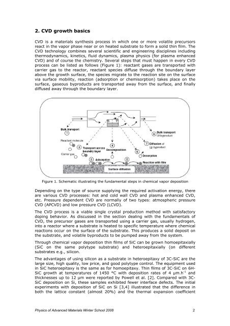
<strong>CVD</strong>) and of course the chemistry. Several steps that must happen in every <strong>CVD</strong><br />
process can be listed as follows (Figure 1): reactant gases are transported with<br />
carrier gas to the reactor, reactant species diffuse through the boundary layer<br />
above the <str<strong>on</strong>g>growth</str<strong>on</strong>g> surface, the species migrate to the reacti<strong>on</strong> site <strong>on</strong> the surface<br />
<strong>via</strong> surface mobility, reacti<strong>on</strong> (adsorpti<strong>on</strong> or chemisorpti<strong>on</strong>) takes place <strong>on</strong> the<br />
surface, gaseous byproducts are transported away from the surface, and finally<br />
diffused away through the boundary layer.<br />
Figure 1. Schematic illustrating the fundamental steps in chemical vapor depositi<strong>on</strong><br />
Depending <strong>on</strong> the type of source supplying the required activati<strong>on</strong> energy, there<br />
are various <strong>CVD</strong> processes: hot and cold wall <strong>CVD</strong> and plasma enhanced <strong>CVD</strong>,<br />
etc. Pressure dependent <strong>CVD</strong> are normally of two types: atmospheric pressure<br />
<strong>CVD</strong> (AP<strong>CVD</strong>) and low pressure <strong>CVD</strong> (L<strong>CVD</strong>).<br />
The <strong>CVD</strong> process is a <strong>via</strong>ble single crystal producti<strong>on</strong> method with satisfactory<br />
doping behavior. As discussed in the secti<strong>on</strong> dealing with the fundamentals of<br />
<strong>CVD</strong>, the precursor gases are transported using a carrier gas, usually hydrogen,<br />
into a reactor where a substrate is heated to specific temperature where chemical<br />
reacti<strong>on</strong>s occur <strong>on</strong> the surface of the substrate. This produces a solid deposit <strong>on</strong><br />
the substrate, and volatile byproducts to be pumped away from the system.<br />
Through chemical vapor depositi<strong>on</strong> thin films of <str<strong>on</strong>g><strong>Si</strong>C</str<strong>on</strong>g> can be grown homoepitaxially<br />
(<str<strong>on</strong>g><strong>Si</strong>C</str<strong>on</strong>g> <strong>on</strong> the same polytype substrate) and heteroepitaxially (<strong>on</strong> different<br />
<strong>substrates</strong> e.g., silic<strong>on</strong>.<br />
The advantages of using silic<strong>on</strong> as a substrate in heteroepitaxy of <str<strong>on</strong>g>3C</str<strong>on</strong>g>-<str<strong>on</strong>g><strong>Si</strong>C</str<strong>on</strong>g> are the<br />
large size, high quality, low price, and good polytype c<strong>on</strong>trol. The equipment used<br />
in <str<strong>on</strong>g><strong>Si</strong>C</str<strong>on</strong>g> heteroepitaxy is the same as for homoepitaxy. Thin films of <str<strong>on</strong>g>3C</str<strong>on</strong>g>-<str<strong>on</strong>g><strong>Si</strong>C</str<strong>on</strong>g> <strong>on</strong> 6H-<br />
<str<strong>on</strong>g><strong>Si</strong>C</str<strong>on</strong>g> <str<strong>on</strong>g>growth</str<strong>on</strong>g> at temperatures of 1450 °C with depositi<strong>on</strong> rates of 4 µm.h -1 and<br />
thicknesses up to 12 µm were reported by Powell et al. [2]. Compared with <str<strong>on</strong>g>3C</str<strong>on</strong>g>-<br />
<str<strong>on</strong>g><strong>Si</strong>C</str<strong>on</strong>g> depositi<strong>on</strong> <strong>on</strong> <strong>Si</strong>, these samples exhibited fewer interface defects. The initial<br />
experiments with depositi<strong>on</strong> of <str<strong>on</strong>g><strong>Si</strong>C</str<strong>on</strong>g> <strong>on</strong> <strong>Si</strong> [3,4] illustrated that the difference in<br />
both the lattice c<strong>on</strong>stant (almost 20%) and the thermal expansi<strong>on</strong> coefficient<br />
Physics of Advanced Materials Winter School 2008 2